


查询TPS2834供应商
TPS2834, TPS2835
SYNCHRONOUS-BUCK MOSFET DRIVERS
WITH DEADTIME CONTROL
SLVS223 – NOVEMBER 1999
D
Floating Bootstrap or Ground-Reference
High-Side Driver
D
Active Deadtime Control
D
50-ns Max Rise/Fall Times With 3.3-nF Load
D
2-A Min Peak Output Current
D
4.5-V to 15-V Supply Voltage Range
D
TTL-Compatible Inputs
D
Internal Schottky Bootstrap Diode
D
SYNC Control for Synchronous or
Nonsynchronous Operation
D
CROWBAR for OVP, Protects Against
ENABLE
CROWBAR
SYNC
PGND
NC – No internal connection
D OR PWP PACKAGE
1
IN
NC
DT
2
3
4
5
6
7
(TOP VIEW)
14
13
12
11
10
9
8
BOOT
NC
HIGHDR
BOOTLO
LOWDR
NC
V
CC
Faulted High-Side Power FETs
D
Low Supply Current ...3 mA Typ
D
Ideal for High-Current Single- or Multiphase
Applications
D
–40°C to 125°C Junction-Temperature
Operating Range
description
The TPS2834 and TPS2835 are MOSFET drivers for synchronous-buck power stages. These devices are ideal
for designing a high-performance power supply using a switching controller that does not include suitable
on-chip MOSFET drivers. The drivers are designed to deliver minimum 2-A peak currents into large capacitive
loads. The high-side driver can be configured as ground-reference or as floating-bootstrap. An adaptive
dead-time control circuit eliminates shoot-through currents through the main power FETs during switching
transitions, and provides high efficiency for the buck regulator. The TPS2834 and TPS2835 have additional
control functions: ENABLE, SYNC, and CROWBAR. Both high-side and low-side drivers are off when ENABLE
is low. The low-side driver is configured as a nonsynchronous-buck driver when SYNC is low . The CROWBAR
function turns on the low-side power FET, overriding the IN signal, for overvoltage protection against faulted
high-side power FETs.
The TPS2834 has a noninverting input, while the TPS2835 has an inverting input. These drivers are available
in 14-terminal SOIC and TSSOP packages and operate over a junction temperature range of –40°C to 125°C.
AVAILABLE OPTIONS
PACKAGED DEVICES
–40°C to 125°C
The D and PWP packages are available taped and reeled. Add R
suffix to device type (e.g., TPS2834DR)
Please be aware that an important notice concerning availability, standard warranty, and use in critical applications of
Texas Instruments semiconductor products and disclaimers thereto appears at the end of this data sheet.
PRODUCTION DATA information is current as of publication date.
Products conform to specifications per the terms of Texas Instruments
standard warranty. Production processing does not necessarily include
testing of all parameters.
T
J
POST OFFICE BOX 655303 • DALLAS, TEXAS 75265
SOIC
(D)
TPS2834D
TPS2835D
TSSOP
(PWP)
TPS2834PWP
TPS2835PWP
Copyright 1999, Texas Instruments Incorporated
1
TPS2834, TPS2835
I/O
DESCRIPTION
SYNCHRONOUS-BUCK MOSFET DRIVERS
WITH DEADTIME CONTROL
SLVS223 – NOVEMBER 1999
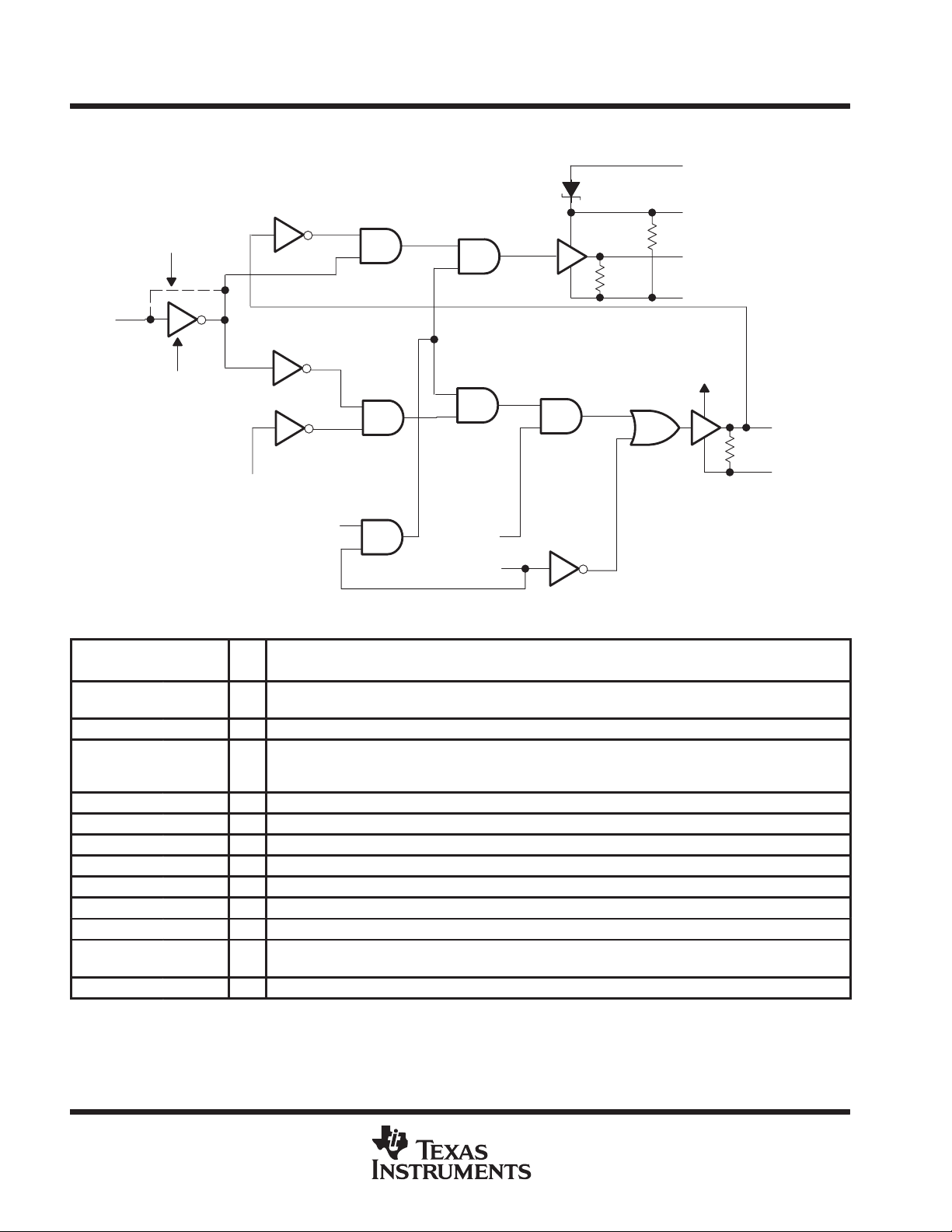
functional block diagram
(TPS2834 Only)
2
IN
(TPS2835 Only)
6
DT
200 kΩ
200 kΩ
8
14
12
11
V
CC
BOOT
HIGHDR
BOOTLO
V
CC
10
200 kΩ
7
LOWDR
PGND
ENABLE
1
SYNC
CROWBAR
5
3
Terminal Functions
TERMINAL
NAME NO.
BOOT 14 I Bootstrap terminal. A ceramic capacitor is connected between BOOT and BOOTLO to develop the floating
BOOTLO 11 O This terminal connects to the junction of the high-side and low-side MOSFETs.
CROWBAR 3 I CROWBAR can to be driven by an external OVP circuit to protect against a short across the high-side
DT 6 I Deadtime control terminal. Connect DT to the junction of the high-side and low-side MOSFETs.
ENABLE 1 I If ENABLE is low, both drivers are off.
HIGHDR 12 O Output drive for the high-side power MOSFET
IN 2 I Input signal to the MOSFET drivers (noninverting input for the TPS2834; inverting input for the TPS2835).
LOWDR 10 O Output drive for the low-side power MOSFET
NC 4, 9, 13
PGND 7 Power ground. Connect to the FET power ground
SYNC 5 I Synchronous rectifier enable terminal. If SYNC is low, the low-side driver is always off; If SYNC is high, the
V
CC
8 I Input supply. Recommended that a 1-µF capacitor be connected from VCC to PGND.
bootstrap voltage for the high-side MOSFET. The capacitor value is typically between 0.1 µF and 1 µF.
MOSFET. If CROWBAR is driven low, the low-side driver will be turned on and the high-side driver will be
turned off, independent of the status of all other control terminals.
low-side driver provides gate drive to the low-side MOSFET.
2
POST OFFICE BOX 655303 • DALLAS, TEXAS 75265

detailed description
low-side driver
TPS2834, TPS2835
SYNCHRONOUS-BUCK MOSFET DRIVERS
WITH DEADTIME CONTROL
SLVS223 – NOVEMBER 1999
The low-side driver is designed to drive low r
source and sink.
high-side driver
The high-side driver is designed to drive low r
source and sink. The high-side driver can be configured as a GND-reference driver or as a floating bootstrap
driver. The internal bootstrap diode is a Schottky, for improved drive ef ficiency. The maximum voltage that can
be applied from BOOT to ground is 30 V.
dead-time (DT) control
Dead-time control prevents shoot-through current from flowing through the main power FETs during switching
transitions by controlling the turnon times of the MOSFET drivers. The high-side driver is not allowed to turn
on until the gate drive voltage to the low-side FET is low, and the low-side driver is not allowed to turn on until
the voltage at the junction of the power FETs (Vdrn) is low; the TTL-compatible DT terminal connects to the
junction of the power FETs.
ENABLE
The ENABLE terminal enables the drivers. When enable is low, the output drivers are low. ENABLE is a
TTL-compatible digital terminal.
IN
The IN terminal is a TTL-compatible digital terminal that is the input control signal for the drivers. The TPS2834
has a noninverting input; the TPS2835 has an inverting input.
SYNC
N-channel MOSFET s. The current rating of the driver is 2 A,
DS(on)
N-channel MOSFET s. The current rating of the driver is 2 A,
DS(on)
The SYNC terminal controls whether the drivers operate in synchronous or nonsynchronous mode. In
synchronous mode, the low-side FET is operated as a synchronous rectifier. In nonsynchronous mode, the
low-side FET is always off. SYNC is a TTL-compatible digital terminal.
CROWBAR
The CROWBAR terminal overrides the normal operation of the driver. When CROWBAR is low, the low-side
FET turns on to act as a clamp, protecting the output voltage of the dc/dc converter against overvoltages due
to a short across the high-side FET. VIN should be fused to protect the low-side FET. CROWBAR is a
TTL-compatible digital terminal.
POST OFFICE BOX 655303 • DALLAS, TEXAS 75265
3
TPS2834, TPS2835
A
SYNCHRONOUS-BUCK MOSFET DRIVERS
WITH DEADTIME CONTROL
SLVS223 – NOVEMBER 1999
absolute maximum ratings over operating free-air temperature (unless otherwise noted)
Supply voltage range, V
(see Note 1) –0.3 V to 16 V. . . . . . . . . . . . . . . . . . . . . . . . . . . . . . . . . . . . . . . . . . . . .
CC
†
Input voltage range:BOOT to PGND (high-side driver ON) –0.3 V to 30 V. . . . . . . . . . . . . . . . . . . . . . . . . . . . .
BOOTLO to PGND –0.3 V to 16 V. . . . . . . . . . . . . . . . . . . . . . . . . . . . . . . . . . . . . . . . . . . . . .
BOOT to BOOTLO –0.3 V to 16 V. . . . . . . . . . . . . . . . . . . . . . . . . . . . . . . . . . . . . . . . . . . . . .
ENABLE, SYNC, and CROWBAR (see Note 2) –0.3 V to 16 V. . . . . . . . . . . . . . . . . . . . .
IN –0.3 V to 16 V. . . . . . . . . . . . . . . . . . . . . . . . . . . . . . . . . . . . . . . . . . . . . . . . . . . . . . . . . . . . .
DT –0.3 V to 30 V. . . . . . . . . . . . . . . . . . . . . . . . . . . . . . . . . . . . . . . . . . . . . . . . . . . . . . . . . . . .
Continuous total power dissipation See Dissipation Rating Table. . . . . . . . . . . . . . . . . . . . . . . . . . . . . . . . . . . . .
Operating virtual junction temperature range, T
Storage temperature range, T
–65°C to 150°C. . . . . . . . . . . . . . . . . . . . . . . . . . . . . . . . . . . . . . . . . . . . . . . . . . .
stg
–40°C to 125°C. . . . . . . . . . . . . . . . . . . . . . . . . . . . . . . . . . . . .
J
Lead temperature soldering 1,6 mm (1/16 inch) from case for 10 seconds 260°C. . . . . . . . . . . . . . . . . . . . . . .
†
Stresses beyond those listed under “absolute maximum ratings” may cause permanent damage to the device. These are stress ratings only, and
functional operation of the device at these or any other conditions beyond those indicated under “recommended operating conditions” is not
implied. Exposure to absolute-maximum-rated conditions for extended periods may affect device reliability.
NOTES: 1. Unless otherwise specified, all voltages are with respect to PGND.
DISSIPATION RATING TABLE
PACKAGE
D 760 mW 7.6 mW/°C 420 mW 305 mW
PWP 2400 mW 25 mW/°C 1275 mW 900 mW
TA ≤ 25°C
POWER RATING
DERATING FACTOR
ABOVE TA = 25°C
TA = 70°C
POWER RATING
TA = 85°C
POWER RATING
recommended operating conditions
MIN NOM MAX UNIT
Supply voltage, V
Input voltage BOOT to PGND 4.5 28 V
CC
4.5 15 V
electrical characteristics over recommended operating virtual junction temperature range,
= 6.5 V, ENABLE = High, CL = 3.3 nF (unless otherwise noted)
V
CC
supply current
PARAMETER TEST CONDITIONS MIN TYP MAX UNIT
V
CC
V
CC
NOTE 2: Ensured by design, not production tested.
Supply voltage range 4.5 15 V
Quiescent current
V
(ENABLE)
V
(ENABLE)
V
(ENABLE)
f
(SWX)
C
(HIGHDR)
See Note 2
= LOW, VCC =15 V 100
= HIGH, VCC =15 V 300 400
= HIGH,
= 200 kHz,
= 50 pF,
VCC =12 V,
BOOTLO grounded,
C
(LOWDR)
= 50 pF,
3 mA
µ
4
POST OFFICE BOX 655303 • DALLAS, TEXAS 75265
(see Note 2)
(see Note 2)
Duty cycle < 2%
(see Note 3)
Duty cycle < 2%
(see Note 3)
TPS2834, TPS2835
SYNCHRONOUS-BUCK MOSFET DRIVERS
WITH DEADTIME CONTROL
SLVS223 – NOVEMBER 1999
electrical characteristics over recommended operating virtual junction temperature range,
= 6.5 V, ENABLE = High, CL = 3.3 nF (unless otherwise noted) (continued)
V
CC
output drivers
PARAMETER TEST CONDITIONS MIN TYP MAX UNIT
High-side sink
(see Note 3)
Peak output current
Output resistance
NOTES: 2: Ensured by design, not production tested.
3. The pullup/pulldown circuits of the drivers are bipolar and MOSFET transistors in parallel. The peak output current rating is the
combined current from the bipolar and MOSFET transistors. The output resistance is the r
the voltage on the driver output is less than the saturation voltage of the bipolar transistor.
High-side source
(see Note 3)
Low-side sink
Low-side source
High-side sink (see Note 3)
High-side source (see Note 3)
Low-side sink (see Note 3)
Low-side source (see Note 3)
Duty cycle < 2%,
tpw < 100 µs
Duty cycle < 2%,
tpw < 100 µs
tpw < 100 µs
(see Note 2)
tpw < 100 µs
(see Note 2)
V
V
V
V
V
V
V
V
V
V
V
V
VCC = 4.5 V, V
,
VCC = 6.5 V, V
VCC = 12 V, V
VCC = 4.5 V, V
,
VCC = 6.5 V, V
VCC = 12 V, V
V
V
V
V
V
V
V
V
V
V
V
V
V
V
V
V
V
V
– V
(BOOT)
(HIGHDR)
– V
(BOOT)
(HIGHDR)
– V
(BOOT)
(HIGHDR)
– V
(BOOT)
(HIGHDR)
– V
(BOOT)
(HIGHDR)
– V
(BOOT)
(HIGHDR)
– V
(BOOT)
(HIGHDR)
– V
(BOOT)
(HIGHDR)
– V
(BOOT)
(HIGHDR)
– V
(BOOT)
(HIGHDR)
– V
(BOOT)
(HIGHDR)
– V
(BOOT)
(HIGHDR)
= 4.5 V, V
(DRV)
= 6.5 V, V
(DRV)
= 12 V, V
(DRV)
= 4.5 V, V
(DRV)
= 6.5 V, V
(DRV)
= 12 V, V
(DRV)
(BOOTLO)
= 4 V
(BOOTLO)
= 5 V
(BOOTLO)
= 10.5 V
(BOOTLO)
= 0.5V
(BOOTLO)
= 1.5 V
(BOOTLO)
= 1.5 V
(LOWDR)
(LOWDR)
(LOWDR)
LOWDR))
(LOWDR))
(LOWDR0)
(BOOTLO)
= 0.5 V
(BOOTLO)
= 0.5 V
(BOOTLO)
= 0.5 V
(BOOTLO)
= 4 V
(BOOTLO)
= 6 V
(BOOTLO)
=11.5 V
(LOWDR)
(LOWDR)
(LOWDR)
(LOWDR)
(LOWDR
(LOWDR)
= 4.5 V,
= 6.5 V,
= 12 V,
= 4.5 V,
= 6.5 V,
= 12 V,
= 4 V 1.3 1.8
= 5 V 2 2.5
= 10.5 V 3 3.5
= 0.5V 1.4 1.7
= 1.5 V 2 2.4
= 1.5 V 2.5 3
= 4.5 V,
= 6.5 V,
= 12 V,
= 4.5 V,
= 6.5 V,
= 12 V,
= 0.5 V 9
= 0.5 V 7.5
= 0.5 V 6
= 4 V 75
)= 6 V 75
= 11.5 V 75
0.7 1.1
1.1 1.5
2 2.4
1.2 1.4
1.3 1.6
2.3 2.7
of the MOSFET transistor when
DS(on)
5
5
5
75
75
75
A
A
A
A
Ω
Ω
Ω
Ω
POST OFFICE BOX 655303 • DALLAS, TEXAS 75265
5

TPS2834, TPS2835
LOWDR
Over the V
range (see Note 2)
V
DT
Over the V
range
Over the V
range
Rise time
Fall time
deadtime) (see Note 2)
Propagation delay time
deadtime) (see Note 2)
deadtime) (see Note 2)
HIGHDR (see Note 2)
SYNCHRONOUS-BUCK MOSFET DRIVERS
WITH DEADTIME CONTROL
SLVS223 – NOVEMBER 1999
electrical characteristics over recommended operating virtual junction temperature range,
= 6.5 V, ENABLE = High, CL = 3.3 nF (unless otherwise noted) (continued)
V
CC
deadtime control
PARAMETER TEST CONDITIONS MIN TYP MAX UNIT
High-level input voltage, V
Low-level input voltage, V
High-level input voltage, V
Low-level input voltage, V
NOTE 2: Ensured by design, not production tested.
IH
IL
IH
IL
CC
CC
digital control terminals (IN, CROWBAR, SYNC, ENABLE)
PARAMETER TEST CONDITIONS MIN TYP MAX UNIT
High-level input voltage, V
Low-level input voltage, V
IH
IL
CC
switching characteristics over recommended operating virtual junction temperature range,
ENABLE = High, C
p
Propagation delay time
Driver nonoverlap time
NOTE 2: Ensured by design, not production tested.
= 3.3 nF (unless otherwise noted)
L
PARAMETER TEST CONDITIONS MIN TYP MAX UNIT
HIGHDR output (see Note 2)
LOWDR output (see Note 2)
HIGHDR output (see Note 2)
LOWDR output (see Note 2)
HIGHDR going low (excluding
LOWDR going high (excluding
LOWDR going low (excluding
DT to LOWDR and LOWDR to
V
V
V
VCC = 4.5 V 40
VCC = 6.5 V 30
VCC = 12 V 30
V
V
V
VCC = 4.5 V 40
VCC = 6.5 V 30
VCC = 12 V 30
V
V
V
V
V
V
VCC = 4.5 V 80
VCC = 6.5 V 70
VCC = 12 V 60
VCC = 4.5 V 40 170
VCC = 6.5 V 25 135
VCC = 12 V 15 85
(BOOT)
(BOOT)
(BOOT)
(BOOT)
(BOOT)
(BOOT)
(BOOT)
(BOOT)
(BOOT)
(BOOT)
(BOOT)
(BOOT)
= 4.5 V, V
= 6.5 V, V
= 12 V, V
= 4.5 V, V
= 6.5 V, V
= 12 V, V
= 4.5 V, V
= 6.5 V, V
= 12 V, V
= 4.5 V, V
= 6.5 V, V
= 12 V, V
(BOOTLO)
(BOOTLO)
(BOOTLO)
(BOOTLO)
(BOOTLO)
(BOOTLO)
(BOOTLO)
(BOOTLO)
(BOOTLO)
(BOOTLO)
(BOOTLO)
(BOOTLO)
= 0 V 60
= 0 V 50
= 0 V 50
= 0 V 50
= 0 V 40
= 0 V 40
= 0 V 95
= 0 V 80
= 0 V 70
= 0 V 80
= 0 V 70
= 0 V 60
0.7V
CC
0.7V
CC
2 V
1
V
1 V
1 V
ns
ns
ns
ns
ns
ns
ns
ns
6
POST OFFICE BOX 655303 • DALLAS, TEXAS 75265

TPS2834, TPS2835
SYNCHRONOUS-BUCK MOSFET DRIVERS
WITH DEADTIME CONTROL
SLVS223 – NOVEMBER 1999
TYPICAL CHARACTERISTICS
50
45
40
35
30
– Rise Time – ns
25
r
t
20
15
10
50
45
RISE TIME
vs
SUPPLY VOLTAGE
CL = 3.3 nF
TJ = 25 °C
High Side
Low Side
5791112
46 810
VCC – Supply Voltage – V
Figure 1
RISE TIME
vs
JUNCTION TEMPERATURE
VCC = 6.5 V
CL = 3.3 nF
13
FALL TIME
vs
SUPPLY VOLTAGE
50
CL = 3.3 nF
45
40
35
30
– Fall Time – ns
f
25
t
20
15
1514
10
46 810
5791112
High Side
Low Side
VCC – Supply Voltage – V
TJ = 25 °C
13
1514
Figure 2
FALL TIME
vs
50
45
JUNCTION TEMPERATURE
VCC = 6.5 V
CL = 3.3 nF
40
35
30
25
– Rise Time – ns
r
t
20
15
10
High Side
Low Side
0 50 100
25 75–50 –25
TJ – Junction Temperature – °C
Figure 3
125
40
35
30
25
– Fall Time – ns
f
t
20
15
10
–50 –25
High Side
Low Side
25 75
0 50 100
TJ – Junction Temperature – °C
Figure 4
125
POST OFFICE BOX 655303 • DALLAS, TEXAS 75265
7

TPS2834, TPS2835
SYNCHRONOUS-BUCK MOSFET DRIVERS
WITH DEADTIME CONTROL
SLVS223 – NOVEMBER 1999
TYPICAL CHARACTERISTICS
150
140
130
120
110
100
90
80
70
60
50
40
– Low-to-High Propagation Delay Time – ns
30
PLH
t
20
150
140
130
120
110
100
90
80
70
60
50
40
– Low-to-High Propagation Delay Time – ns
30
PLH
t
20
LOW-TO-HIGH PROPAGATION DELAY TIME
vs
SUPPLY VOLTAGE, LOW TO HIGH LEVEL
CL = 3.3 nF
TJ = 25 °C
Low Side
5791112
46 810
VCC – Supply Voltage – V
13
Figure 5
LOW-TO-HIGH PROPAGATION DELAY TIME
vs
JUNCTION TEMPERATURE
VCC = 6.5 V
CL = 3.3 nF
High Side
Low Side
–25–50
TJ – Junction Temperature – °C
25 75
0 50 100
1514
125
HIGH-TO-LOW PROPAGATION DELAY TIME
vs
SUPPLY VOLTAGE, HIGH TO LOW LEVEL
150
140
130
120
110
100
90
80
70
60
50
40
– High-to-Low Propagation Delay Time – ns
30
PHL
t
20
46 810
5791112
VCC – Supply Voltage – V
High Side
Low Side
Figure 6
HIGH-TO-LOW PROPAGATION DELAY TIME
vs
150
140
130
120
110
100
90
80
70
60
50
40
– High-to-Low Propagation Delay Time – ns
30
PHL
t
20
JUNCTION TEMPERATURE
VCC = 6.5 V
CL = 3.3 nF
High Side
Low Side
–25–50
0 50 100
25 75
TJ – Junction Temperature – °C
CL = 3.3 nF
TJ = 25 °C
13
1514
125
Figure 7
8
POST OFFICE BOX 655303 • DALLAS, TEXAS 75265
Figure 8

TPS2834, TPS2835
SYNCHRONOUS-BUCK MOSFET DRIVERS
WITH DEADTIME CONTROL
SLVS223 – NOVEMBER 1999
TYPICAL CHARACTERISTICS
DRIVER-OUTPUT RISE TIME
vs
LOAD CAPACITANCE
1000
VCC = 6.5 V
TJ = 25 °C
100
High Side
– Rise Time – ns
r
10
t
1
0.01 1 10 100
0.1
CL – Load Capacitance – nF
Low Side
Figure 9
SUPPLY CURRENT
vs
SUPPLY VOLTAGE
500 kHz
300 kHz
200 kHz
100 kHz
50 kHz
25 kHz
12
VCC – Supply Voltage – V
I Supply Current – –Aµ
CC
6000
5500
5000
4500
4000
3500
3000
2500
2000
1500
1000
500
TJ = 25 °C
CL = 50 pF
0
46 810
14
16
DRIVER-OUTPUT FALL TIME
vs
LOAD CAPACITANCE
1000
VCC = 6.5 V
TJ = 25 °C
100
High Side
– Fall Time – ns
f
10
t
1
0.01 1 10 100
0.1
CL – Load Capacitance – nF
Low Side
Figure 10
SUPPLY CURRENT
vs
SUPPLY VOLTAGE
2 MHz
1 MHz
12
VCC – Supply Voltage – V
CC
I Supply Current – mA–
25
TJ = 25 °C
CL = 50 pF
20
15
10
5
0
46 810 14
16
Figure 11
POST OFFICE BOX 655303 • DALLAS, TEXAS 75265
Figure 12
9

TPS2834, TPS2835
SYNCHRONOUS-BUCK MOSFET DRIVERS
WITH DEADTIME CONTROL
SLVS223 – NOVEMBER 1999
TYPICAL CHARACTERISTICS
PEAK SOURCE CURRENT
vs
DRIVE VOLTAGE
4
TJ = 25 °C
3.5
3
2.5
2
1.5
1
Peak Source Current – A
0.5
0
46 810
Low Side
High Side
12
VCC – Supply Voltage – V
14
16
4
TJ = 25 °C
3.5
3
2.5
2
1.5
Peak Sink Current – A
1
0.5
0
46 810
Figure 13
INPUT THRESHOLD VOLTAGE
vs
2.00
TJ = 25 °C
SUPPLY VOLTAGE
2.00
VCC = 6.5 V
PEAK SINK CURRENT
vs
DRIVE VOLTAGE
Low Side
High Side
12
VCC – Supply Voltage – V
Figure 14
INPUT THRESHOLD VOLTAGE
vs
JUNCTION TEMPERATURE
14
16
1.80
1.60
1.40
– Input Threshold Voltage – V
1.20
IT
V
1.00
4.00 6.00 8.00 10.00 12.00 14.00 16.00
VCC – Supply Voltage – V
Figure 15
1.80
1.60
1.40
– Input Threshold Voltage – V
1.20
IT
V
1.00
–50.00 –25.00 0.00 25.00 50.00 75.00 100.00 125.00
TJ – Junction Temperature – °C
Figure 16
10
POST OFFICE BOX 655303 • DALLAS, TEXAS 75265

TPS2834, TPS2835
SYNCHRONOUS-BUCK MOSFET DRIVERS
WITH DEADTIME CONTROL
SLVS223 – NOVEMBER 1999
APPLICATION INFORMATION
Figure 17 shows the circuit schematic of a 100-kHz synchronous-buck converter implemented with a TL5001A
pulse-width-modulation (PWM) controller and a TPS2835 driver. The converter operates over an input range from
4.5 V to 12 V and has a 3.3-V output. The circuit can supply 3 A continuous load. The converter achieves an efficiency
of 94% for V
V
IN
IN
= 5 V, I
=1 A, and 93% for V
load
= 5 V, I
IN
load
= 3 A.
+
C10
100 µF
C5
100 µF
+
R1
1 kΩ
GND
C9
0.22 µF
1
ENABLE
2
IN
3
CROWBAR
4
NC
5
SYNC
6
DT
7
PGND
R8
121 kΩ
U1
TPS2835
BOOTLO
C14
1 µF
C1
1 µF
BOOT
NC
HIGHDR
LOWDR
NC
V
CC
C8
0.1 µF
1
OUT
6
DTC
5
SCP
V
CC
GND
14
13
12
11
10
9
8
2
COMP
8
U2
TL5001A
3
4
FB
7
RT
R9
90.9 kΩ
C15
1.0 µF
C2
0.033 µF
R6
1 MΩ
C3
0.0022 µF
R2
1.6 kΩ
R10
1.0 kΩ
R5
0 Ω
Q1
Si4410
R11
4.7 Ω
Q2
Si4410
C4
0.022 µFR3180 Ω
R4
2.32 kΩ
C11
0.47 µF
R7
3.3 Ω
C6
1000 pF
L1
27 µH
100 µF
C12
C7
100 µF
+
C13
10 µF
+
3.3 V
RTN
Figure 17. 3.3-V 3-A Synchronous-Buck Converter Circuit
POST OFFICE BOX 655303 • DALLAS, TEXAS 75265
11

TPS2834, TPS2835
SYNCHRONOUS-BUCK MOSFET DRIVERS
WITH DEADTIME CONTROL
SLVS223 – NOVEMBER 1999
APPLICATION INFORMATION
Great care should be taken when laying out the pc board. The power-processing section is the most critical and
will generate large amounts of EMI if not properly configured. The junction of Q1, Q2, and L1 should be very
tight. The connection from Q1 drain to the positive sides of C5, C10, and C1 1 and the connection from Q2 source
to the negative sides of C5, C10, and C11 should be as short as possible. The negative terminals of C7 and
C12 should also be connected to Q2 source.
Next, the traces from the MOSFET driver to the power switches should be considered. The BOOTLO signal from
the junction of Q1 and Q2 carries the large gate drive current pulses and should be as heavy as the gate drive
traces. The bypass capacitor (C14) should be tied directly across V
The next most sensitive node is the FB node on the controller (terminal 4 on the TL5001A). This node is very
sensitive to noise pick-up and should be isolated from the high-current power stage and be as short as possible.
The ground around the controller and low-level circuitry should be tied to the power ground as the output. If these
three areas are properly laid out, the rest of the circuit should not have other EMI problems and the power supply
will be relatively free of noise.
and PGND.
CC
12
POST OFFICE BOX 655303 • DALLAS, TEXAS 75265

TPS2834, TPS2835
SYNCHRONOUS-BUCK MOSFET DRIVERS
WITH DEADTIME CONTROL
SLVS223 – NOVEMBER 1999
MECHANICAL DATA
D (R-PDSO-G**) PLASTIC SMALL-OUTLINE PACKAGE
14 PIN SHOWN
0.050 (1,27)
14
1
0.069 (1,75) MAX
A
0.020 (0,51)
0.014 (0,35)
0.010 (0,25)
0.004 (0,10)
DIM
8
7
PINS **
0.010 (0,25)
0.157 (4,00)
0.150 (3,81)
M
0.244 (6,20)
0.228 (5,80)
Seating Plane
0.004 (0,10)
8
14
0.008 (0,20) NOM
0°–8°
16
Gage Plane
0.010 (0,25)
0.044 (1,12)
0.016 (0,40)
A MAX
A MIN
NOTES: A. All linear dimensions are in inches (millimeters).
B. This drawing is subject to change without notice.
C. Body dimensions do not include mold flash or protrusion, not to exceed 0.006 (0,15).
D. Falls within JEDEC MS-012
POST OFFICE BOX 655303 • DALLAS, TEXAS 75265
0.197
(5,00)
0.189
(4,80)
0.344
(8,75)
0.337
(8,55)
0.394
(10,00)
0.386
(9,80)
4040047/D 10/96
13

TPS2834, TPS2835
SYNCHRONOUS-BUCK MOSFET DRIVERS
WITH DEADTIME CONTROL
SLVS223 – NOVEMBER 1999
MECHANICAL DATA
PWP (R-PDSO-G**) PowerPAD PLASTIC SMALL-OUTLINE PACKAGE
20-PIN SHOWN
0,65
20
1
1,20 MAX
0,30
0,19
11
4,50
4,30
10
A
0,15
0,05
PINS **
DIM
M
0,10
6,60
6,20
Seating Plane
0,10
1614
Thermal Pad
(See Note D)
20
0,15 NOM
0°–8°
Gage Plane
0,25
0,75
0,50
2824
A MAX
A MIN
NOTES: A. All linear dimensions are in millimeters.
B. This drawing is subject to change without notice.
C. Body dimensions do not include mold flash or protrusions.
D. The package thermal performance may be enhanced by bonding the thermal pad to an external thermal plane. This pad is electrically
and thermally connected to the backside of the die and possibly selected leads.
E. Falls within JEDEC MO-153
PowerPAD is a trademark of Texas Instruments Incorporated.
5,10
4,90
5,10
4,90
6,60
6,40
7,90
7,70
9,80
9,60
4073225/E 03/97
14
POST OFFICE BOX 655303 • DALLAS, TEXAS 75265

IMPORTANT NOTICE
T exas Instruments and its subsidiaries (TI) reserve the right to make changes to their products or to discontinue
any product or service without notice, and advise customers to obtain the latest version of relevant information
to verify, before placing orders, that information being relied on is current and complete. All products are sold
subject to the terms and conditions of sale supplied at the time of order acknowledgement, including those
pertaining to warranty, patent infringement, and limitation of liability.
TI warrants performance of its semiconductor products to the specifications applicable at the time of sale in
accordance with TI’s standard warranty. Testing and other quality control techniques are utilized to the extent
TI deems necessary to support this warranty . Specific testing of all parameters of each device is not necessarily
performed, except those mandated by government requirements.
CERTAIN APPLICATIONS USING SEMICONDUCTOR PRODUCTS MAY INVOLVE POTENTIAL RISKS OF
DEATH, PERSONAL INJURY, OR SEVERE PROPERTY OR ENVIRONMENTAL DAMAGE (“CRITICAL
APPLICATIONS”). TI SEMICONDUCTOR PRODUCTS ARE NOT DESIGNED, AUTHORIZED, OR
WARRANTED TO BE SUITABLE FOR USE IN LIFE-SUPPORT DEVICES OR SYSTEMS OR OTHER
CRITICAL APPLICA TIONS. INCLUSION OF TI PRODUCTS IN SUCH APPLICATIONS IS UNDERST OOD TO
BE FULLY AT THE CUSTOMER’S RISK.
In order to minimize risks associated with the customer’s applications, adequate design and operating
safeguards must be provided by the customer to minimize inherent or procedural hazards.
TI assumes no liability for applications assistance or customer product design. TI does not warrant or represent
that any license, either express or implied, is granted under any patent right, copyright, mask work right, or other
intellectual property right of TI covering or relating to any combination, machine, or process in which such
semiconductor products or services might be or are used. TI’s publication of information regarding any third
party’s products or services does not constitute TI’s approval, warranty or endorsement thereof.
Copyright 1999, Texas Instruments Incorporated
 Loading...