Texas Instruments TPS2212IDBR, TPS2212IDB Datasheet
TPS2212
SINGLE-SLOT, PARALLEL INTERFACE POWER SWITCH
FOR LOW POWER PC CARD SLOTS
SLVS193 – APRIL 1999
1
POST OFFICE BOX 655303 • DALLAS, TEXAS 75265
D
Fully Integrated VCC and Vpp Switching for
Low Power Single-Slot PC Card Interface
D
Low r
DS(on)
(160-mΩ VCC Switches)
D
Low Current Limit, 450 mA (VCC) Typ
D
3.3-V Low-Voltage Mode
D
12-V Supply Can Be Disabled Except
During 12-V Flash Programming
D
Short-Circuit and Thermal Protection
D
Space-Saving 16-Pin SSOP (DB)
D
Compatible With 3.3-V, 5-V, and 12-V PC
Cards
D
Break-Before-Make Switching
D
Typical Applications Include: PCMCIA PC
Card Sockets in PDAs, PBXs, Bar Code
Scanners, Compact Flash and Smart Cards
description
The TPS2212 PC Card power-interface switch provides an integrated power-management solution for a single
low power PC Card. All of the discrete power MOSFET s, a logic section, current limiting, and thermal protection
for PC Card control are combined on a single integrated circuit, using the Texas Instruments LinBiCMOS
process. The circuit allows the distribution of 3.3-V , 5-V, and/or 12-V card power , and is compatible with many
PCMCIA controllers. The current-limiting feature eliminates the need for fuses, which reduces component count
and improves reliability. Current-limit reporting can help the user isolate a system fault to the PC Card.
The TPS2212 features a 3.3-V low-voltage mode that allows for 3.3-V switching without the need for 5 V . Bias
power can be derived from either the 3.3-V or 5-V inputs. This facilitates low-power system designs such as
sleep mode and pager mode, where only 3.3 V is available.
End equipment for the TPS2212 includes notebook computers, desktop computers, personal digital assistants
(PDAs), digital cameras, and bar-code scanners. This device is well suited for those applications which need to
limit the power provided to the PC card due to power supply constraints. In many applications, such as palm
computers, the system cannot allocate more than 200 mA of current to a PC card slot. For these lower power
applications, the TPS2212 provides the same advanced level of protection as the TPS221 1 provides for higher
power applications.
AVAILABLE OPTIONS
PACKAGED DEVICE
T
A
SMALL OUTLINE
(DB)
–40°C to 85°C TPS2212IDBLE
The DB package is only available left-end taped
and reeled (indicated by the LE suffix on the
device type, e.g. TPS2212IDBLE).
Copyright 1999, Texas Instruments Incorporated
PRODUCTION DATA information is current as of publication date.
Products conform to specifications per the terms of Texas Instruments
standard warranty. Production processing does not necessarily include
testing of all parameters.
Please be aware that an important notice concerning availability, standard warranty, and use in critical applications of
Texas Instruments semiconductor products and disclaimers thereto appears at the end of this data sheet.
PC Card is a trademark of PCMCIA (Personal Computer Memory Card International Association).
LinBiCMOS is a trademark of Texas Instruments Incorporated.
1
2
3
4
5
6
7
8
16
15
14
13
12
11
10
9
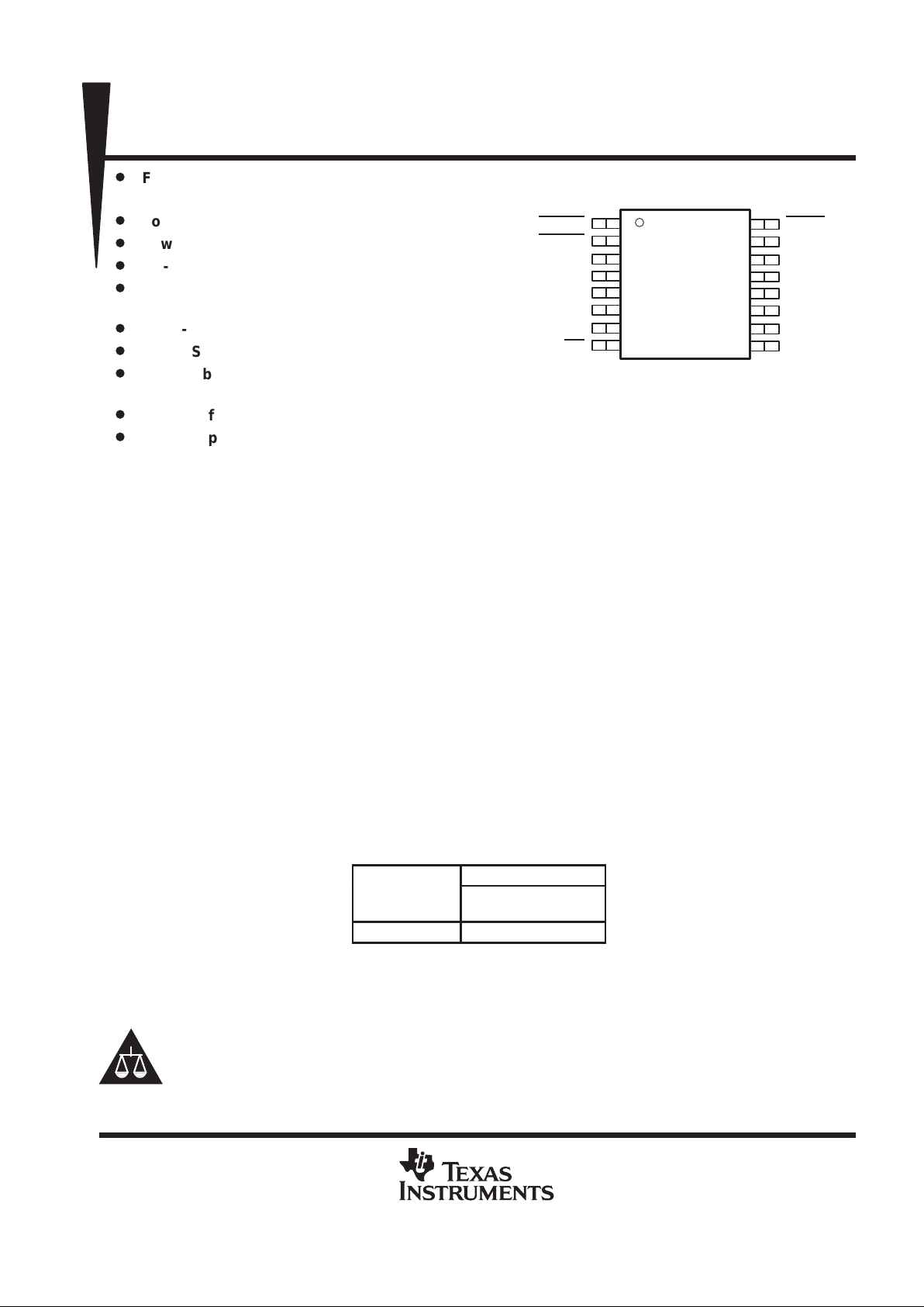
VCCD0
VCCD1
3.3V
3.3V
5V
5V
GND
OC
SHDN
VPPD0
VPPD1
VCC
VCC
VCC
VPP
VPPI
DB PACKAGE
(TOP VIEW)
TPS2212
SINGLE-SLOT, PARALLEL INTERFACE POWER SWITCH
FOR LOW POWER PC CARD SLOTS
SLVS193 – APRIL 1999
2
POST OFFICE BOX 655303 • DALLAS, TEXAS 75265
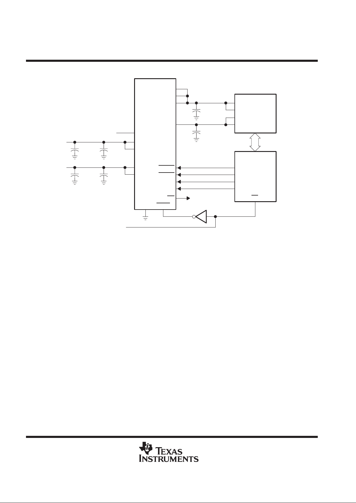
typical PC-card power-distribution application
VCC
VCC
VCC
VPP
VCCD0
VCCD1
VPPD0
VPPD1
OC
SHDNGND
0.1 µF
0.1 µF
V
CC1
V
CC2
V
pp1
V
pp2
PC Card
Connector
PCMCIA
Controller
VCC_EN0
VCC_EN1
VPP_EN0
VPP_EN1
CS
To CPU
TPS2212
VPPI
5V
5V
1 µF0.1 µF
5 V
3.3V
3.3V
1 µF0.1 µF
3.3 V
Shutdown Signal From CPU
3.3 V–12 V
TPS2212
SINGLE-SLOT, PARALLEL INTERFACE POWER SWITCH
FOR LOW POWER PC CARD SLOTS
SLVS193 – APRIL 1999
3
POST OFFICE BOX 655303 • DALLAS, TEXAS 75265
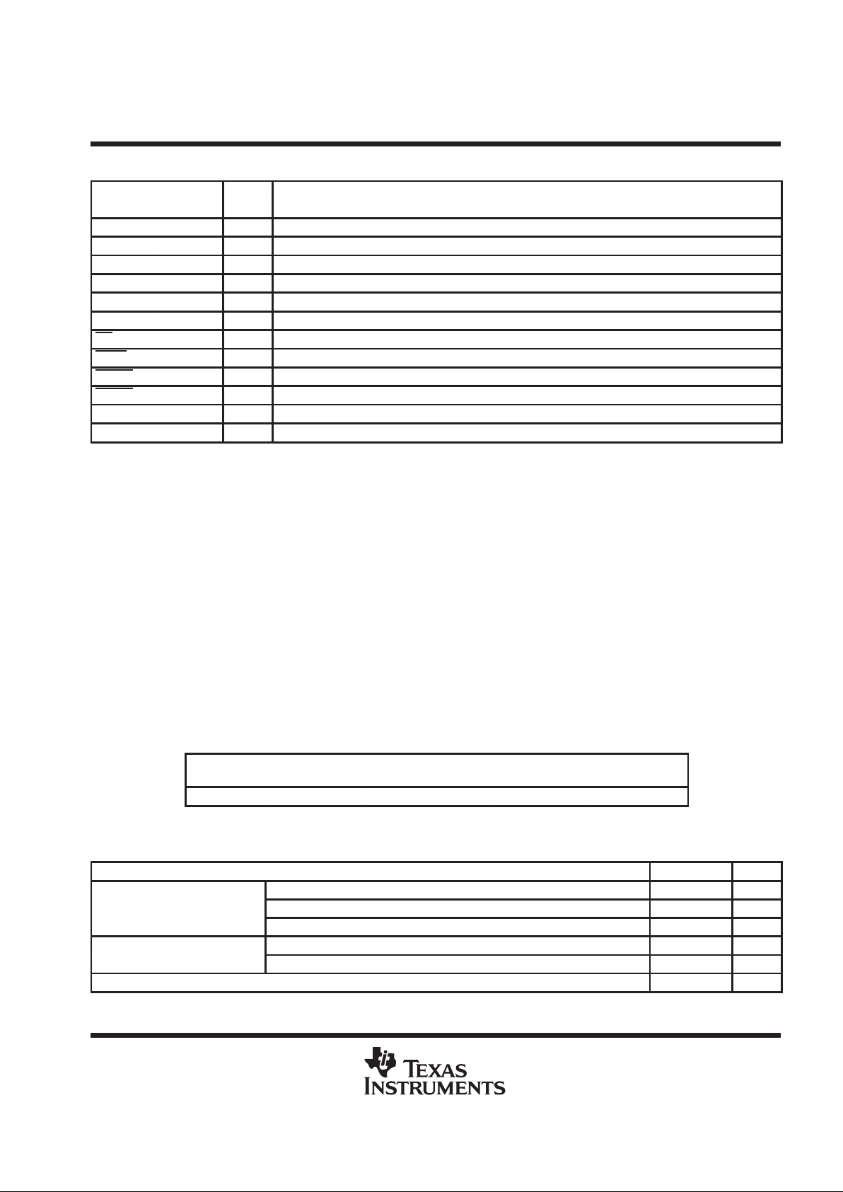
Terminal Functions
TERMINAL
NAME NO.
I/O
DESCRIPTION
3.3V 3, 4 I 3.3-V VCC input for card power and/or chip power if 5 V is not present
5V 5, 6 I 5-V VCC input for card power and/or chip power
VPPI 9 I Main VPP input, typically 12 V, allows 3.3 V–12 V.
VCC 11, 12, 13 O Switched output that delivers 0 V , 3.3-V, 5-V, or high impedance to card
VPP 10 O Switched output that delivers 0 V 3.3-V, 5-V, VPPI (12V), or high impedance to card
GND 7 Ground
OC 8 O Logic-level overcurrent reporting output that goes low when an overcurrent conditions exists
SHDN 16 I Logic input that shuts down the TPS2212 and sets all power outputs to high-impedance state
VCCD0 1 I Logic input that controls voltage of VCC (see control-logic table)
VCCD1 2 I Logic input that controls voltage of VCC (see control-logic table)
VPPD0 15 I Logic input that controls voltage of VPP (see control-logic table)
VPPD1 14 I Logic input that controls voltage of VPP (see control-logic table)
absolute maximum ratings over operating free-air temperature (unless otherwise noted)
†
Input voltage range for card power: V
I(5V)
–0.3 V to 7 V. . . . . . . . . . . . . . . . . . . . . . . . . . . . . . . . . . . . . . . . . . .
V
I(3.3V)
–0.3 V to 7 V. . . . . . . . . . . . . . . . . . . . . . . . . . . . . . . . . . . . . . . . .
V
I(VPPI)
–0.3 V to 14 V. . . . . . . . . . . . . . . . . . . . . . . . . . . . . . . . . . . . . . . .
Logic input voltage –0.3 V to 7 V. . . . . . . . . . . . . . . . . . . . . . . . . . . . . . . . . . . . . . . . . . . . . . . . . . . . . . . . . . . . . . . . .
Continuous total power dissipation See Dissipation Rating Table. . . . . . . . . . . . . . . . . . . . . . . . . . . . . . . . . . . . .
Output current (each card): I
O(VCC)
internally limited. . . . . . . . . . . . . . . . . . . . . . . . . . . . . . . . . . . . . . . . . . . . . .
I
O(VPP)
internally limited. . . . . . . . . . . . . . . . . . . . . . . . . . . . . . . . . . . . . . . . . . . . . .
Operating
virtual junction temperature range, T
J
–40°C to 150°C. . . . . . . . . . . . . . . . . . . . . . . . . . . . . . . . . . . . .
Operating free-air temperature range, T
A
–40°C to 85°C. . . . . . . . . . . . . . . . . . . . . . . . . . . . . . . . . . . . . . . . . . . .
Storage temperature range, T
stg
–55°C to 150°C. . . . . . . . . . . . . . . . . . . . . . . . . . . . . . . . . . . . . . . . . . . . . . . . . . .
Lead temperature 1.6 mm (1/16 inch) from case for 10 seconds 260°C. . . . . . . . . . . . . . . . . . . . . . . . . . . . . . .
†
Stresses beyond those listed under “absolute maximum ratings” may cause permanent damage to the device. These are stress ratings only, and
functional operation of the device at these or any other conditions beyond those indicated under “recommended operating conditions” is not
implied. Exposure to absolute-maximum-rated conditions for extended periods may affect device reliability.
DISSIPATION RATING TABLE
PACKAGE
TA ≤ 25°C
POWER RATING
DERATING FACTOR
ABOVE TA = 25°C
TA = 70°C
POWER RATING
TA = 85°C
POWER RATING
DB 775 mW 6.2 mW/°C 496 mW 403 mW
These devices are mounted on an FR4 board with no special thermal considerations.
recommended operating conditions
MIN MAX UNIT
V
I(5V)
0 5.25 V
Input voltage, V
I
V
I(3.3V)
0 5.25 V
V
I(VPPI)
0 13.5 V
p
I
O(VCC)
250 mA
Output Current
I
O(VPP)
150 mA
Operating virtual junction temperature, T
J
–40 125 °C
TPS2212
SINGLE-SLOT, PARALLEL INTERFACE POWER SWITCH
FOR LOW POWER PC CARD SLOTS
SLVS193 – APRIL 1999
4
POST OFFICE BOX 655303 • DALLAS, TEXAS 75265
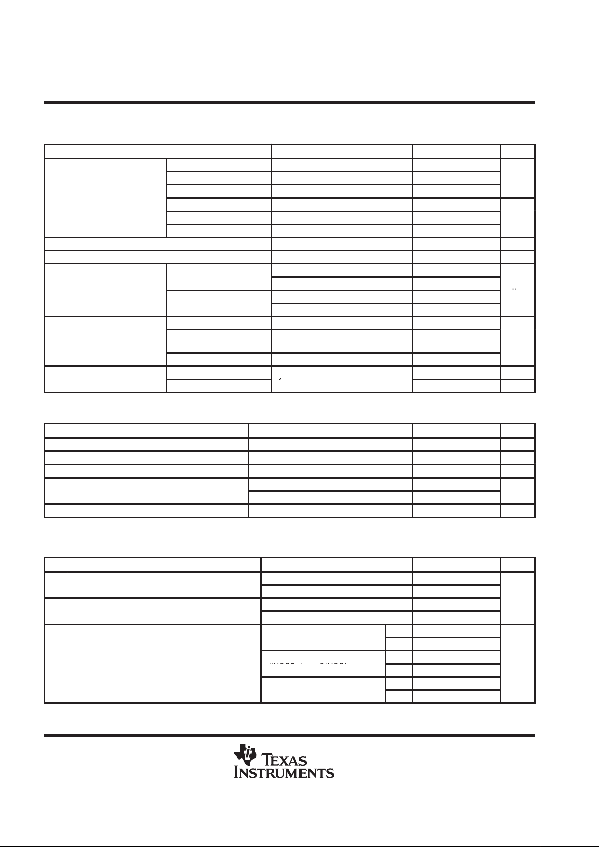
electrical characteristics, TA = –40°C to 85°C (unless otherwise noted)
power switch
PARAMETER
TEST CONDITIONS
†
MIN TYP MAX UNIT
5 V to VCC V
I(5V)
= 5 V 160 210
3.3 V to VCC V
I(5V)
= 5 V, V
I(3.3V)
= 3.3 V 160 210
mΩ
3.3 V to VCC V
I(5V)
= 0 V, V
I(3.3V)
= 3.3 V 160 210
Switch resistance
5 V to VPP TJ=25°C 6
3.3 V to VPP TJ=25°C 6
Ω
12 V to VPP TJ=25°C 1
V
O(VPP)
Clamp low voltage Ipp at 10 mA 0.8 V
V
O(VCC)
Clamp low voltage ICC at 10 mA 0.8 V
p
TA = 25°C 1 10
I
PP
high-impedance state
TA= 85°C 50
I
lkg
Leakage current
p
TA = 25°C 1 10
µ
A
I
CC
high-impedance state
TA=85°C 50
V
I(5V)
= 5 V V
O(VCC)
= 5 V, V
O(VPP)
= 12 V 40 150
I
I
Input current
V
I(5V)
= 0 V,
V
I(3.3V)
= 3.3 V
V
O(VCC)
= 3.3 V, V
O(VPP)
= 12 V 40 150
µA
Shutdown mode V
O(VCC)
= V
O(VPP)
= Hi-Z 1
Short-circuit
I
O(VCC)
TJ = 85°C, output powered into a
300 600 mA
I
OS
output-current limit
I
O(VPP)
J
short to GND
120 400 mA
†
Pulse-testing techniques maintain junction temperature close to ambient temperature; thermal effects must be taken into account separately.
logic section
PARAMETER
TEST CONDITIONS
†
MIN MAX UNIT
Logic input current 1 µA
Logic input high level 2 V
Logic input low level 0.8 V
p
V
I(5V)
= 5 V, IO = 1 mA V
I(5V)
– 0.4
Logic output high level
V
I(5V)
= 0 V, IO = 1 mA, V
I(3.3V)
= 3.3 V V
I(3.3V)
– 0.4
V
Logic output low level IO = 1 mA 0.4 V
†
Pulse-testing techniques maintain junction temperature close to ambient temperature; thermal effects must be taken into account separately.
switching characteristics
‡
PARAMETER
TEST CONDITIONS
§
MIN TYP MAX UNIT
p
V
O(VCC)
2.8
trRise times, output
V
O(VPP)
6.4
p
V
O(VCC)
4.5
ms
tfFall times, output
V
O(VPP)
12
t
on
6.8
V
I(VPPD0)
to
V
O(VPP)
t
off
18
p
t
on
4
tpdPropagation delay (see Figure1)
V
I(VCCD1)
to
V
O(VCC)
(3.
3V)
t
off
17
ms
t
on
6.6
V
I(VCCD0)
to
V
O(VCC)
(5V)
t
off
17
‡
Switching Characteristics are with CL = 150 µF.
§
Refer to Parameter Measurement Information
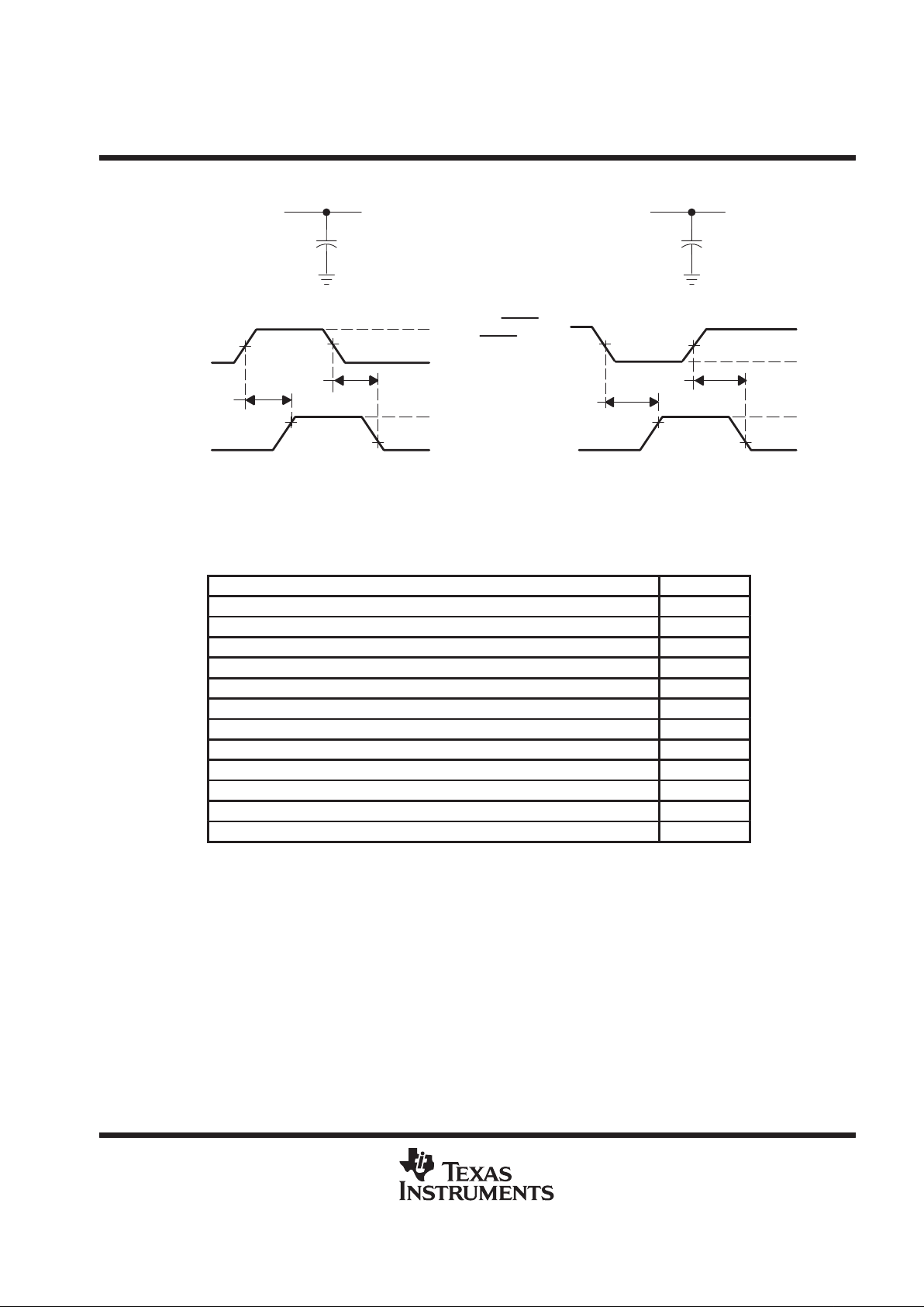
TPS2212
SINGLE-SLOT, PARALLEL INTERFACE POWER SWITCH
FOR LOW POWER PC CARD SLOTS
SLVS193 – APRIL 1999
5
POST OFFICE BOX 655303 • DALLAS, TEXAS 75265
PARAMETER MEASUREMENT INFORMATION
t
off
t
off
LOAD CIRCUIT
C
L
t
on
VOLTAGE WAVEFORMS
V
I(VPPI)
GND
50%
90%
V
DD
GND
(V
I(VPPD1)
= 0 V)
V
O(VPP)
AVPP
LOAD CIRCUIT
C
L
AVCC
VOLTAGE WAVEFORMS
V
I(3.3V)
GND
50%
90%
10%
V
DD
GND
(V
I(VCCD0)
= VDD)
V
O(VCC)
10%
t
on
50%
50%
V
I(VPPD0)
V
I(VCCD1)
Figure 1. Test Circuits and Voltage Waveforms
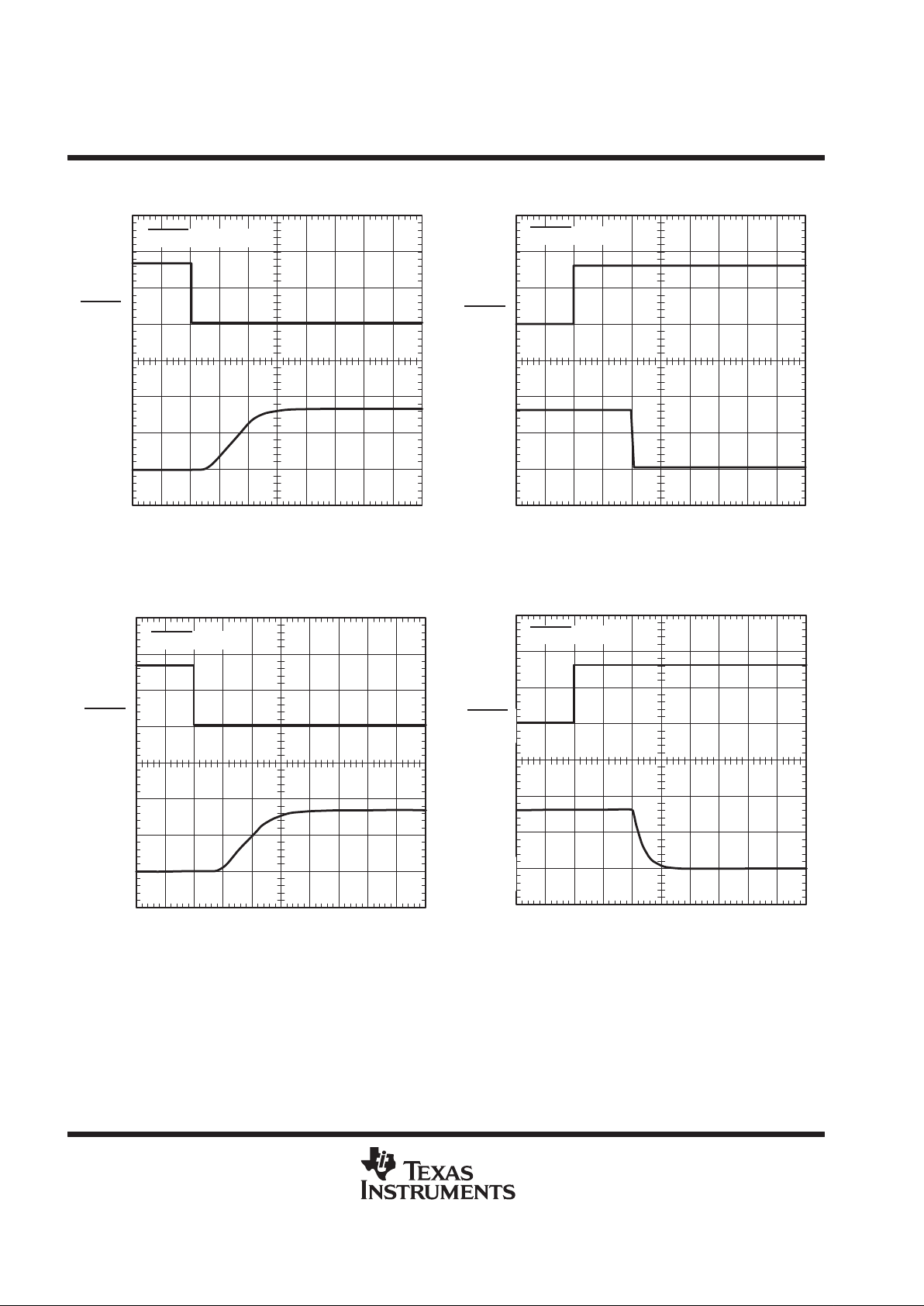
Table of Timing Diagrams
FIGURE
VCC Propagation Delay and Rise Time With 1-µF Load, 3.3-V Switch 2
VCC Propagation Delay and Fall Time With 1-µF Load, 3.3-V Switch 3
VCC Propagation Delay and Rise Time With 150-µF Load, 3.3-V Switch 4
VCC Propagation Delay and Fall Time With 150-µF Load, 3.3-V Switch 5
VCC Propagation Delay and Rise Time With 1-µF Load, 5-V Switch 6
VCC Propagation Delay and Fall Time With 1-µF Load, 5-V Switch 7
VCC Propagation Delay and Rise Time With 150-µF Load, 5-V Switch 8
VCC Propagation Delay and Fall Time With 150-µF Load, 5-V Switch 9
VPP Propagation Delay and Rise Time With 1-µF Load, 12-V Switch 10
VPP Propagation Delay and Fall Time With 1-µF Load, 12-V Switch 11
VPP Propagation Delay and Rise Time With 150-µF Load, 12-V Switch 12
VPP Propagation Delay and Fall Time With 150-µF Load, 12-V Switch 13
TPS2212
SINGLE-SLOT, PARALLEL INTERFACE POWER SWITCH
FOR LOW POWER PC CARD SLOTS
SLVS193 – APRIL 1999
6
POST OFFICE BOX 655303 • DALLAS, TEXAS 75265
PARAMETER MEASUREMENT INFORMATION
Figure 2. VCC Propagation Delay and Rise Time
With 1-µF Load, 3.3-V Switch
032145768910
VCCD0 = 3.3 V
t – Time – ms
VCCD1
(2 V/div)
VCC
(2 V/div)
Figure 3. VCC Propagation Delay and Fall Time
With 1-µF Load, 3.3-V Switch
01510520253530 40 45 50
VCCD0 = 3.3 V
t – Time – ms
VCCD1
(2 V/div)
VCC
(2 V/div)
Figure 4. VCC Propagation Delay and Rise Time
With 150-µF Load, 3.3-V Switch
032145768910
VCCD0 = 3.3 V
t – Time – ms
VCCD1
(2 V/div)
VCC
(2 V/div)
Figure 5. VCC Propagation Delay and Fall Time
With 150-µF Load, 3.3-V Switch
01510520253530 40 45 50
VCCD0 = 3.3 V
t – Time – ms
VCCD1
(2 V/div)
VCC
(2 V/div)
 Loading...