Texas Instruments TPS2120, TPS2121 Datasheet
www.ti.com
TPS2120, TPS2121
SLVSEA3F – AUGUST 2018 – REVISED AUGUST 2020
SLVSEA3F – AUGUST 2018 – REVISED AUGUST 2020
TPS2120, TPS2121
TPS212x 2.8-V to 22-V Priority Power MUX with Seamless Switchover
1 Features
• Wide operating range: 2.8 V to 22 V
– Absolute maximum input voltage of 24 V
• Low RON resistance:
– TPS2120: 62 mΩ (typical)
– TPS2121: 56 mΩ (typical)
• Adjustable overvoltage supervisor (OVx):
– Accuracy < ±5%
• Adjustable priority supervisor (PR1):
– Accuracy < ±5%
• TPS2121 Supports external voltage reference
(CP2) with an accuracy of <1%
• Output current limit (ILM):
– TPS2120: 1 A – 3 A
– TPS2121: 1 A – 4.5 A
• Channel status indication (ST)
• Adjustable input settling time (SS)
• Adjustable output soft start time (SS)
• TPS2121 Fast output switchover (tSW): 5 µs
(typical)
• Low Iq from enabled input: 200 µA (typical)
• Low Iq from disabled input: 10 µA (Typical)
• Manual input source selection (OVx)
• Over temperature protection (OTP)
2 Applications
• Backup and standby power
• Input source selection
• Multiple battery management
• EPOS and barcode scanners
• Building automation and surveillance
• Tracking and telematics
3 Description
The TPS212x devices are Dual-Input, Single-Output
(DISO) Power Multiplexer (MUX) that are well suited
for a variety of systems having multiple power
sources. The devices will Automatically Detect,
Select, and Seamlessly Transition between available
inputs.
Priority can be automatically given to the highest
input voltage or manually assigned to a lower voltage
input to support both ORing and Source Selection
operations. A priority voltage supervisor is used to
select an input source.
An Ideal Diode operation is used to seamlessly
transition between input sources. During switchover,
the voltage drop is controlled to block reverse current
before it happens and provide uninterrupted power to
the load with minimal hold-up capacitance.
Current limiting is used during startup and switchover
to protect against overcurrent events, and also
protects the device during normal operation. The
output current limit can be adjusted with a single
external resistor.
The TPS212x devices are available in WCSP and
small VQFN-HR package options characterized for
operation for a temperature range of –40°C to 125°C.
Device Information
PART NUMBER PACKAGE
TPS2120 WCSP (20) 1.5 mm x 2.0 mm
TPS2121 VQFN-HR (12) 2.0 mm x 2.5 mm
(1) For all available packages, see the orderable addendum at
the end of the data sheet.
(1)
BODY SIZE (NOM)
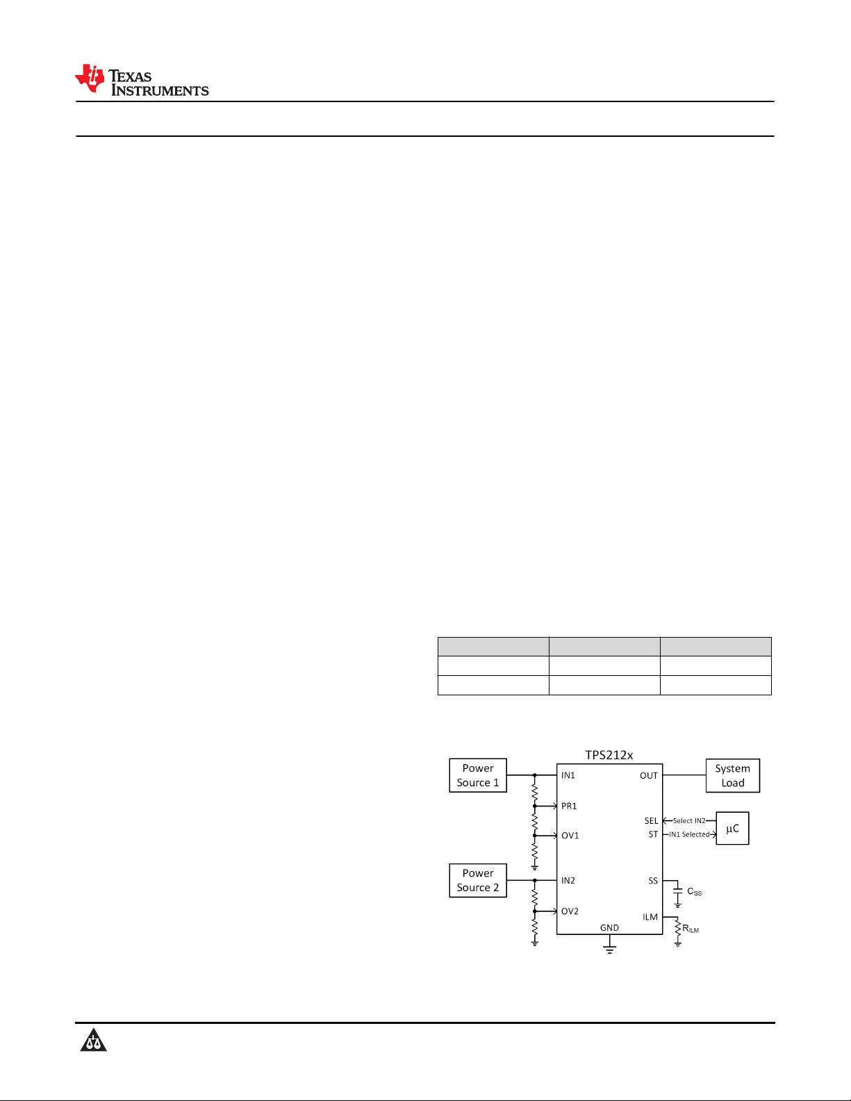
Typical Application
An IMPORTANT NOTICE at the end of this data sheet addresses availability, warranty, changes, use in safety-critical applications,
Copyright © 2020 Texas Instruments Incorporated
intellectual property matters and other important disclaimers. PRODUCTION DATA.
Product Folder Links: TPS2120 TPS2121
Submit Document Feedback
1

TPS2120, TPS2121
SLVSEA3F – AUGUST 2018 – REVISED AUGUST 2020
www.ti.com
Table of Contents
1 Features............................................................................1
2 Applications..................................................................... 1
3 Description.......................................................................1
4 Revision History.............................................................. 2
5 Device Comparison Table...............................................3
6 Pin Configuration and Functions...................................4
7 Specifications.................................................................. 6
7.1 Absolute Maximum Ratings........................................ 6
7.2 ESD Ratings............................................................... 6
7.3 Recommended Operating Conditions.........................6
7.4 Thermal Information....................................................6
7.5 Electrical Characteristics.............................................7
7.6 Typical Characteristics................................................9
8 Parameter Measurement Information.......................... 10
9 Detailed Description...................................................... 11
9.1 Overview................................................................... 11
9.2 Functional Block Diagram......................................... 11
9.3 Feature Description...................................................12
9.4 TPS2120 Device Functional Modes..........................18
9.5 TPS2121 Device Functional Modes..........................18
10 Application and Implementation................................ 19
10.1 Application Information........................................... 19
10.2 Typical Application.................................................. 19
10.3 Automatic Switchover with Priority (XCOMP)......... 25
10.4 Automatic Seamless Switchover with Priority
(XREF)........................................................................ 27
10.5 Highest Voltage Operation (VCOMP)..................... 28
10.6 Reverse Polarity Protection with TPS212x............. 31
10.7 Hotplugging with TPS212x......................................31
11 Power Supply Recommendations..............................33
12 Layout...........................................................................33
12.1 Layout Guidelines................................................... 33
12.2 Layout Example...................................................... 33
13 Device and Documentation Support..........................34
13.1 Documentation Support.......................................... 34
13.2 Receiving Notification of Documentation Updates..34
13.3 Support Resources................................................. 34
13.4 Trademarks.............................................................34
13.5 Electrostatic Discharge Caution..............................34
13.6 Glossary..................................................................34
14 Mechanical, Packaging, and Orderable
Information.................................................................... 34
4 Revision History
NOTE: Page numbers for previous revisions may differ from page numbers in the current version.
Changes from Revision E (February 2020) to Revision F (August 2020) Page
• Updated the numbering format for tables, figures and cross-references throughout the document ..................1
Changes from Revision D (September 2019) to Revision E (February 2020) Page
• Updated the Leakage Current in the Electrical Characteristics table in the Specifications section.................... 6
Changes from Revision C (February 2019) to Revision D (September 2019) Page
• Updated the Reverse Polarity Protection with TPS212x section ..................................................................... 31
• Updated the Hotplugging with TPS212x section ............................................................................................. 31
Changes from Revision B (December 2018) to Revision C (February 2019) Page
• Changed the Adjustable Overvoltage Supervisor (OVx) Accuracy to < ±5% in the Features section................ 1
• Changes made in the Recommended Operating Conditions and Electrical Characteristics table in the
Specifications section......................................................................................................................................... 6
• Changes made in the Active Current Limiting (ILM) section.............................................................................13
• Changed (typical) from 170°C to 160°C in the Thermal Protection (TSD) section............................................ 14
• Changed Equation 8 and Equation 9 ...............................................................................................................23
Changes from Revision A (November 2018) to Revision B (December 2018) Page
• Changed from Advance Information to Production Data.................................................................................... 1
Changes from Revision * (August 2018) to Revision A (November 2018) Page
• Changed Wide Operating Range to 2.7 V to 22 V..............................................................................................1
• Revised the Application and Implementation section....................................................................................... 19
2 Submit Document Feedback
Copyright © 2020 Texas Instruments Incorporated
Product Folder Links: TPS2120 TPS2121

www.ti.com
SLVSEA3F – AUGUST 2018 – REVISED AUGUST 2020
5 Device Comparison Table
Part Number Package On-Resistance Maximum Current Fastest Switchover Unique Pin
TPS2120 WCSP (20) 62 mΩ 3 A 100 us SEL
TPS2121 VQFN-HR (12) 56 mΩ 4.5 A 5 us CP2
TPS2120, TPS2121
Copyright © 2020 Texas Instruments Incorporated
Product Folder Links: TPS2120 TPS2121
Submit Document Feedback
3
TPS2120, TPS2121
SLVSEA3F – AUGUST 2018 – REVISED AUGUST 2020
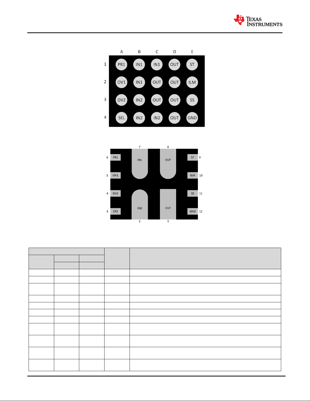
6 Pin Configuration and Functions
Figure 6-1. TPS2120 (YFP) Package 20-Pin WCSP Bottom View
www.ti.com
Figure 6-2. TPS2121 (RUX) Package 12-Pin VQFN-HR Bottom View
Pin Functions
PIN
NAME
IN1 B1, B2, C1 7 I Power Input for Source 1
IN2 B3, B4, C4 2 I Power Input for Source 2
OUT
ST E1 9 O Status output indicating which channel is selected. Connect to GND if not required.
ILIM E2 10 O Output Current Limiting for both channels.
SS E3 11 O Adjusts Input Setting Delay Time and Output Soft Start Time
GND E4 12 — Device Ground
PR1 A1
OV1 A2
OV2 A3
SEL A4
TPS2120 TPS2121
WCSP VQFN-HR
C2, C3, D1,
D2, D3, D4
1, 8
6
5
4
—
I/O DESCRIPTION
I Power Output
Enables Priority Operation. Connect to IN1 to set switchover voltage. Connect to
I
GND if not required.
Active Low Enable Supervisor for IN1 Overvoltage Protection. Connect to GND if
I
not required.
Active Low Enable Supervisor for IN2 Overvoltage Protection. Connect to GND if
I
not required.
Active low Enable for IN1. Allows GPIO to override priority operation and manually
I
select IN2. TPS2120 only.
4 Submit Document Feedback
Copyright © 2020 Texas Instruments Incorporated
Product Folder Links: TPS2120 TPS2121

www.ti.com
NAME
CP2 —
TPS2120 TPS2121
PIN
WCSP VQFN-HR
3
SLVSEA3F – AUGUST 2018 – REVISED AUGUST 2020
Pin Functions (continued)
I/O DESCRIPTION
Enables Comparator Operation and is compared to PR1 to set switchover voltage.
I
Connect to GND if not required. TPS2121 only.
TPS2120, TPS2121
Copyright © 2020 Texas Instruments Incorporated
Product Folder Links: TPS2120 TPS2121
Submit Document Feedback
5

TPS2120, TPS2121
SLVSEA3F – AUGUST 2018 – REVISED AUGUST 2020
www.ti.com
7 Specifications
7.1 Absolute Maximum Ratings
over operating free-air temperature range (unless otherwise noted)
V
, V
,
, V
,
IN2
Maximum Power Pin Voltage
Maximum Overvoltage Pin Voltage OV1, OV2 -0.3 6 V
Maximum Control Pin Voltage PRI, SEL -0.3 6 V
SEL
Maximum Control Pin Voltage ST -0.3 6 V
Maximum Output Current OUT Internally Limited
Maximum Junction Temperature Internally Limited
Storage temperature -65 150 °C
IN1
V
OUT
V
OV1
V
OV2
V
PRI
V
ST
I
OUT
T
J, MAX
T
STG
(1) Stresses beyond those listed under Absolute Maximum Rating may cause permanent damage to the device. These are stress ratings
only, which do not imply functional operation of the device at these or any other conditions beyond those indicated under
Recommended Operating Condition. Exposure to absolute-maximum-rated conditions for extended periods may affect device
reliability.
7.2 ESD Ratings
Human body model (HBM), per ANSI/ESDA/
V
ESD
Electrostatic discharge
JEDEC JS-001,
Charged device model (CDM), per JEDEC
specification JESD22-C101,
(1)
(1)
Pins MIN MAX UNIT
IN1, IN2,
OUT
-0.3 24 V
Pins VALUE UNIT
All ±2000
(2)
All ±500
V
(1) JEDEC document JEP155 states that 500-V HBM allows safe manufacturing with a standard ESD control process.
(2) JEDEC document JEP157 states that 250-V CDM allows safe manufacturing with a standard ESD control process.
7.3 Recommended Operating Conditions
over operating free-air temperature range (unless otherwise noted)
Pins MIN MAX UNIT
V
, V
IN1
V
OUT
V
OV1
V
OV2
V
, V
PRI
V
ST
R
ST
R
ILM
V
SS
I
, I
IN1
I
, I
IN1
T
J
Input Voltage Range
IN2
Output Voltage Range OUT 0 22 V
,
Overvoltage Pin Voltage OV1, OV2 0 5.5 V
Control Pin Voltage PRI, SEL 0 5.5 V
SEL
Control Pin Voltage ST 0 5.5 V
Status Pin Pull Up Resistance ST 6 20 kΩ
Current Limit Resistance ILM 18 100 kΩ
SS Pin Output Voltage SS 4 V
TPS2120 Continuous Input Current IN1, IN2 3 A
IN2
TPS2121 Continuous Input Current IN1, IN2 4.5 A
IN2
Junction temperature - -40 125 °C
(1) See Power Supply Recommendations Section for more Details
7.4 Thermal Information
THERMAL METRIC
R
θJA
Junction-to-ambient thermal resistance 72.5 72.2 °C/W
(1)
IN1, IN2 2.8 22 V
TPS2120 TPS2121
(1)
20 PINS 11 PINS
UNITYFP (WCSP) RNW (PKG FAM)
6 Submit Document Feedback
Copyright © 2020 Texas Instruments Incorporated
Product Folder Links: TPS2120 TPS2121

www.ti.com
SLVSEA3F – AUGUST 2018 – REVISED AUGUST 2020
7.4 Thermal Information (continued)
TPS2120, TPS2121
TPS2120 TPS2121
THERMAL METRIC
(1)
UNITYFP (WCSP) RNW (PKG FAM)
20 PINS 11 PINS
R
θJC(top)
R
θJB
Ψ
JT
Ψ
JB
R
θJC(bot)
Junction-to-case (top) thermal resistance 0.5 38.5 °C/W
Junction-to-board thermal resistance 16.4 15.4 °C/W
Junction-to-top characterization parameter 0.3 0.9 °C/W
Junction-to-board characterization parameter 16.6 15.5 °C/W
Junction-to-case (bottom) thermal resistance N/A N/A °C/W
(1) For more information about traditional and new thermal metrics, see the Semiconductor and IC Package Thermal Metrics application
report.
7.5 Electrical Characteristics
over operating free-air temperature range (unless otherwise noted)
PARAMETER TEST CONDITIONS T
INPUT SOURCE (IN1, IN2)
I
Q, INx
I
SBY, INx
I
LK, INx
V
Quiescent Current
(INx Powering OUT)
Standby Current
(INx not powering OUT)
Leakage Current
(INx to OUT)
Undervoltage Lockout
UV, INx
OUTPUT SWITCHOVER (OUT)
t
SW
t
FSW
V
Switchover Time
Fast Switchover Time
(TPS2121 only)
Input Voltage Comparator
COMP
(V
referenced to V
IN2
ON-RESISTANCE (INx to OUT)
ON-State Resistance (TPS2120)
R
ON
ON-State Resistance (TPS2121)
CURRENT LIMIT (ILM)
(1)
IN1
J
OUT = Open -40°C to 125°C 300 400 µA
V
= V
INx
(1)
OUT
25°C 0 15 25 µA
-40°C to 125°C 25 µA
25°C -1 1 µA
|V
- V
INx
OUT
| ≤ 5V
-40°C to 85°C -5 5 µA
-40°C to 125°C -80 80 µA
25°C -1 1 µA
|V
- V
INx
OUT
| ≤ 22V
-40°C to 85°C -35 35 µA
-40°C to 125°C -500 500 µA
V
Rising -40°C to 125°C 2.5 2.65 2.8 V
INx
V
Falling -40°C to 125°C 2.4 2.55 2.7 V
INx
V
< V
OUT
OUT
IN1
IN1
INx
REF
< V
INx
REF
≥ V
IN2
> V
, Falling Hysteresis -40°C to 125°C 2.5 3.5 4.5 %
IN2
CP2 or SEL < V
V
CP2 ≥ V
V
)
V
-40°C to 125°C 100 µs
-40°C to 125°C 5 µs
-40°C to 125°C 0 280 600 mV
25°C 62 75 mΩ
I
= -200 mA
OUT
V
V
PRI
INx
> V
REF
≥ 5.0 V
-40°C to 85°C 90 mΩ
-40°C to 105°C 100 mΩ
-40°C to 125°C 120 mΩ
25°C 56 70 mΩ
I
= -200 mA
OUT
V
V
PRI
INx
> V
REF
≥ 5.0 V
-40°C to 85°C 85 mΩ
-40°C to 105°C 90 mΩ
-40°C to 125°C 100 mΩ
MIN TYP MAX UNIT
Copyright © 2020 Texas Instruments Incorporated
Product Folder Links: TPS2120 TPS2121
Submit Document Feedback
7

TPS2120, TPS2121
SLVSEA3F – AUGUST 2018 – REVISED AUGUST 2020
7.5 Electrical Characteristics (continued)
over operating free-air temperature range (unless otherwise noted)
PARAMETER TEST CONDITIONS T
R
= 31.6kΩ -40°C to 125°C 3 3.5 4 A
ILM
R
= 46.4kΩ -40°C to 125°C 2 2.5 3 A
Output Current Limit (TPS2120)
(2)
I
LM
Output Current Limit (TPS2121)
(3)
t
LM
Current Limit Response Time Output Steady State -40°C to 125°C 250 µs
CONTROL PINS (PRI, SEL, OV1, OV2)
V
V
I
LK, x
Internal Voltage Reference
REF, x
Comparator Offset Voltage
OFST
(TPS2121 only)
Pin Leakage Current
STATUS INDICATION PIN (ST)
I
LK, ST
t
ST
Pin Leakage VST = 0 V to 5.5 V -40°C to 125°C -0.1 0.1 µA
Status Delay L to H -40°C to 125°C 1 µs
FAST REVERSE CURRENT BLOCKING (RCB)
I
RCB
V
t
RCB
Fast Reverse Current Detection
Threshold
RCB Release Voltage V
RCB
Fast Reverse Current Blocking
Response Time
THERMAL SHUTDOWN (TSD)
T
Thermal Shutdown
SD
ILM
R
= 85kΩ -40°C to 125°C 1 1.5 2 A
ILM
R
< 1kΩ -40°C to 125°C 1.5 2.5 3.5 A
ILM
R
= 18.7kΩ -40°C to 125°C 4.6 5.2 5.8 A
ILM
R
= 22.1kΩ -40°C to 125°C 4 4.5 5 A
ILM
R
= 29.8kΩ -40°C to 125°C 3 3.5 4 A
ILM
R
= 44.2kΩ -40°C to 125°C 2 2.5 3 A
ILM
R
= 80kΩ -40°C to 125°C 1 1.5 2 A
ILM
R
< 1kΩ -40°C to 125°C 1.5 2.5 3.5 A
ILM
V
, V
PR1
CP2, VOV1
V
, V
PR1
CP2, VOV1
V
> V
PR1
V
> V
CP2
V
, V
PR1
CP2, VOV1
REF
REF
, V
Rising -40°C to 125°C 1.01 1.06 1.1 V
OV2
, V
Falling -40°C to 125°C 0.99 1.04 1.09 V
OV2
, V
= 0 V to 5.5
OV2
V
V
> V
OUT
INx
> V
OUT
INx
Shutdown Rising 160 °C
Recovery Falling 150 °C
www.ti.com
J
MIN TYP MAX UNIT
-40°C to 125°C 5 20 40 mV
-40°C to 125°C -0.1 0.1 µA
-40°C to 125°C 0.2 1 2 A
-40°C to 125°C 0 25 50 mV
-40°C to 125°C 10 µs
(1) When PR1 < V
not to exceed I
, CP2 < V
REF
Q,INx
, and |V
.
REF
| < 1V, Quiescent current can be drawn from both IN1 and IN2 with combined current
IN1-VIN2
(2) The current limit can be measured by forcing a voltage differential from VIN to VOUT. This value must be at least 200mV greater than
the voltage drop across the device at the current limit threshold (ILM x R
voltage drop of (1.5A x 100mΩ + 200mV) = 350mV from VIN to VOUT for a current limit setting of 1.5A (typical).
). For example, the TPS2121 would need a minimum
ON(MAX)
(3) For more information on device behavior during short circuit conditions, see Section 9.3.3.
8 Submit Document Feedback
Copyright © 2020 Texas Instruments Incorporated
Product Folder Links: TPS2120 TPS2121
Input Voltage (V)
Quiescent Current (PA)
2 4 6 8 10 12 14 16 18 20 22
240
248
256
264
272
280
288
296
304
312
320
D001
-40qC
25qC
85qC
125qC
Input Voltage (V)
Quiescent Current (PA)
2 4 6 8 10 12 14 16 18 20 22
160
180
200
220
240
260
D002
-40qC
25qC
85qC
125qC
Input Voltage (V)
Standby Current (PA)
2 4 6 8 10 12 14 16 18 20 22
6
7
8
9
10
11
12
13
14
15
16
D003
-40qC
25qC
85qC
125qC
Input Voltage (V)
Standby Current (PA)
2 4 6 8 10 12 14 16 18 20 22
6
8
10
12
14
16
18
D004
-40qC
25qC
85qC
125qC
Input Voltage (V)
On-Resistance (m:)
2 4 6 8 10 12 14 16 18 20 22
40
48
56
64
72
80
88
96
104
D005
-40qC
25qC
85qC
125qC
CSS Capacitor (nF)
Output Slew Rate (V/ms)
1 2 3 4 5 67 10 20 30 50 70100 200 500 1000
0
3
6
9
12
15
18
D006
5V
12V
20V
www.ti.com
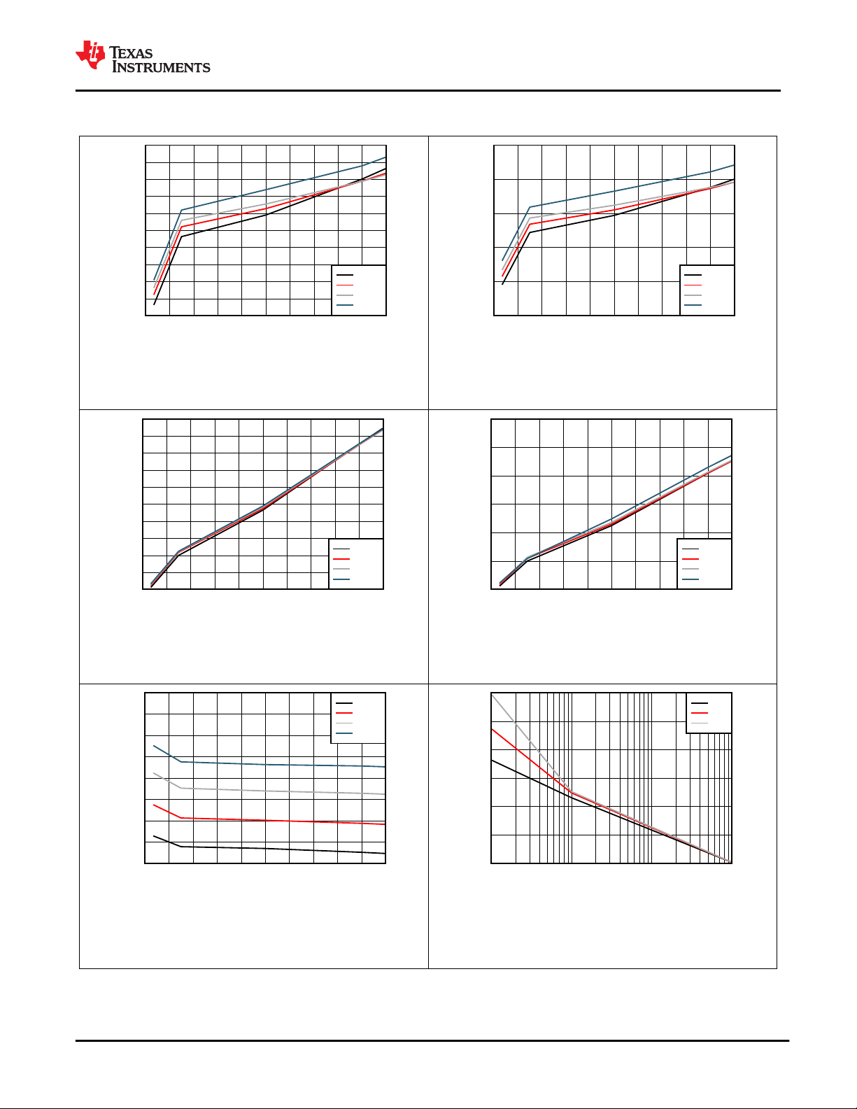
7.6 Typical Characteristics
SLVSEA3F – AUGUST 2018 – REVISED AUGUST 2020
TPS2120, TPS2121
ILM = 5.2A
Figure 7-1. Quiescent Current vs Input Voltage
ILM = 5.2A
Figure 7-3. Standby Current vs Input Voltage
ILM = 1.5A
Figure 7-2. Quiescent Current vs Input Voltage
ILM = 1.5A
Figure 7-4. Standby Current vs Input Voltage
I
= -200 mA
OUT
Figure 7-5. TPS2121 On-Resistance vs Input
Voltage
Copyright © 2020 Texas Instruments Incorporated
V
> UVLO V
IN1
Figure 7-6. Output Slew Rate vs CSS Capacitor
Product Folder Links: TPS2120 TPS2121
= 0V
IN2
Submit Document Feedback
9
TPS2120, TPS2121
SLVSEA3F – AUGUST 2018 – REVISED AUGUST 2020
V
= 12 V V
IN1
IN2
= 0 V
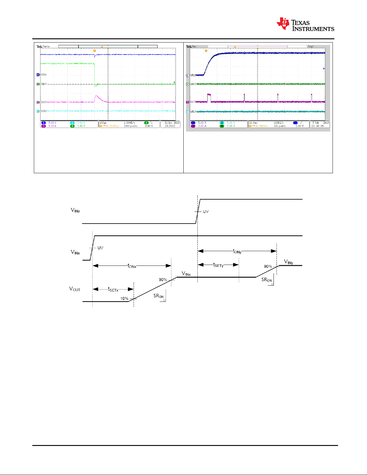
Figure 7-7. TPS2121 Hot Short on OUT while IN1 is
Enabled
8 Parameter Measurement Information
www.ti.com
V
= 12 V V
IN1
R
= 71.5kΩ
ILM
= 0 V V
IN2
OUT
= GND
Figure 7-8. TPS2120 IN1 is Enabled with a Short on
OUT
10 Submit Document Feedback
Figure 8-1. Timing Parameter Diagram
Copyright © 2020 Texas Instruments Incorporated
Product Folder Links: TPS2120 TPS2121
+
±
V
REF
Control Logic
+ Gate Drivers
+
±
+
±
+
±
Temp
SNS
Current
Limit
V
REF
V
REF
V
REF
Temp
SNS
BFET1 HFET1
BFET2 HFET2
IN1
PR1
SEL
OV1
OV2
IN2
ST
GND
SS
OUT
ILM
www.ti.com
SLVSEA3F – AUGUST 2018 – REVISED AUGUST 2020
9 Detailed Description
9.1 Overview
The TPS212x devices are Dual-Input, Single-Output (DISO) Power Multiplexer (MUX) that are well suited for a
variety of systems having multiple power sources. The devices will automatically detect, select, and seamlessly
transition between available inputs. Priority can be automatically given to the highest input voltage or manually
assigned to a lower voltage input to support both ORing and Source Selection operations. A priority voltage
supervisor is used to select an input source.
An Ideal Diode operation is used to seamlessly transition between input sources. During switchover, the voltage
drop is controlled to block reverse current before it happens and provide uninterrupted power to the load with
minimal hold-up capacitance. Active current limiting is used during startup and switchover to protect against
overcurrent, and also protects the device during normal operation. The output current limit can be adjusted with
a single external resistor.
9.2 Functional Block Diagram
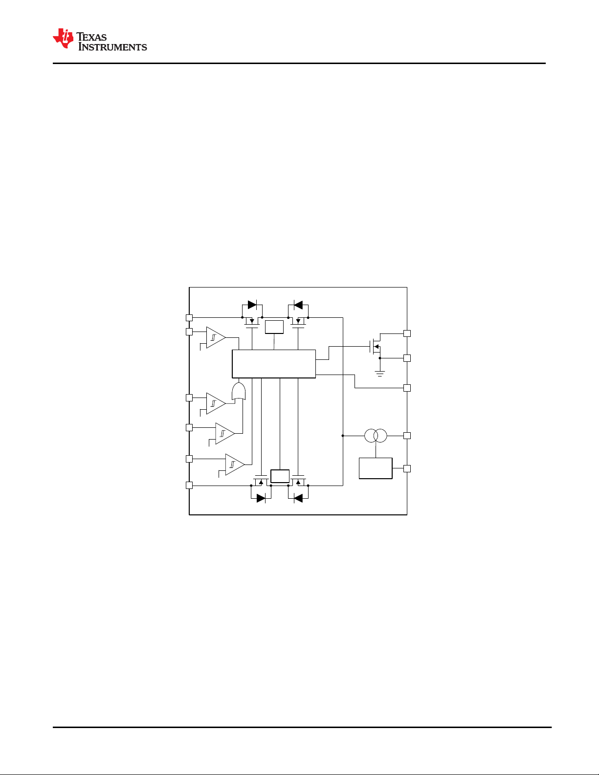
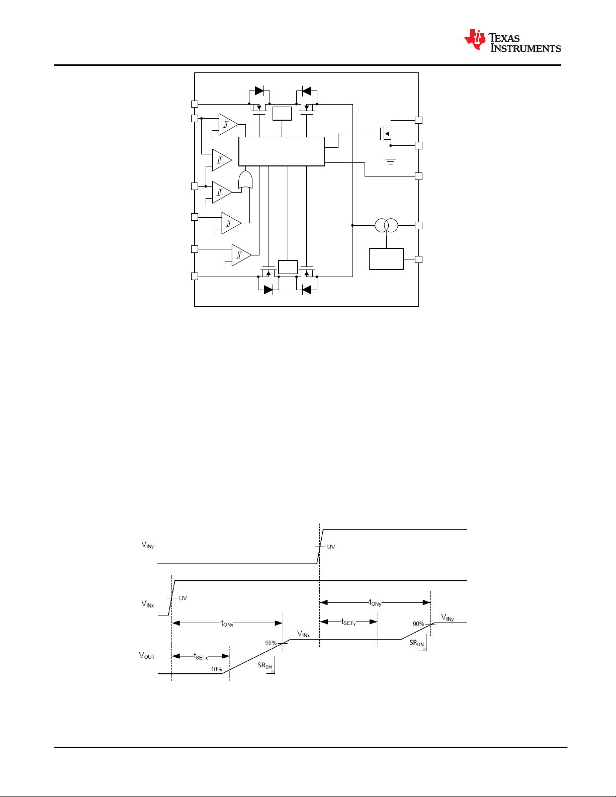
The below figures show the block diagrams for the TPS2120 and TPS2121. The TPS2120 has the SEL pin,
while the TPS2121 has the CP2 pin and supports fast switchover.
TPS2120, TPS2121
Figure 9-1. TPS2120 Functional Block Diagram
Copyright © 2020 Texas Instruments Incorporated
Product Folder Links: TPS2120 TPS2121
Submit Document Feedback
11
+
±
V
REF
Control Logic
+ Gate Drivers
+
±
+
±
+
±
Temp
SNS
Current
Limit
V
REF
V
REF
V
REF
Temp
SNS
BFET1 HFET1
BFET2 HFET2
IN1
PR1
CP2
OV1
OV2
IN2
ST
GND
SS
OUT
ILM
+
±
V
OFST
TPS2120, TPS2121
SLVSEA3F – AUGUST 2018 – REVISED AUGUST 2020
Figure 9-2. TPS2121 Functional Block Diagram
www.ti.com
9.3 Feature Description
This section describes the different features of the TPS212x power mux device.
9.3.1 Input Settling Time and Output Soft Start Control (SS)
The TPS212x will automatically select the first source to become valid (INx >UV and INx <OV). The external
capacitor (CSS) will then be used as a timer to wait for the input to finish setting (tSETx). When the settling timer
has expired, CSS will continue to charge and set the output slew rate (SRON) for a soft start. After the total turn
on time (tONx), soft start will not be used again for INx until it ceases to be valid (INx <UV or INx >OV).
When the second source becomes valid (INy >UV and INy <OV), the external capacitor (Css) will be used again
for a second settling time (tSETy). After tSETy, the TPS212x will decide whether to continue sourcing the first
source, or switchover to the second source. If the second source is selected at the end of tSETy, then CSS will
be reused to set the output slew rate (SRON) for a second soft start. After the total turn on time (tONy), soft start
will not be used again for INy until it ceases to be valid (INy <UV or INy >OV).
If INy becomes valid before the end of tONx, tSETy will be delayed and start after tONx has ended.
12 Submit Document Feedback
Figure 9-3. Settling and Soft Start Timing
Product Folder Links: TPS2120 TPS2121
Copyright © 2020 Texas Instruments Incorporated

LM
0.861
ILM
69.1
IR
LM
0.861
ILM
65.2
IR
www.ti.com
SLVSEA3F – AUGUST 2018 – REVISED AUGUST 2020
If INy is not selected during tSETy, a second soft start will not take place, skipping tONy, and CSS will be retired
until one of the inputs ceases to be valid.
9.3.1.1 Slew Rate vs. CSS Capacitor
Table 9-1 shows the estimated slew rate across CSS capacitance and VIN.
Table 9-1. Slew Rate vs. CSS Capacitor
TPS2120, TPS2121
CSS CAPACITOR VIN = 5 V VIN = 12 V VIN = 20 V UNITS
100 nF 780 800 880 V/s
1 uF 88 92 92 V/s
10 uF 8.8 9.6 10.4 V/s
9.3.2 Active Current Limiting (ILM)
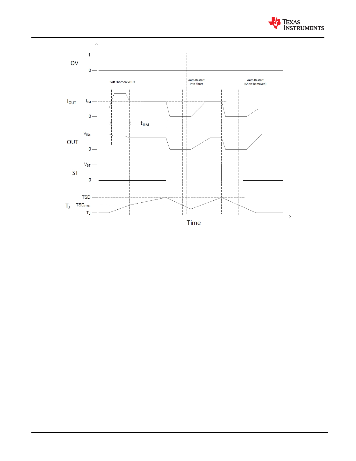
The load current is monitored at all times. When the load current exceed the current limit trip point ILM
programmed by RILM resistor, the device regulates the current within t
. The following equations can be used
ILM
to find the RILM value for a desired current limit, where RILM is in kΩ and between 18 kΩ to 100 kΩ.
TPS2120:
TPS2121:
(1)
(2)
During current regulation, the output voltage will drop resulting in increased device power dissipation. If the
device junction temperature (TJ) reaches the thermal shutdown threshold (TSD) the internal FETs are turned off.
After cooling down, the device will automatically restart.
Copyright © 2020 Texas Instruments Incorporated
Product Folder Links: TPS2120 TPS2121
Submit Document Feedback
13
TPS2120, TPS2121
SLVSEA3F – AUGUST 2018 – REVISED AUGUST 2020
www.ti.com
Figure 9-4. Current Limiting Behavior
9.3.3 Short-Circuit Protection
During a transient short circuit event, the current through the device increases very rapidly. As the current-limit
amplifier cannot respond quickly to this event due to its limited bandwidth, the device incorporates a fast-trip
overcurrent protection (OCP) comparator, with a threshold I
within 1 µs, when the current through internal FET IOUT exceeds I
about 2.4x of the programmed current limit I
= 2.4 × ILM. The OCP circuit holds the internal FET off for about
OCP
. This comparator shuts down the pass device
OCP
(I
> I
OCP
OUT
). The trip threshold is set to
OCP
25 ms, after which the device turns back on. If the short is still present then the current-limit loop will regulate the
output current to ILM and behave in a manner similar to a power up into a short.
9.3.4 Thermal Protection (TSD)
The TPS212x devices have built-in absolute thermal shutdown and relative thermal shutdown to ensure
maximum reliability of the power mux. The absolute thermal shutdown is designed to disable the power FETs, if
the junction temperature exceeds 160°C (typical). The device auto recovers about 25 ms after TJ < [T (TSD) –
10°C]. The relative thermal shutdown protects the device by turning off when the temperature of the power FETs
increases sharply such that the FET temperature rises about 60°C above the rest of the die. The device auto
recovers about 25 ms after the FETs cools down by 20°C. The relative thermal shutdown is critical for protecting
the device against faults such as a power up into a short which causes the FET temperature to increase sharply.
9.3.5 Overvoltage Protection (OVx)
Output Overvoltage Protection is available for both IN1 and IN2 in case either applied voltage is greater than the
maximum supported load voltage. The VREF comparator on the OVx pins allow for the Overvoltage Protection
threshold to be adjusted independently for each input. When overvoltage is engaged, the corresponding channel
will turn off immediately. Fast switchover to the other input is supported if it is a valid voltage.
14 Submit Document Feedback
Copyright © 2020 Texas Instruments Incorporated
Product Folder Links: TPS2120 TPS2121
 Loading...