

Page 1

User's Guide
SLVUBD2A–September 2018–Revised January 2019
TPS212x Evaluation Module
This user's guide describes the characteristics, operation, and use of the TPS212xEVM (EVM). This
document contains the EVM schematics, board layout, bill of materials (BOM), and necessary instructions
on how to properly operate the EVM.
Contents
1 Introduction ................................................................................................................... 2
2 General Configurations ..................................................................................................... 3
3 Test Setup and Results ..................................................................................................... 6
4 Board Layout ................................................................................................................. 7
5 Schematic..................................................................................................................... 9
6 Bill of Materials ............................................................................................................. 11
List of Figures
1 TPS2121 Setup With Test Equipment ................................................................................... 7
2 TPS2120 Setup With Test Equipment .................................................................................... 8
3 TPS2121 Schematic......................................................................................................... 9
4 TPS2120 Schematic ....................................................................................................... 10
1 TPS212x EVM Comparison Table......................................................................................... 2
2 TPS2121 Input and Output Connector Functionality.................................................................... 3
3 TPS2121 Test Points Description ......................................................................................... 3
4 TPS2121 Jumper Description.............................................................................................. 3
5 TPS2120 Input and Output Connector Functionality.................................................................... 4
6 TPS2120 Test Points Description ......................................................................................... 4
7 TPS2120 Jumper Description.............................................................................................. 5
8 Default Jumper Settings for TPS2121 Evaluation Board............................................................... 6
9 Default Jumper Settings for TPS2120 Evaluation Board............................................................... 6
10 TPS2121EVM-023 Bill of Materials ..................................................................................... 11
11 TPS2120EVM-042 Bill of Materials ..................................................................................... 13
Trademarks
All trademarks are the property of their respective owners.
List of Tables
SLVUBD2A–September 2018–Revised January 2019
Submit Documentation Feedback
Copyright © 2018–2019, Texas Instruments Incorporated
TPS212x Evaluation Module
1
Page 2

Introduction
1 Introduction
The TPS212x EVM is an evaluation module for TI's TPS212x family of two-input, one-output power
multiplexers. This device automatically detects, selects, and seamlessly transitions between two power
supplies, each operating from 2.7 V to 22 V. The TPS2121 device, the VSON hot-rod package, can deliver
up to 4 A while the TPS2120, WCSP package, can handle up to 3 A. This user's guide contains the EVM
schematics, board layout, list of materials, and necessary instructions on how to properly operate the
EVM.
The EVM has test points for convenient access to all critical voltages and pins, and jumpers to configure
the different modes of operation. There are also jumpers to configure input and output capacitance, output
load resistance, current limit, and the adjustable soft-start time.
1.1 Features
The TPS212x EVM offers many features including:
• Uninterrupted system power with seamless switchover
• Overvoltage protection
• Low RONresistance at both inputs: 50 mΩ typical
• Multiple configurations for different modes of operation
1.2 Applications
The TPS212x power multiplexer can be used in many applications, including:
• Add-on cards (PCIE, RAID, Network)
• ePos
• Video surveillance
• ORing controllers
www.ti.com
1.3 Description
The TPS212x EVM power MUX evaluation board enables evaluation of the TPS212x family of Power
MUX devices. Although both variants (TPS2121EVM-042 or TPS2120EVM-023) contain different jumpers
and connectors, they will function almost identically. Both EVMs allow operation at different input voltages,
although the resistors and jumpers are configured for operation at 3.3 V, 5 V, and 12 V. See the TPS212x
data sheet for more information regarding these settings.
The TPS212x EVMs also allow multiple modes of operation. By configuring the jumpers, the EVMs
automatically detect, select, and seamlessly transition between available inputs. The different modes of
operation are explained in Table 1.
EVM Modes of Operation: V
TPS2121EVM
TPS2120EVM
• VCOMP
• VREF
• XCOMP
• XREF
• VCOMP
• VREF
Table 1. TPS212x EVM Comparison Table
Range I
OUT
2.7 V–22 V 4 A VSON, 2.0 mm × 2.5 mm
2.7 V–22 V 3 A WCSP, 1.5 mm × 2.0 mm
MAX Package
OUT
2
TPS212x Evaluation Module
Copyright © 2018–2019, Texas Instruments Incorporated
SLVUBD2A–September 2018–Revised January 2019
Submit Documentation Feedback
Page 3
www.ti.com
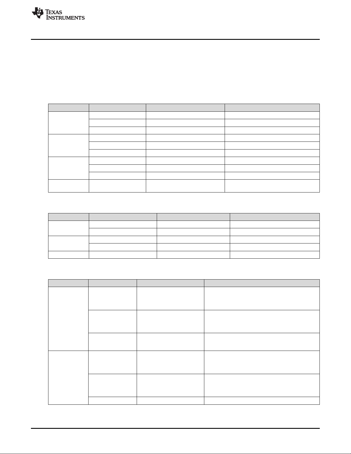
2 General Configurations
2.1 TPS2121 Configurations
This section provides an overview of the TPS212x evaluation board input and output jumpers. Table 2
describes the input and output connectors on the EVM. Table 3 describes the different test points and
functionality, while Table 4 describes the jumper functionality and configurations.
Table 2. TPS2121 Input and Output Connector Functionality
Input Connector Label Description
J21 VIN1 + , GND - Input block header for VIN1
VIN1
VIN2
VOUT
GND
TP12, TP13, TP14, TP15,
TP16, TP17, TP18, TP19
TP8 VIN1 Input test point for VIN1
TP6 VIN1_SNS Input sense connector for VIN1
J14 VIN2 + , GND - Input block header for VIN2
TP11 VIN2 Input test point for VIN2
TP6 VIN2_SNS Input sense connector for VIN2
J15 VOUT +, GND - Output block header for VOUT
TP9 VOUT Output test point for VOUT
TP7 VOUT_SNS Output sense connector for VOUT
General Configurations
GND Test point for GND
Table 3. TPS2121 Test Points Description
Input Connector Label Description
VIN1
VIN2
VOUT TP5 ST Status test point
TP1 OV1 Overvoltage test point for VIN1
TP4 PR1 Priority test point for VIN1
TP2 OV2 Overvoltage test point for VIN2
TP3 CP2 Comparator test point for VIN2
Table 4. TPS2121 Jumper Description
Input Connector Label Description
Sets priority operation based on voltage
J1 sets 3.3 V
J2 sets 5 V
J3 sets 12 V
Sets overvoltage protection for VIN1
J4 sets 3.3 V
J5, sets 5 V
J6 sets 12 V
Priority operation control
Position 1-2 sets VCOMP (GND)
Position 2-3 sets VREF, XCOMP, XREF
Sets XCOMP operation based on voltage
J7 sets 3.3 V
J8 sets 5 V
J9 sets 12 V
Sets overvoltage protection for VIN2 channel
J10 sets 3.3 V
J11, sets 5 V
J12 sets 12 V
VIN1
VIN2
J1, J2, J3
J4, J5, J6
JP1 PR1
J7, J8, J9
J10, J11, J12
J13 CP2 CP2 enable, disable
PR1 Resistors (3.3 V, 5 V, 12
V)
OV1 Resistors (3.3 V, 5 V, 12
V)
CP2 Resistors (3.3 V, 5 V, 12
V)
OV2 Resistors (3.3 V, 5 V, 12
V)
SLVUBD2A–September 2018–Revised January 2019
Submit Documentation Feedback
Copyright © 2018–2019, Texas Instruments Incorporated
TPS212x Evaluation Module
3
Page 4
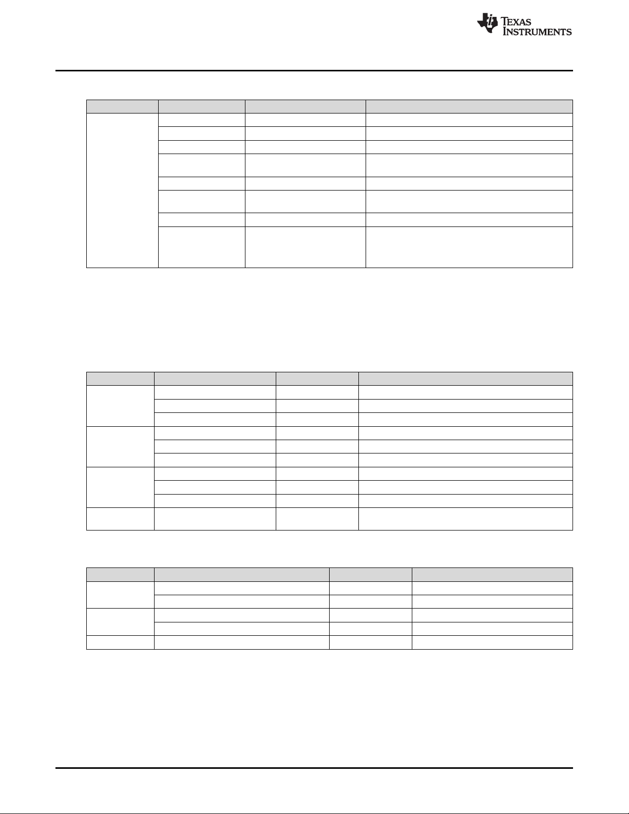
General Configurations
Table 4. TPS2121 Jumper Description (continued)
Input Connector Label Description
J17, J18 100 µF 100-µF output capacitor
J19 100 µF 100-µF output capacitor
J19 220 µF 220-µF output capacitor
J16 -
VOUT
J20 10 Ω 10-Ω external resistor
JP2 ST
J22, J23 SS Soft-start control
JP3 ILIM
2.2 TPS2120 Configurations
This section provides an overview of the TPS212x evaluation board input and output jumpers. Table 2
describes the input and output connectors on the EVM. Table 3 describes the different test points and
functionality, while Table 4 describes the jumper functionality and configurations.
Table 5. TPS2120 Input and Output Connector Functionality
www.ti.com
Female header for custom output resistance,
capacitance
Sets adjustable hysteresis
Position 1-2 sets ST, 2-3 disables (GND)
Current limit control
Position 1-2 position sets 4.5 A maximum
Position 2-3 sets 2 A maximum
No jumper sets 1.5 A maximum
Input Connector Label Description
J10 VIN1 + , GND - Input block header for VIN1
VIN1
VIN2
VOUT
GND
TP12, TP13, TP14, TP15,
TP16, TP17, TP18, TP19
TP7 VIN1 Input test point for VIN1
TP5 VIN1_SNS Input sense connector for VIN1
J17 VIN2 + , GND - Input block header for VIN2
TP11 VIN2 Input test point for VIN2
TP10 VIN2_SNS Input sense connector for VIN2
J11 VOUT +, GND - Output block header for VOUT
TP8 VOUT Output test point for VOUT
TP6 VOUT_SNS Output sense connector for VOUT
GND Test point for GND
Table 6. TPS2120 Test Points Description
Input Connector Label Description
VIN1
VIN2
VOUT TP4 ST Status test point
TP1 OV1 Overvoltage test point for VIN1
TP3 PR1 Priority test point for VIN1
TP2 OV2 Overvoltage test point for VIN2
TP9 SEL Select test point
4
TPS212x Evaluation Module
Copyright © 2018–2019, Texas Instruments Incorporated
SLVUBD2A–September 2018–Revised January 2019
Submit Documentation Feedback
Page 5
www.ti.com
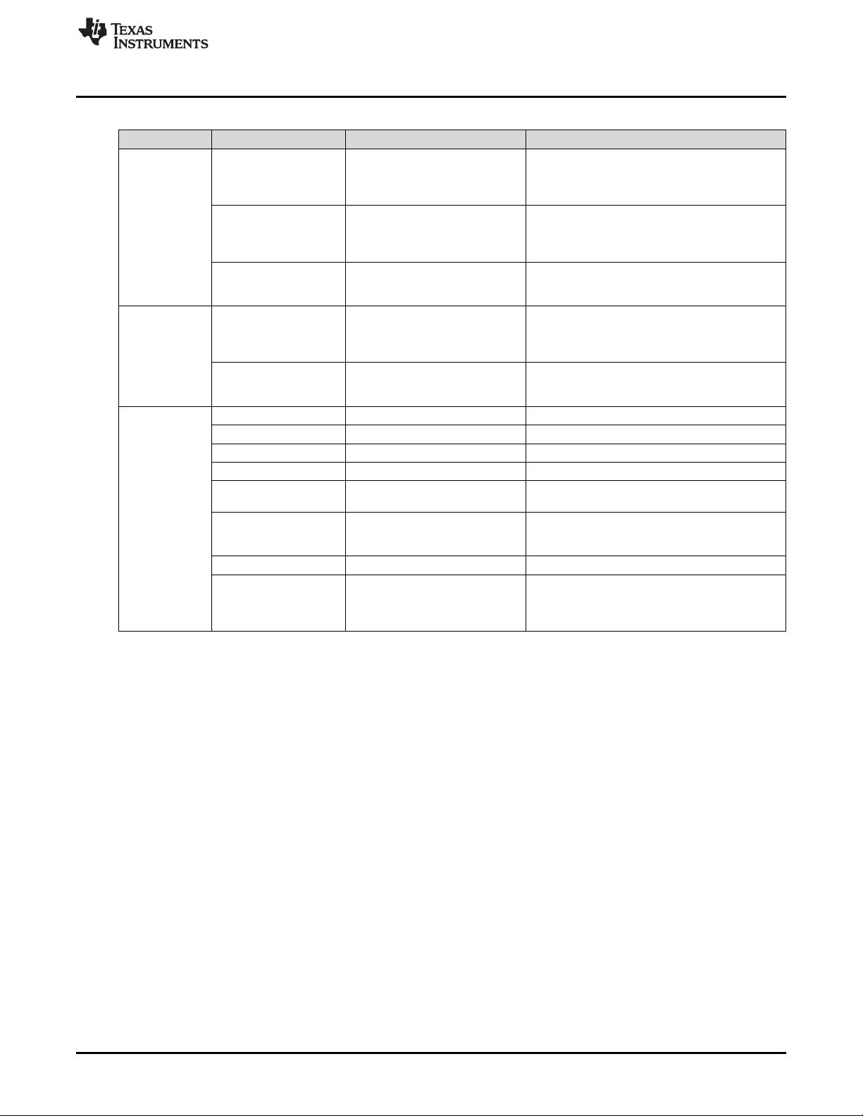
General Configurations
Table 7. TPS2120 Jumper Description
Input Connector Label Description
VIN1
VIN2
VOUT
Sets priority operation based on voltage
J1, J2, J3 PR1 Resistors (3.3 V, 5 V, 12 V)
Sets overvoltage protection for VIN1 channel
J4, J5, J6 OV1 Resistors (3.3 V, 5 V, 12 V)
JP2 PR1
J7, J8, J9 OV2 Resistors (3.3 V, 5 V, 12 V)
JP1 SEL
J12 100 µF 100-µF output capacitor
J13 100 µF 100-µF output capacitor
J14 220 µF 220-µF output capacitor
J15 10 Ω 10-Ω external resistor
J16 -
JP3 ST
J18, J19 SS Soft-start control
JP4 ILIM
Position 1-2 sets VCOMP (GND)
Sets overvoltage protection for VIN2 channel
Selects between priority control or GND
Female header for custom output resistance,
Position 1-2 sets 4.5 A maximum
J1 sets 3.3 V
J2 sets 5 V
J3 sets 12 V
J4 sets 3.3 V
J5, sets 5 V
J6 sets 12 V
Priority operation control
Position 2-3 sets VREF
J10 sets 3.3 V
J11, sets 5 V
J12 sets 12 V
Position 1-2 disables priority
Position 2-3 enables priority
capacitance
Sets adjustable hysteresis
Position 1-2 sets ST
Position 2-3 disables (GND)
Current Limit Control
Position 2-3 sets 2 A
No jumper sets 1.5 A
SLVUBD2A–September 2018–Revised January 2019
Submit Documentation Feedback
Copyright © 2018–2019, Texas Instruments Incorporated
TPS212x Evaluation Module
5
Page 6
Test Setup and Results
3 Test Setup and Results
This chapter describes the proper setup for the TPS212x power MUX EVM. This section explains the
different configuration modes present on each EVM, and the required jumper positions to enable each
configuration.
3.1 TPS212x EVM Test Equipment
Read the TPS212x data sheet before using the EVM.
The following test equipment is recommended:
• Storage oscilloscope
• Current problem
• Two adjustable power supples, 0 V–22 V at 4 A maximum
• A passive or active load
3.2 Setting up the TPS2121 EVM
Make sure the TPS2121 evaluation board has the default jumper settings as Table 8 shows.
Table 8. Default Jumper Settings for TPS2121 Evaluation Board
Input Connector Label Position
VIN1
VIN2
VOUT
J1 PR1 (3.3 V) Install
J4 OV1 (3.3 V) Install
J12 OV2 (12 V) Install
J13 CP2 Install
J17, J18 100 µF Install
J20 10 Ω Install
J22 SS (10 nF) Install
JP1 PR1 Jump pins 2 and 3
JP2 ST Jump pins 2 and 3
JP3 ILIM (4.5 A maximum) Jump pins 1 and 2
www.ti.com
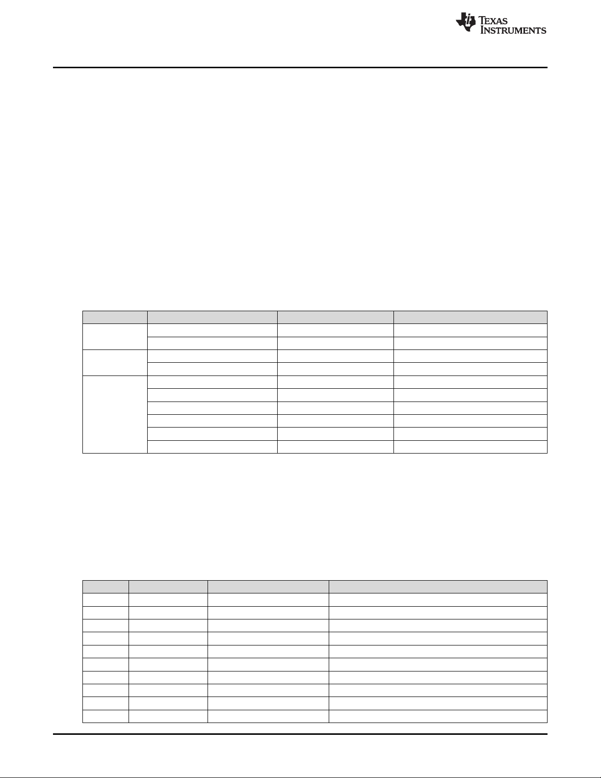
The default jumper configuration sets the Internal Voltage Reference (VREF) configuration. Since the
voltage on the priority pin is set for 3.3-V operation and CP2 is grounded, priority will be given to VIN1.
Therefore, VIN1 can be set to 3.3 V, and the device will prioritize VIN1 even if VIN2 is at a higher voltage.
See the data sheet for more information regarding the configuration settings.
3.3 Setting up the TPS2120 EVM
Make sure the TPS2120 evaluation board has default jumper settings as Table 9 shows.
Table 9. Default Jumper Settings for TPS2120 Evaluation Board
Input Connector Label Position
J1 PR1 (3.3 V) Install
J4 OV1 (3.3 V) Install
J9 J9 (12 V) Install
J12, J13 100 µF Install
J15 10 Ω Install
J18 SS (10 nF) Install
JP1 SEL Jump pins 1 and 2
JP2 PR1 Jump pins 2 and 3
JP3 ST Jump pins 2 and 3
JP4 ILIM (4.5 A maximum) Jump pins 2 and 3
6
TPS212x Evaluation Module
Copyright © 2018–2019, Texas Instruments Incorporated
SLVUBD2A–September 2018–Revised January 2019
Submit Documentation Feedback
Page 7
www.ti.com
The default jumper configuration sets the Internal Voltage Reference (VREF) configuration. Since the
voltage on the priority pin is set for 3.3-V operation and SEL is grounded, the priority is given to VIN1.
Therefore, VIN1 can be set to 3.3 V, and the device will prioritize VIN1 even if VIN2 is at a higher voltage.
See the data sheet for more information regarding the configuration settings.
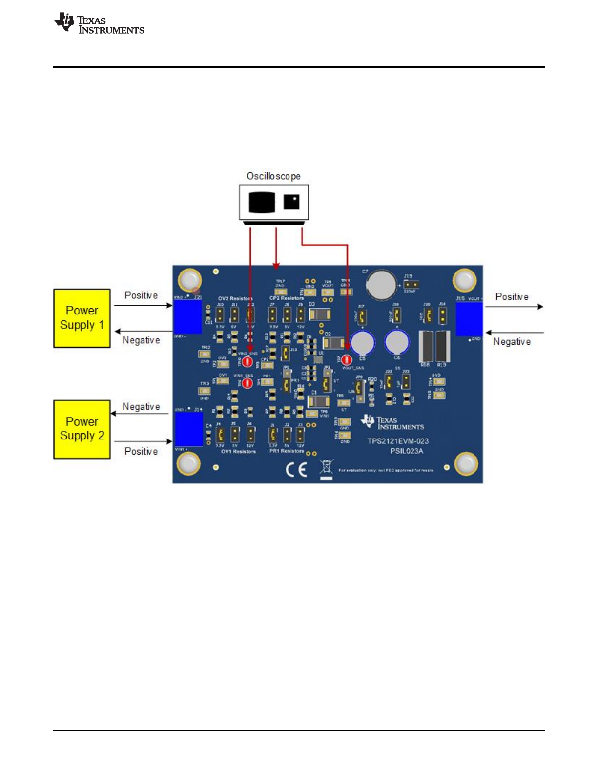
4 Board Layout
Figure 1 and Figure 2 show the test equipment setup for the TPS2121 and TPS2120, respectively.
Board Layout
Figure 1. TPS2121 Setup With Test Equipment
SLVUBD2A–September 2018–Revised January 2019
Submit Documentation Feedback
Copyright © 2018–2019, Texas Instruments Incorporated
TPS212x Evaluation Module
7
Page 8

Board Layout
www.ti.com
Figure 2. TPS2120 Setup With Test Equipment
8
TPS212x Evaluation Module
Copyright © 2018–2019, Texas Instruments Incorporated
SLVUBD2A–September 2018–Revised January 2019
Submit Documentation Feedback
Page 9

J14
1
2
J15
VIN1
2.7V to 22V
GND
VOUT
4A Max
GND
VOUTVIN1
J21
VIN2
2.7V to 22V
GND
GND
OV1 Resistors
GND
1
2
3
JP1
GND
1
2
3
JP2
GND
PR1 Resistors
VIN1
PR1
VIN2
ST Connector
5k
R13
GND
OV2 Resistors
GND
OV2
CP2
OV2
PR1_TP
ST_TP
OV1_TP OV2_TP
VIN2
GND
GND GND
1
2
3
JP3
GND
GND
GND
GND
Cout Capacitors Rout Resistors Female Header
Vout
1
2
J16
XREF/CP2_TP
ST
Recommended input voltages:
3.3V 5V 12V 3.3V 5V 12V
3.3V 5V 12V 3.3V 5V 12V
CP2 Resistors
0.1uF
C3
0.1uF
C10
GND
GND
VIN1
GND GND GND GND GND GND GND GND
GND
GND
20V
D1
20V
D3
0.1uF
C4
0.1uF
C11
10.2k
R7
10.2k
R10
18.2k
R8
18.2k
R11
13.7k
R1
23.7kR263.4k
R3
5.00k
R14
OV1
13.7k
R4
23.7kR563.4k
R6
5.00k
R17
0.01uF
C12
1uF
C13
TP1
TP4
TP5
TP8
TP11
TP9
TP12 TP13 TP14 TP15 TP16 TP17 TP18 TP19
TP3
TP2
TP6
TP10
TP7
5.00k
R15
GND
GND
IN1
7
OUT
1
ST
9
ILM
10
SS
11
GND
12
OUT
8
IN2
2
CP2
3
OV2
4
OV1
5
PR1
6
TPS2121RUXR
U1
OV1
ST
PR1
CP2
20V
D2
GND
100uF
C5
220uF
C7
GND
100uF
C6
GND
0.1uF
C1
GND GND
0.1uF
C2
0.1uF
C8
GND GND
0.1uF
C9
51.1k
R20
21.5k
R21
5
R18
5
R19
3.3V, 5V, and 12V @ 4A Imax
J1 J2 J3 J4 J5 J6 J7 J8 J9 J10 J11 J12
J13
J17 J18 J19 J20
J22 J23
Maximum Output Voltage: 22V
PR1
ILIM
49.9k
R9
49.9k
R12
10.7k
R16
www.ti.com
5 Schematic
Figure 3 illustrates the TPS2121 schematic and Figure 4 illustrates the TPS2120 schematic.
Schematic
SLVUBD2A–September 2018–Revised January 2019
Submit Documentation Feedback
Figure 3. TPS2121 Schematic
Copyright © 2018–2019, Texas Instruments Incorporated
TPS212x Evaluation Module
9
Page 10

J10
1
2
J11
VIN1
2.7V to 22V
GND
VOUT
4A Max
GND
VOUTVIN1
J17
VIN2
2.7V to 22V
GND
GND
OV1 Resistors
GND
1
2
3
JP2
GND
1
2
3
JP3
GND
PR1 Resistors
VIN1
PR1
VIN2
ST Connector
5k
R10
GND
OV2 Resistors
GND
OV2
OV2
PR1_TP
ST_TP
OV1_TP
OV2_TP
VIN2
GND
GND GND
1
2
3
JP4
GND
GND
GND
GND
Cout Capacitors Rout Resistors Female Header
Vout
1
2
J16
ST
Recommended input voltages:
3.3V 5V 12V 3.3V 5V 12V
3.3V 5V 12V
0.1uF
C4
0.1uF
C11
GND
GND
VIN1
GND GND GND GND GND GND GND GND
GND
GND
20V
D1
20V
D3
0.1uF
C5
0.1uF
C12
10.2k
R7
18.2k
R8
13.7k
R1
23.7kR263.4k
R3
5.00k
R11
OV1
13.7k
R4
23.7kR563.4k
R6
0.01uF
C13
1uF
C14
TP1
TP3
TP4
TP7
TP11
TP8
TP12 TP13 TP14 TP15 TP16 TP17 TP18 TP19
TP2
TP5
TP10
TP6
5.00k
R12
GND
GND
OV1
ST
PR1
20V
D2
GND
100uF
C6
220uF
C8
GND
100uF
C7
GND
0.1uF
C2
GND GND
0.1uF
C3
0.1uF
C9
GND GND
0.1uF
C10
51.1k
R17
21.5k
R18
5
R15
5
R16
3.3V, 5V, and 12V @ 3A Imax
IN1
B1
OUT
C3
ST
E1
ILM
E2
SS
E3
GND
E4
OUT
C2
IN2
B3
IN1
B2
OV2
A3
OV1
A2
PR1
A1
IN1
C1
SEL
A4
IN2
B4
IN2
C4
OUT
D1
OUT
D2
OUT
D3
OUT
D4
TPS2120YFPR
U1
SEL
1
2
3
JP1
0.1uF
C110.0k
R14
GND
SEL
PR1
Select
TP9
Maximum Output Voltage: 22V
J1 J2 J3 J4 J5 J6 J7 J8 J9
J18 J19
J12 J13 J14 J15
PR1
ILIM
49.9k
R9
10.7k
R13
Schematic
www.ti.com
SLVUBD2A–September 2018–Revised January 2019
Submit Documentation Feedback
Figure 4. TPS2120 Schematic
Copyright © 2018–2019, Texas Instruments Incorporated
10
TPS212x Evaluation Module
Page 11

www.ti.com
6 Bill of Materials
Table 10 lists the TPS2121EVM-023 BOM and Table 11 lists the TPS2120EVM-042 BOM.
Bill of Materials
Table 10. TPS2121EVM-023 Bill of Materials
Designator Quantity Value Description PackageReferencePartNumber Manufacturer Alternate
!PCB1 1 Printed Circuit
C1, C2, C3, C4,
C8, C9, C10, C11
C5,C6 2 100uF CAP, AL, 100 uF,
C7 1 220uF CAP, AL, 220 uF,
C12 1 0.01uF CAP, CERM, 0.01
C13 1 1uF CAP, CERM, 1 uF,
D1, D2, D3 3 20V Diode, TVS, Uni,
H1, H2, H3, H4 4 Machine Screw,
H5, H6, H7, H8 4 Standoff, Hex,
J1, J2, J3, J4, J5,
J6, J7, J8, J9, J10,
J11, J12, J13, J17,
J18, J19, J20, J22,
J23
J14, J15, J21 3 Terminal Block,
J16 1 Receptacle, 2x1,
JP1, JP2, JP3 3 Header, 100mil,
8 0.1uF CAP, CERM, 0.1
19 Header, 100mil,
Board
uF, 25 V, +/- 10%,
X7R, 0603
50 V, +/- 20%, 0.17
ohm, TH
35 V, +/- 20%, TH
uF, 50 V, +/- 10%,
X7R, 0805
50 V, +/- 10%,
X7R, 0805
20 V, 32.4 Vc,
SMB
Round, #4-40 x
1/4, Nylon, Philips
panhead
0.5"L #4-40 Nylon
2x1, Gold, TH
2x1, 5.08mm, TH
2.54mm, Tin, TH
3x1, TH
0603 06033C104KAT2A AVX
8.0x10.5mm UHE1H101MPD Nichicon
D10xL12.5mm UHE1V221MPD6 Nichicon
0805 885012207092 Wurth Elektronik
0805 C0805C105K5RACTUKemet
SMB SMBJ20A-13-F Diodes Inc.
Screw NY PMS 440 0025PHB&F Fastener
Standoff 1902C Keystone
2x1 Header TSW-102-07-G-S Samtec
2x1 Terminal Block OSTTA024163 On-Shore
Receptacle, 2x1,
2.54mm, TH
Header, 3x1,
100mil, TH
PSIL023 Any
SSW-102-01-T-S Samtec
800-10-003-10001000
(1)
PartNumber
Supply
Technology
Mill-Max
Alternate
Manufacturer
(1)
Unless otherwise noted in the Alternate Part Number or Alternate Manufacturer columns, all parts may be substituted with equivalents.
SLVUBD2A–September 2018–Revised January 2019
Submit Documentation Feedback
Copyright © 2018–2019, Texas Instruments Incorporated
TPS212x Evaluation Module
11
Page 12

Bill of Materials
www.ti.com
Table 10. TPS2121EVM-023 Bill of Materials
R1, R4 2 13.7k RES, 13.7 k, 1%,
R2, R5 2 23.7k RES, 23.7 k, 0.1%,
R3, R6 2 63.4k RES, 63.4 k, 0.1%,
R7, R10 2 10.2k RES, 10.2 k, 0.5%,
R8, R11 2 18.2k RES, 18.2 k, 0.1%,
R9, R12 2 49.9k RES, 49.9 k, 0.5%,
R13 1 5.00k RES, 5.00 k, 0.1%,
R14, R15, R17 3 5.00k RES, 5.00 k, 0.1%,
R16 1 10.7k RES, 10.7 k, 1%,
R18, R19 2 5 RES, 5, 1%, 50 W,
R20 1 51.1k RES, 51.1 k, 0.5%,
R21 1 21.5k RES, 21.5 k, .5%,
SH-J1, SH-J2, SHJ3, SH-J4, SH-J5,
SH-J6, SH-J7, SHJ8, SH-J9, SH-J10,
SH-J11
TP1, TP2, TP3,
TP4, TP5, TP8,
TP9, TP11, TP12,
TP13, TP14, TP15,
TP16, TP17, TP18,
TP19
TP6, TP7, TP10 3 Test Point,
11 1x2 Shunt, 100mil,
16 Test Point,
0.125 W, 0805
0.125 W, 0805
0.1 W, 0603
0.1 W, 0805
0.125 W, 0805
0.1 W, 0805
0.05 W, 0402
0.2 W, 0805
0.125 W, AECQ200 Grade 0,
0805
TO-220-2
0.1 W, 0603
.0625 W, 0603
Flash Gold, Black
Miniature, SMT
Multipurpose, Red,
TH
(1)
(continued)
0805 ERJ-6ENF1372V Panasonic
0805 RT0805BRD0723K7LYageo America
0603 RT0603BRD0763K4LYageo America
0805 RR1220P-1022-D-MSusumu Co Ltd
0805 RT0805BRD0718K2LYageo America
0805 RR1220P-4992-D-MSusumu Co Ltd
0402 PNM0402E5001BST1Vishay-Dale
0805 PNM0805E5001BST5Vishay Thin Film
0805 CRCW080510K7F
TO-220-2 PF2205-5RF1 RIDEON
0603 RT0603DRE0751K1LYageo America
0603 RR0816P-2152-D-
Closed Top 100mil
Shunt
Testpoint_Keyston
e_Miniature
Red Multipurpose
Testpoint
KEA
33C
SPC02SYAN Sullins Connector
5015 Keystone
5010 Keystone
Vishay-Dale
Susumu Co Ltd
Solutions
12
TPS212x Evaluation Module
SLVUBD2A–September 2018–Revised January 2019
Submit Documentation Feedback
Copyright © 2018–2019, Texas Instruments Incorporated
Page 13

www.ti.com
Bill of Materials
Table 10. TPS2121EVM-023 Bill of Materials
U1 1 2.7V-22V, 4A,
RUX0012A TPS2121RUXR Texas Instruments TPS2121RUXT Texas Instruments
(1)
(continued)
50mohm Priority
Power MUX,
RUX0012A (VQFNHR-12)
FID1, FID2, FID3 0 Fiducial mark.
N/A N/A N/A
There is nothing to
buy or mount.
Table 11. TPS2120EVM-042 Bill of Materials
(1)
Designator Quantity Value Description PackageReferencePartNumber Manufacturer Alternate
PartNumber
!PCB1 1 Printed Circuit
PSIL042 Any
Board
C1, C2, C3, C4,
C5, C9, C10, C11,
C12
C6, C7 2 100uF CAP, AL, 100 uF,
9 0.1uF CAP, CERM, 0.1
uF, 25 V, +/- 10%,
X7R, 0603
0603 06033C104KAT2A AVX
8.0x10.5mm UHE1H101MPD Nichicon
50 V, +/- 20%, 0.17
ohm, TH
C8 1 220uF CAP, AL, 220 uF,
D10xL12.5mm UHE1V221MPD6 Nichicon
35 V, +/- 20%, TH
C13 1 0.01uF CAP, CERM, 0.01
0805 885012207092 Wurth Elektronik
uF, 50 V, +/- 10%,
X7R, 0805
C14 1 1uF CAP, CERM, 1 uF,
0805 C0805C105K5RACTUKemet
50 V, +/- 10%,
X7R, 0805
D1, D2, D3 3 20V Diode, TVS, Uni,
SMB SMBJ20A-13-F Diodes Inc.
20 V, 32.4 Vc,
SMB
H1, H2, H3, H4 4 Machine Screw,
Round, #4-40 x
Screw NY PMS 440 0025PHB&F Fastener
Supply
1/4, Nylon, Philips
panhead
H5, H6, H7, H8 4 Standoff, Hex,
Standoff 1902C Keystone
0.5"L #4-40 Nylon
J1, J2, J3, J4, J5,
J6, J7, J8, J9, J12,
15 Header, 100mil,
2x1, Gold, TH
2x1 Header TSW-102-07-G-S Samtec
J13, J14, J15, J18,
J19
Alternate
Manufacturer
(1)
Unless otherwise noted in the Alternate Part Number or Alternate Manufacturer columns, all parts may be substituted with equivalents.
SLVUBD2A–September 2018–Revised January 2019
Submit Documentation Feedback
Copyright © 2018–2019, Texas Instruments Incorporated
TPS212x Evaluation Module
13
Page 14

Bill of Materials
www.ti.com
Table 11. TPS2120EVM-042 Bill of Materials
J10, J11, J17 3 Terminal Block,
J16 1 Receptacle, 2x1,
JP1, JP2, JP3, JP4 4 Header, 100mil,
R1, R4 2 13.7k RES, 13.7 k, 1%,
R2, R5 2 23.7k RES, 23.7 k, 0.1%,
R3, R6 2 63.4k RES, 63.4 k, 0.1%,
R7 1 10.2k RES, 10.2 k, 0.5%,
R8 1 18.2k RES, 18.2 k, 0.1%,
R9 1 49.9k RES, 49.9 k, 0.5%,
R10 1 5.00k RES, 5.00 k, 0.1%,
R11, R12 2 5.00k RES, 5.00 k, 0.1%,
R13 1 10.7k RES, 10.7 k, 1%,
R14 1 10.0k RES, 10.0 k, 0.5%,
R15, R16 2 5 RES, 5, 1%, 50 W,
R17 1 51.1k RES, 51.1 k, 0.5%,
R18 1 21.5k RES, 21.5 k, .5%,
SH-J1, SH-J2, SHJ3, SH-J4, SH-J5,
SH-J6, SH-J7, SHJ8, SH-J9, SH-J10
10 1x2 Shunt, 100mil,
2x1, 5.08mm, TH
2.54mm, Tin, TH
3x1, TH
0.125 W, 0805
0.125 W, 0805
0.1 W, 0603
0.1 W, 0805
0.125 W, 0805
0.1 W, 0805
0.05 W, 0402
0.2 W, 0805
0.125 W, AECQ200 Grade 0,
0805
0.1 W, 0603
TO-220-2
0.1 W, 0603
.0625 W, 0603
Flash Gold, Black
(1)
(continued)
2x1 Terminal Block OSTTA024163 On-Shore
Receptacle, 2x1,
2.54mm, TH
Header, 3x1,
100mil, TH
0805 ERJ-6ENF1372V Panasonic
0805 RT0805BRD0723K7LYageo America
0603 RT0603BRD0763K4LYageo America
0805 RR1220P-1022-D-MSusumu Co Ltd
0805 RT0805BRD0718K2LYageo America
0805 RR1220P-4992-D-MSusumu Co Ltd
0402 PNM0402E5001BST1Vishay-Dale
0805 PNM0805E5001BST5Vishay Thin Film
0805 CRCW080510K7F
0603 RT0603DRE0710KLYageo America
TO-220-2 PF2205-5RF1 RIDEON
0603 RT0603DRE0751K1LYageo America
0603 RR0816P-2152-D-
Closed Top 100mil
Shunt
SSW-102-01-T-S Samtec
800-10-003-10-
001000
KEA
33C
SPC02SYAN Sullins Connector
Technology
Mill-Max
Vishay-Dale
Susumu Co Ltd
Solutions
14
TPS212x Evaluation Module
SLVUBD2A–September 2018–Revised January 2019
Submit Documentation Feedback
Copyright © 2018–2019, Texas Instruments Incorporated
Page 15

www.ti.com
Bill of Materials
Table 11. TPS2120EVM-042 Bill of Materials
TP1, TP2, TP3,
TP4, TP7, TP8,
TP9, TP11, TP12,
TP13, TP14, TP15,
TP16, TP17, TP18,
TP19
TP5, TP6, TP10 3 Test Point,
U1 1 TPS2120YFPR,
FID1, FID2, FID3 0 Fiducial mark.
16 Test Point,
Miniature, SMT
Multipurpose, Red,
TH
YFP0020AAAA
(DSBGA-20)
There is nothing to
buy or mount.
(1)
(continued)
Testpoint_Keyston
e_Miniature
Red Multipurpose
Testpoint
YFP0020AAAA TPS2120YFPR Texas Instruments TPS2120YFPT Texas Instruments
N/A N/A N/A
5015 Keystone
5010 Keystone
SLVUBD2A–September 2018–Revised January 2019
Submit Documentation Feedback
Copyright © 2018–2019, Texas Instruments Incorporated
TPS212x Evaluation Module
15
Page 16

Revision History
www.ti.com
Revision History
NOTE: Page numbers for previous revisions may differ from page numbers in the current version.
Changes from Original (September 2018) to A Revision ............................................................................................... Page
• Changes made in Table 4................................................................................................................ 3
• Changes made in the Bill of Materials table.......................................................................................... 11
16
Revision History
SLVUBD2A–September 2018–Revised January 2019
Copyright © 2018–2019, Texas Instruments Incorporated
Submit Documentation Feedback
Page 17

STANDARD TERMS FOR EVALUATION MODULES
1. Delivery: TI delivers TI evaluation boards, kits, or modules, including any accompanying demonstration software, components, and/or
documentation which may be provided together or separately (collectively, an “EVM” or “EVMs”) to the User (“User”) in accordance
with the terms set forth herein. User's acceptance of the EVM is expressly subject to the following terms.
1.1 EVMs are intended solely for product or software developers for use in a research and development setting to facilitate feasibility
evaluation, experimentation, or scientific analysis of TI semiconductors products. EVMs have no direct function and are not
finished products. EVMs shall not be directly or indirectly assembled as a part or subassembly in any finished product. For
clarification, any software or software tools provided with the EVM (“Software”) shall not be subject to the terms and conditions
set forth herein but rather shall be subject to the applicable terms that accompany such Software
1.2 EVMs are not intended for consumer or household use. EVMs may not be sold, sublicensed, leased, rented, loaned, assigned,
or otherwise distributed for commercial purposes by Users, in whole or in part, or used in any finished product or production
system.
2 Limited Warranty and Related Remedies/Disclaimers:
2.1 These terms do not apply to Software. The warranty, if any, for Software is covered in the applicable Software License
Agreement.
2.2 TI warrants that the TI EVM will conform to TI's published specifications for ninety (90) days after the date TI delivers such EVM
to User. Notwithstanding the foregoing, TI shall not be liable for a nonconforming EVM if (a) the nonconformity was caused by
neglect, misuse or mistreatment by an entity other than TI, including improper installation or testing, or for any EVMs that have
been altered or modified in any way by an entity other than TI, (b) the nonconformity resulted from User's design, specifications
or instructions for such EVMs or improper system design, or (c) User has not paid on time. Testing and other quality control
techniques are used to the extent TI deems necessary. TI does not test all parameters of each EVM.
User's claims against TI under this Section 2 are void if User fails to notify TI of any apparent defects in the EVMs within ten (10)
business days after delivery, or of any hidden defects with ten (10) business days after the defect has been detected.
2.3 TI's sole liability shall be at its option to repair or replace EVMs that fail to conform to the warranty set forth above, or credit
User's account for such EVM. TI's liability under this warranty shall be limited to EVMs that are returned during the warranty
period to the address designated by TI and that are determined by TI not to conform to such warranty. If TI elects to repair or
replace such EVM, TI shall have a reasonable time to repair such EVM or provide replacements. Repaired EVMs shall be
warranted for the remainder of the original warranty period. Replaced EVMs shall be warranted for a new full ninety (90) day
warranty period.
3 Regulatory Notices:
3.1 United States
3.1.1 Notice applicable to EVMs not FCC-Approved:
FCC NOTICE: This kit is designed to allow product developers to evaluate electronic components, circuitry, or software
associated with the kit to determine whether to incorporate such items in a finished product and software developers to write
software applications for use with the end product. This kit is not a finished product and when assembled may not be resold or
otherwise marketed unless all required FCC equipment authorizations are first obtained. Operation is subject to the condition
that this product not cause harmful interference to licensed radio stations and that this product accept harmful interference.
Unless the assembled kit is designed to operate under part 15, part 18 or part 95 of this chapter, the operator of the kit must
operate under the authority of an FCC license holder or must secure an experimental authorization under part 5 of this chapter.
3.1.2 For EVMs annotated as FCC – FEDERAL COMMUNICATIONS COMMISSION Part 15 Compliant:
CAUTION
This device complies with part 15 of the FCC Rules. Operation is subject to the following two conditions: (1) This device may not
cause harmful interference, and (2) this device must accept any interference received, including interference that may cause
undesired operation.
Changes or modifications not expressly approved by the party responsible for compliance could void the user's authority to
operate the equipment.
FCC Interference Statement for Class A EVM devices
NOTE: This equipment has been tested and found to comply with the limits for a Class A digital device, pursuant to part 15 of
the FCC Rules. These limits are designed to provide reasonable protection against harmful interference when the equipment is
operated in a commercial environment. This equipment generates, uses, and can radiate radio frequency energy and, if not
installed and used in accordance with the instruction manual, may cause harmful interference to radio communications.
Operation of this equipment in a residential area is likely to cause harmful interference in which case the user will be required to
correct the interference at his own expense.
Page 18

FCC Interference Statement for Class B EVM devices
NOTE: This equipment has been tested and found to comply with the limits for a Class B digital device, pursuant to part 15 of
the FCC Rules. These limits are designed to provide reasonable protection against harmful interference in a residential
installation. This equipment generates, uses and can radiate radio frequency energy and, if not installed and used in accordance
with the instructions, may cause harmful interference to radio communications. However, there is no guarantee that interference
will not occur in a particular installation. If this equipment does cause harmful interference to radio or television reception, which
can be determined by turning the equipment off and on, the user is encouraged to try to correct the interference by one or more
of the following measures:
• Reorient or relocate the receiving antenna.
• Increase the separation between the equipment and receiver.
• Connect the equipment into an outlet on a circuit different from that to which the receiver is connected.
• Consult the dealer or an experienced radio/TV technician for help.
3.2 Canada
3.2.1 For EVMs issued with an Industry Canada Certificate of Conformance to RSS-210 or RSS-247
Concerning EVMs Including Radio Transmitters:
This device complies with Industry Canada license-exempt RSSs. Operation is subject to the following two conditions:
(1) this device may not cause interference, and (2) this device must accept any interference, including interference that may
cause undesired operation of the device.
Concernant les EVMs avec appareils radio:
Le présent appareil est conforme aux CNR d'Industrie Canada applicables aux appareils radio exempts de licence. L'exploitation
est autorisée aux deux conditions suivantes: (1) l'appareil ne doit pas produire de brouillage, et (2) l'utilisateur de l'appareil doit
accepter tout brouillage radioélectrique subi, même si le brouillage est susceptible d'en compromettre le fonctionnement.
Concerning EVMs Including Detachable Antennas:
Under Industry Canada regulations, this radio transmitter may only operate using an antenna of a type and maximum (or lesser)
gain approved for the transmitter by Industry Canada. To reduce potential radio interference to other users, the antenna type
and its gain should be so chosen that the equivalent isotropically radiated power (e.i.r.p.) is not more than that necessary for
successful communication. This radio transmitter has been approved by Industry Canada to operate with the antenna types
listed in the user guide with the maximum permissible gain and required antenna impedance for each antenna type indicated.
Antenna types not included in this list, having a gain greater than the maximum gain indicated for that type, are strictly prohibited
for use with this device.
Concernant les EVMs avec antennes détachables
Conformément à la réglementation d'Industrie Canada, le présent émetteur radio peut fonctionner avec une antenne d'un type et
d'un gain maximal (ou inférieur) approuvé pour l'émetteur par Industrie Canada. Dans le but de réduire les risques de brouillage
radioélectrique à l'intention des autres utilisateurs, il faut choisir le type d'antenne et son gain de sorte que la puissance isotrope
rayonnée équivalente (p.i.r.e.) ne dépasse pas l'intensité nécessaire à l'établissement d'une communication satisfaisante. Le
présent émetteur radio a été approuvé par Industrie Canada pour fonctionner avec les types d'antenne énumérés dans le
manuel d’usage et ayant un gain admissible maximal et l'impédance requise pour chaque type d'antenne. Les types d'antenne
non inclus dans cette liste, ou dont le gain est supérieur au gain maximal indiqué, sont strictement interdits pour l'exploitation de
l'émetteur
3.3 Japan
3.3.1 Notice for EVMs delivered in Japan: Please see http://www.tij.co.jp/lsds/ti_ja/general/eStore/notice_01.page 日本国内に
輸入される評価用キット、ボードについては、次のところをご覧ください。
http://www.tij.co.jp/lsds/ti_ja/general/eStore/notice_01.page
3.3.2 Notice for Users of EVMs Considered “Radio Frequency Products” in Japan: EVMs entering Japan may not be certified
by TI as conforming to Technical Regulations of Radio Law of Japan.
If User uses EVMs in Japan, not certified to Technical Regulations of Radio Law of Japan, User is required to follow the
instructions set forth by Radio Law of Japan, which includes, but is not limited to, the instructions below with respect to EVMs
(which for the avoidance of doubt are stated strictly for convenience and should be verified by User):
1. Use EVMs in a shielded room or any other test facility as defined in the notification #173 issued by Ministry of Internal
Affairs and Communications on March 28, 2006, based on Sub-section 1.1 of Article 6 of the Ministry’s Rule for
Enforcement of Radio Law of Japan,
2. Use EVMs only after User obtains the license of Test Radio Station as provided in Radio Law of Japan with respect to
EVMs, or
3. Use of EVMs only after User obtains the Technical Regulations Conformity Certification as provided in Radio Law of Japan
with respect to EVMs. Also, do not transfer EVMs, unless User gives the same notice above to the transferee. Please note
that if User does not follow the instructions above, User will be subject to penalties of Radio Law of Japan.
Page 19

【無線電波を送信する製品の開発キットをお使いになる際の注意事項】 開発キットの中には技術基準適合証明を受けて
いないものがあります。 技術適合証明を受けていないもののご使用に際しては、電波法遵守のため、以下のいずれかの
措置を取っていただく必要がありますのでご注意ください。
1. 電波法施行規則第6条第1項第1号に基づく平成18年3月28日総務省告示第173号で定められた電波暗室等の試験設備でご使用
いただく。
2. 実験局の免許を取得後ご使用いただく。
3. 技術基準適合証明を取得後ご使用いただく。
なお、本製品は、上記の「ご使用にあたっての注意」を譲渡先、移転先に通知しない限り、譲渡、移転できないものとします。
上記を遵守頂けない場合は、電波法の罰則が適用される可能性があることをご留意ください。 日本テキサス・イ
ンスツルメンツ株式会社
東京都新宿区西新宿6丁目24番1号
西新宿三井ビル
3.3.3 Notice for EVMs for Power Line Communication: Please see http://www.tij.co.jp/lsds/ti_ja/general/eStore/notice_02.page
電力線搬送波通信についての開発キットをお使いになる際の注意事項については、次のところをご覧ください。http:/
/www.tij.co.jp/lsds/ti_ja/general/eStore/notice_02.page
3.4 European Union
3.4.1 For EVMs subject to EU Directive 2014/30/EU (Electromagnetic Compatibility Directive):
This is a class A product intended for use in environments other than domestic environments that are connected to a
low-voltage power-supply network that supplies buildings used for domestic purposes. In a domestic environment this
product may cause radio interference in which case the user may be required to take adequate measures.
4 EVM Use Restrictions and Warnings:
4.1 EVMS ARE NOT FOR USE IN FUNCTIONAL SAFETY AND/OR SAFETY CRITICAL EVALUATIONS, INCLUDING BUT NOT
LIMITED TO EVALUATIONS OF LIFE SUPPORT APPLICATIONS.
4.2 User must read and apply the user guide and other available documentation provided by TI regarding the EVM prior to handling
or using the EVM, including without limitation any warning or restriction notices. The notices contain important safety information
related to, for example, temperatures and voltages.
4.3 Safety-Related Warnings and Restrictions:
4.3.1 User shall operate the EVM within TI’s recommended specifications and environmental considerations stated in the user
guide, other available documentation provided by TI, and any other applicable requirements and employ reasonable and
customary safeguards. Exceeding the specified performance ratings and specifications (including but not limited to input
and output voltage, current, power, and environmental ranges) for the EVM may cause personal injury or death, or
property damage. If there are questions concerning performance ratings and specifications, User should contact a TI
field representative prior to connecting interface electronics including input power and intended loads. Any loads applied
outside of the specified output range may also result in unintended and/or inaccurate operation and/or possible
permanent damage to the EVM and/or interface electronics. Please consult the EVM user guide prior to connecting any
load to the EVM output. If there is uncertainty as to the load specification, please contact a TI field representative.
During normal operation, even with the inputs and outputs kept within the specified allowable ranges, some circuit
components may have elevated case temperatures. These components include but are not limited to linear regulators,
switching transistors, pass transistors, current sense resistors, and heat sinks, which can be identified using the
information in the associated documentation. When working with the EVM, please be aware that the EVM may become
very warm.
4.3.2 EVMs are intended solely for use by technically qualified, professional electronics experts who are familiar with the
dangers and application risks associated with handling electrical mechanical components, systems, and subsystems.
User assumes all responsibility and liability for proper and safe handling and use of the EVM by User or its employees,
affiliates, contractors or designees. User assumes all responsibility and liability to ensure that any interfaces (electronic
and/or mechanical) between the EVM and any human body are designed with suitable isolation and means to safely
limit accessible leakage currents to minimize the risk of electrical shock hazard. User assumes all responsibility and
liability for any improper or unsafe handling or use of the EVM by User or its employees, affiliates, contractors or
designees.
4.4 User assumes all responsibility and liability to determine whether the EVM is subject to any applicable international, federal,
state, or local laws and regulations related to User’s handling and use of the EVM and, if applicable, User assumes all
responsibility and liability for compliance in all respects with such laws and regulations. User assumes all responsibility and
liability for proper disposal and recycling of the EVM consistent with all applicable international, federal, state, and local
requirements.
5. Accuracy of Information: To the extent TI provides information on the availability and function of EVMs, TI attempts to be as accurate
as possible. However, TI does not warrant the accuracy of EVM descriptions, EVM availability or other information on its websites as
accurate, complete, reliable, current, or error-free.
Page 20

6. Disclaimers:
6.1 EXCEPT AS SET FORTH ABOVE, EVMS AND ANY MATERIALS PROVIDED WITH THE EVM (INCLUDING, BUT NOT
LIMITED TO, REFERENCE DESIGNS AND THE DESIGN OF THE EVM ITSELF) ARE PROVIDED "AS IS" AND "WITH ALL
FAULTS." TI DISCLAIMS ALL OTHER WARRANTIES, EXPRESS OR IMPLIED, REGARDING SUCH ITEMS, INCLUDING BUT
NOT LIMITED TO ANY EPIDEMIC FAILURE WARRANTY OR IMPLIED WARRANTIES OF MERCHANTABILITY OR FITNESS
FOR A PARTICULAR PURPOSE OR NON-INFRINGEMENT OF ANY THIRD PARTY PATENTS, COPYRIGHTS, TRADE
SECRETS OR OTHER INTELLECTUAL PROPERTY RIGHTS.
6.2 EXCEPT FOR THE LIMITED RIGHT TO USE THE EVM SET FORTH HEREIN, NOTHING IN THESE TERMS SHALL BE
CONSTRUED AS GRANTING OR CONFERRING ANY RIGHTS BY LICENSE, PATENT, OR ANY OTHER INDUSTRIAL OR
INTELLECTUAL PROPERTY RIGHT OF TI, ITS SUPPLIERS/LICENSORS OR ANY OTHER THIRD PARTY, TO USE THE
EVM IN ANY FINISHED END-USER OR READY-TO-USE FINAL PRODUCT, OR FOR ANY INVENTION, DISCOVERY OR
IMPROVEMENT, REGARDLESS OF WHEN MADE, CONCEIVED OR ACQUIRED.
7. USER'S INDEMNITY OBLIGATIONS AND REPRESENTATIONS. USER WILL DEFEND, INDEMNIFY AND HOLD TI, ITS
LICENSORS AND THEIR REPRESENTATIVES HARMLESS FROM AND AGAINST ANY AND ALL CLAIMS, DAMAGES, LOSSES,
EXPENSES, COSTS AND LIABILITIES (COLLECTIVELY, "CLAIMS") ARISING OUT OF OR IN CONNECTION WITH ANY
HANDLING OR USE OF THE EVM THAT IS NOT IN ACCORDANCE WITH THESE TERMS. THIS OBLIGATION SHALL APPLY
WHETHER CLAIMS ARISE UNDER STATUTE, REGULATION, OR THE LAW OF TORT, CONTRACT OR ANY OTHER LEGAL
THEORY, AND EVEN IF THE EVM FAILS TO PERFORM AS DESCRIBED OR EXPECTED.
8. Limitations on Damages and Liability:
8.1 General Limitations. IN NO EVENT SHALL TI BE LIABLE FOR ANY SPECIAL, COLLATERAL, INDIRECT, PUNITIVE,
INCIDENTAL, CONSEQUENTIAL, OR EXEMPLARY DAMAGES IN CONNECTION WITH OR ARISING OUT OF THESE
TERMS OR THE USE OF THE EVMS , REGARDLESS OF WHETHER TI HAS BEEN ADVISED OF THE POSSIBILITY OF
SUCH DAMAGES. EXCLUDED DAMAGES INCLUDE, BUT ARE NOT LIMITED TO, COST OF REMOVAL OR
REINSTALLATION, ANCILLARY COSTS TO THE PROCUREMENT OF SUBSTITUTE GOODS OR SERVICES, RETESTING,
OUTSIDE COMPUTER TIME, LABOR COSTS, LOSS OF GOODWILL, LOSS OF PROFITS, LOSS OF SAVINGS, LOSS OF
USE, LOSS OF DATA, OR BUSINESS INTERRUPTION. NO CLAIM, SUIT OR ACTION SHALL BE BROUGHT AGAINST TI
MORE THAN TWELVE (12) MONTHS AFTER THE EVENT THAT GAVE RISE TO THE CAUSE OF ACTION HAS
OCCURRED.
8.2 Specific Limitations. IN NO EVENT SHALL TI'S AGGREGATE LIABILITY FROM ANY USE OF AN EVM PROVIDED
HEREUNDER, INCLUDING FROM ANY WARRANTY, INDEMITY OR OTHER OBLIGATION ARISING OUT OF OR IN
CONNECTION WITH THESE TERMS, , EXCEED THE TOTAL AMOUNT PAID TO TI BY USER FOR THE PARTICULAR
EVM(S) AT ISSUE DURING THE PRIOR TWELVE (12) MONTHS WITH RESPECT TO WHICH LOSSES OR DAMAGES ARE
CLAIMED. THE EXISTENCE OF MORE THAN ONE CLAIM SHALL NOT ENLARGE OR EXTEND THIS LIMIT.
9. Return Policy. Except as otherwise provided, TI does not offer any refunds, returns, or exchanges. Furthermore, no return of EVM(s)
will be accepted if the package has been opened and no return of the EVM(s) will be accepted if they are damaged or otherwise not in
a resalable condition. If User feels it has been incorrectly charged for the EVM(s) it ordered or that delivery violates the applicable
order, User should contact TI. All refunds will be made in full within thirty (30) working days from the return of the components(s),
excluding any postage or packaging costs.
10. Governing Law: These terms and conditions shall be governed by and interpreted in accordance with the laws of the State of Texas,
without reference to conflict-of-laws principles. User agrees that non-exclusive jurisdiction for any dispute arising out of or relating to
these terms and conditions lies within courts located in the State of Texas and consents to venue in Dallas County, Texas.
Notwithstanding the foregoing, any judgment may be enforced in any United States or foreign court, and TI may seek injunctive relief
in any United States or foreign court.
Mailing Address: Texas Instruments, Post Office Box 655303, Dallas, Texas 75265
Copyright © 2018, Texas Instruments Incorporated
Page 21

IMPORTANT NOTICE AND DISCLAIMER
TI PROVIDES TECHNICAL AND RELIABILITY DATA (INCLUDING DATASHEETS), DESIGN RESOURCES (INCLUDING REFERENCE
DESIGNS), APPLICATION OR OTHER DESIGN ADVICE, WEB TOOLS, SAFETY INFORMATION, AND OTHER RESOURCES “AS IS”
AND WITH ALL FAULTS, AND DISCLAIMS ALL WARRANTIES, EXPRESS AND IMPLIED, INCLUDING WITHOUT LIMITATION ANY
IMPLIED WARRANTIES OF MERCHANTABILITY, FITNESS FOR A PARTICULAR PURPOSE OR NON-INFRINGEMENT OF THIRD
PARTY INTELLECTUAL PROPERTY RIGHTS.
These resources are intended for skilled developers designing with TI products. You are solely responsible for (1) selecting the appropriate
TI products for your application, (2) designing, validating and testing your application, and (3) ensuring your application meets applicable
standards, and any other safety, security, or other requirements. These resources are subject to change without notice. TI grants you
permission to use these resources only for development of an application that uses the TI products described in the resource. Other
reproduction and display of these resources is prohibited. No license is granted to any other TI intellectual property right or to any third
party intellectual property right. TI disclaims responsibility for, and you will fully indemnify TI and its representatives against, any claims,
damages, costs, losses, and liabilities arising out of your use of these resources.
TI’s products are provided subject to TI’s Terms of Sale (www.ti.com/legal/termsofsale.html) or other applicable terms available either on
ti.com or provided in conjunction with such TI products. TI’s provision of these resources does not expand or otherwise alter TI’s applicable
warranties or warranty disclaimers for TI products.
Mailing Address: Texas Instruments, Post Office Box 655303, Dallas, Texas 75265
Copyright © 2019, Texas Instruments Incorporated
 Loading...