

TPS2102, TPS2103
V
AUX
POWER-DISTRIBUTION SWITCHES
SLVS234A – SEPTEMBER 1999 – REVISED APRIL 2000
1
POST OFFICE BOX 655303 • DALLAS, TEXAS 75265
features
D
Dual-Input, Single-Output MOSFET Switch
With No Reverse Current Flow (No Parasitic
Diodes)
D
IN1 . . . 250-mΩ, 500-mA N-Channel;
14-µA Supply Current
D
IN2 . . . 1.3-Ω, 100-mA P-Channel;
0.75-µA Supply Current (V
AUX
Mode)
D
Advanced Switch Control Logic
D
CMOS and TTL Compatible Enable Input
D
Controlled Rise, Fall, and Transition Times
D
2.7 V to 4 V Operating Range
D
SOT-23-5 and SOIC-8 Package
D
–40°C to 70°C Ambient Temperature Range
D
2-kV Human Body Model, 750-V Charged
Device Model, 200-V Machine-Model
ESD Protection
typical applications
D
Notebook and Desktop PCs
D
Cell phone, Palmtops, and PDAs
D
Battery Management
description
The TPS2102 and TPS2103 are dual-input, single-output power switches designed to provide uninterrupted
output voltage when transitioning between two independent power supplies. Both devices combine one
n-channel (250 mΩ) and one p-channel (1.3 Ω) MOSFET with a single output. The p-channel MOSFET (IN2)
is used with auxiliary power supplies that deliver lower current for standby modes. The n-channel MOSFET
(IN1) is used with a main power supply that delivers higher current required for normal operation. Low
on-resistance makes the n-channel the ideal path for higher main supply current when power-supply regulation
and system voltage drops are critical. When using the p-channel MOSFET, quiescent current is reduced to
0.75 µA to decrease the demand on the standby power supply . The MOSFETs in the TPS2102 and TPS2103
do not have the parasitic diodes, typically found in discrete MOSFETs, thereby preventing back-flow current
when the switch is off.
DBV PACKAGE
(TOP VIEW)
GND
IN2
IN1
OUT
EN
GND
IN2
IN1
OUT
EN
DBV PACKAGE
(TOP VIEW)
TPS2102
TPS2103
NC – No internal connection
Figure 2. V
AUX
CardBus Implementation
PCI12xx / PCI14xx
CardBus Controller
PCI Bus
V
AUX
3.3 V
VGA TPS210x
V
CC
D3-STAT
1
2
3
4
8
7
6
5
IN2
GND
EN
NC
OUT
OUT
NC
IN1
D PACKAGE
(TOP VIEW)
D PACKAGE
(TOP VIEW)
1
2
3
4
8
7
6
5
IN2
GND
EN
NC
OUT
OUT
NC
IN1
1
2
3
5
4
1
2
35 4
Copyright 2000, Texas Instruments Incorporated
PRODUCTION DATA information is current as of publication date.
Products conform to specifications per the terms of Texas Instruments
standard warranty. Production processing does not necessarily include
testing of all parameters.
Please be aware that an important notice concerning availability, standard warranty, and use in critical applications of
Texas Instruments semiconductor products and disclaimers thereto appears at the end of this data sheet.
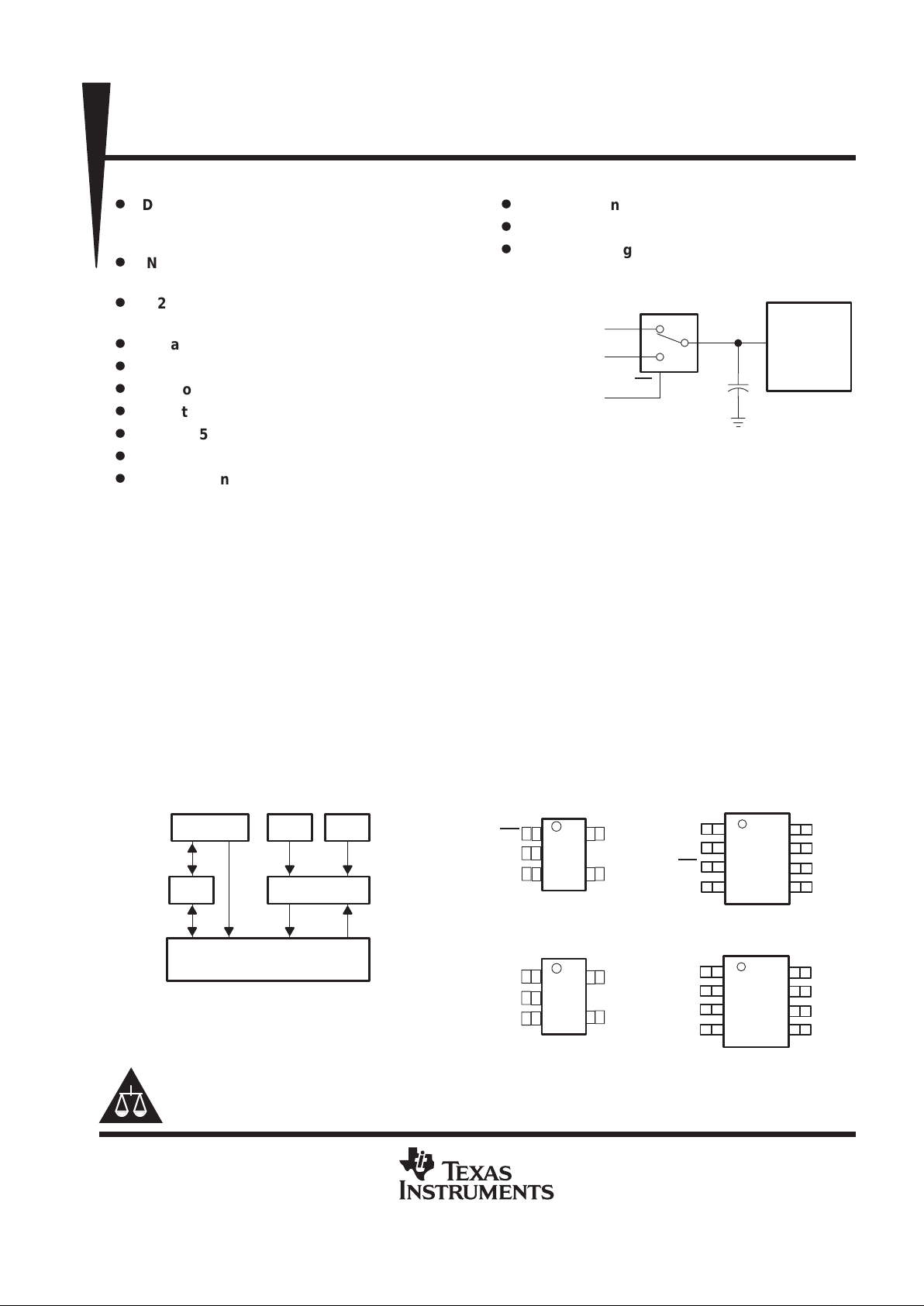
Figure 1. Typical Dual-Input Single-Output
Application
TPS2102
IN1
IN2
EN
3.3 V V
CC
3.3 V V
AUX
D3 or PME Status
Control Signal
Holdup
Capacitor
Controller
(CardBus,
1394,
PCI,
et al.)
3.3 V
TPS2102, TPS2103
V
AUX
POWER-DISTRIBUTION SWITCHES
SLVS234A – SEPTEMBER 1999 – REVISED APRIL 2000
2
POST OFFICE BOX 655303 • DALLAS, TEXAS 75265
Selection Guide, V
AUX
Power-Distribution Switches
DEVICE ENABLE
OPERATING
VOLTAGE RANGE
(V)
MAXIMUM INPUT
CURRENT, IN1
(mA)
MAXIMUM INPUT
CURRENT, IN2
(mA)
AMBIENT
TEMPERATURE RANGE
(°C)
TPS2100 EN 2.7 to 4 500 10 –40 to 70
TPS2101 EN 2.7 to 4 500 10 –40 to 70
TPS2102 EN 2.7 to 4 500 100 –40 to 70
TPS2103 EN 2.7 to 4 500 100 –40 to 70
TPS2104 EN 2.7 to 5.5 500 100 –40 to 85
TPS2105 EN 2.7 to 5.5 500 100 –40 to 85
AVAILABLE OPTIONS FOR TPS2102, TPS2103
PACKAGED DEVICES
T
A
DEVICE ENABLE
SOT-23-5
(DBV)
†
SOIC-8
(D)
°
°
TPS2102 EN TSP2102DBV
†
TPS2102D
–
40°C to 70°C
TPS2103 EN TPS2103DBV
†
TPS2103D
Both packages are available left-end taped and reeled. Add an R suffix to the D device type
(e.g., TPS2103DR).
†
Add T (e.g., TPS2102DBVT) to indicate tape and reel at order quantity of 250 parts.
Add R (e.g., TPS2102DBVR) to indicate tape and reel at order quantity of 3000 parts.
Function Tables
TPS2102 TPS2103
VIN1 VIN2 EN OUT VIN1 VIN2 EN OUT
0 V 0 V XX GND 0 V 0 V XX GND
0 V 3.3 V L GND 0 V 3.3 V H GND
3.3 V 0 V L VIN1 3.3 V 0 V H VIN1
3.3 V 3.3 V L VIN1 3.3 V 3.3 V H VIN1
0 V 3.3 V H VIN2 0 V 3.3 V L VIN2
3.3 V 0 V H VIN2 3.3 V 0 V L VIN2
3.3 V 3.3 V H VIN2 3.3 V 3.3 V L VIN2
XX = don’t care
TPS2102, TPS2103
V
AUX
POWER-DISTRIBUTION SWITCHES
SLVS234A – SEPTEMBER 1999 – REVISED APRIL 2000
3
POST OFFICE BOX 655303 • DALLAS, TEXAS 75265
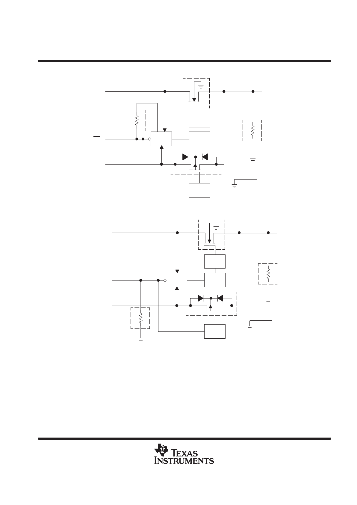
TPS2102 functional block diagram
V
CC
Select
Charge
Pump
Driver
GND
OUT
SW2
1.3 Ω
SW1
250 mΩ
Pullup
Circuit
Driver
IN1
EN
IN2
Discharge
Circuit
TPS2103 functional block diagram
V
CC
Select
Charge
Pump
Driver
GND
OUT
SW2
1.3 Ω
SW1
250 mΩ
Driver
IN1
EN
IN2
Pulldown
Circuit
Discharge
Circuit
TPS2102, TPS2103
V
AUX
POWER-DISTRIBUTION SWITCHES
SLVS234A – SEPTEMBER 1999 – REVISED APRIL 2000
4
POST OFFICE BOX 655303 • DALLAS, TEXAS 75265
Terminal Functions
TERMINAL
NO.
NAME
TPS2102 TPS2103
I/O
DESCRIPTION
DBV D DBV D
EN 1 3 I Active-high enable for IN1-OUT switch
EN 1 3 I Active-low enable for IN1-OUT switch
GND 2 2 2 2 I Ground
IN1
†
5 5 5 5 I Main Input voltage, NMOS drain (250 mΩ), require 0.22 µF bypass
IN2
†
3 1 3 1 I Auxilliary input voltage, PMOS drain (1.3 Ω), require 0.22 µF bypass
OUT 4 7, 8 4 7, 8 O Power switch output
NC 4, 6 4, 6 No connection
†
Unused INx should not be grounded.
detailed description
power switches
n-channel MOSFET
The IN1-OUT n-channel MOSFET power switch has a typical on-resistance of 250 mΩ at 3.3-V input voltage,
and is configured as a high-side switch.
p-channel MOSFET
The IN2-OUT p-channel MOSFET power switch has a typical on-resistance of 1.3 Ω at 3.3-V input voltage and
is configured as a high-side switch. When operating, the p-channel MOSFET quiescent current is reduced to
typically 0.75 µA.
charge pump
An internal charge pump supplies power to the driver circuit and provides the necessary voltage to pull the gate
of the MOSFET above the source. The charge pump operates from input voltages as low as 2.7 V and requires
very little supply current.
driver
The driver controls the gate voltage of the IN1-OUT and IN2-OUT power switches. T o limit large current surges
and reduce the associated electromagnetic interference (EMI) produced, the drivers incorporate circuitry that
controls the rise times and fall times of the output voltage.
enable
The logic enable will turn on the IN2-OUT power switch when a logic high is present on EN (TPS2102) or logic
low is present on EN (TPS2103). A logic low input on EN (TPS2102) or logic high on EN (TPS2103) restores
bias to the drive and control circuits and turns on the IN1-OUT power switch. The enable input is compatible
with both TTL and CMOS logic levels.
the V
AUX
application for CardBus controllers
The PC Card specification requires the support of V
AUX
to the CardBus controller as well as to the PC Card
sockets. Both are 3.3-V requirements; however the CardBus controller’s current demand from the V
AUX
supply
is limited to 10 µA, whereas the PC Card may consume as much as 200 mA. In either implementation, if support
of a wake-up event is required, the controller and the socket will transition from the 3.3-V VCC rail to the 3.3-V
V
AUX
rail when the equipment moves into a low power mode such as D3. The transition from VCC to V
AUX
needs
to be seamless in order to maintain all memory and register information in the system. If V
AUX
is not supported,
the system will lose all register information when it transitions to the D3 state.
TPS2102, TPS2103
V
AUX
POWER-DISTRIBUTION SWITCHES
SLVS234A – SEPTEMBER 1999 – REVISED APRIL 2000
5
POST OFFICE BOX 655303 • DALLAS, TEXAS 75265
absolute maximum ratings over operating free-air temperature (unless otherwise noted)
†
Input voltage range, V
I(IN1)
(see Note 1) –0.3 V to 5 V. . . . . . . . . . . . . . . . . . . . . . . . . . . . . . . . . . . . . . . . . . . . . .
Input voltage range, V
I(IN2)
(see Note 1) –0.3 V to 5 V. . . . . . . . . . . . . . . . . . . . . . . . . . . . . . . . . . . . . . . . . . . . . .
Input voltage range, VI at EN or EN (see Note 1) –0.3 V to 5 V. . . . . . . . . . . . . . . . . . . . . . . . . . . . . . . . . . . . . . .
Output voltage range, VO (see Note 1) –0.3 V to 5 V. . . . . . . . . . . . . . . . . . . . . . . . . . . . . . . . . . . . . . . . . . . . . . .
Continuous output current, I
O(IN1
) 700 mA. . . . . . . . . . . . . . . . . . . . . . . . . . . . . . . . . . . . . . . . . . . . . . . . . . . . . . . .
Continuous output current, I
O(IN2)
140 mA. . . . . . . . . . . . . . . . . . . . . . . . . . . . . . . . . . . . . . . . . . . . . . . . . . . . . . . .
Continuous total power dissipation See dissipation rating table. . . . . . . . . . . . . . . . . . . . . . . . . . . . . . . . . . . . . . .
Operating virtual junction temperature range, TJ –40°C to 85°C. . . . . . . . . . . . . . . . . . . . . . . . . . . . . . . . . . . . . .
Storage temperature range, T
stg
–65°C to 150°C. . . . . . . . . . . . . . . . . . . . . . . . . . . . . . . . . . . . . . . . . . . . . . . . . . .
Lead temperature soldering 1,6 mm (1/16 inch) from case for 10 seconds 260°C. . . . . . . . . . . . . . . . . . . . . . .
Electrostatic discharge (ESD) protection: Human body model 2 kV. . . . . . . . . . . . . . . . . . . . . . . . . . . . . . . . . . .
Machine model 200 V. . . . . . . . . . . . . . . . . . . . . . . . . . . . . . . . . . . . . .
Charged device model 750 V. . . . . . . . . . . . . . . . . . . . . . . . . . . . . . .
†
Stresses beyond those listed under “absolute maximum ratings” may cause permanent damage to the device. These are stress ratings only, and
functional operation of the device at these or any other conditions beyond those indicated under “recommended operating conditions” is not
implied. Exposure to absolute-maximum-rated conditions for extended periods may affect device reliability.
NOTE 1: All voltages are with respect to GND.
DISSIPATION RATING TABLE
PACKAGE
TA < 25°C
POWER RATING
DERATING FACTOR
ABOVE TA = 25°C
TA = 70°C
POWER RATING
TA = 85°C
POWER RATING
DBV 309 mW 3.1 mW/°C 170 mW 123 mW
D 568 mW 5.7 mW/°C 313 mW 227 mW
recommended operating conditions
MIN MAX UNIT
Input voltage, V
I(INx)
2.7 4 V
Input voltage, VI at EN and EN 0 4 V
Continuous output current, I
O(IN1)
500 mA
Continuous output current, I
O(IN2)
100‡mA
Operating virtual junction temperature, T
J
–40 85 °C
‡
The device can deliver up to 220 mA at I
O(IN2)
. However, operation at the higher current levels will result in greater voltage drop across the device,
and greater voltage droop when switching between IN1 and IN2.
electrical characteristics over recommended operating junction temperature range,
V
I(IN1)
= V
(IN2)
= 3.3 V, IO = rated current (unless otherwise noted)
power switch
PARAMETER
TEST
CONDITIONS
†
MIN TYP MAX UNIT
TJ = 25°C 250
IN1-OUT
TJ = 85°C 300 375
mΩ
r
DS(on)
On-state resistance
TJ = 25°C 1.3
IN2-OUT
TJ = 85°C 1.5 2.1
Ω
†
Pulse-testing techniques maintain junction temperature close to ambient termperature; thermal effects must be taken into account separately.
TPS2102, TPS2103
V
AUX
POWER-DISTRIBUTION SWITCHES
SLVS234A – SEPTEMBER 1999 – REVISED APRIL 2000
6
POST OFFICE BOX 655303 • DALLAS, TEXAS 75265
electrical characteristics over recommended operating junction temperature range,
V
I(IN1)
= V
(IN2)
= 3.3 V, IO = rated current (unless otherwise noted) (continued)
enable input (EN and EN)
PARAMETER TEST CONDITIONS MIN TYP MAX UNIT
V
IH
High-level input voltage 2.7 V ≤ V
I(INx)
≤ 4 V 2 V
V
IL
Low-level input voltage 2.7 V ≤ V
I(INx)
≤ 4 V 0.8 V
p
TPS2102 EN = 0 V or EN = V
I(INx)
–0.5 0.5 µA
IIInput current
TPS2103 EN = 0 V or EN = V
I(INx)
–0.5 0.5 µA
supply current
PARAMETER TEST CONDITIONS MIN TYP MAX UNIT
EN = H
,
TJ = 25°C 0.75
EN H,
IN2 selected
–40°C ≤ TJ ≤ 85°C 1.5
µ
A
TPS2102
EN = L
,
TJ = 25°C 14
pp
EN L,
IN1 selected
–40°C ≤ TJ ≤ 85°C 24
µ
A
IISupply current
EN = L,
TJ = 25°C 0.75
,
IN2 selected
–40°C ≤ TJ ≤ 85°C 1.5
µ
A
TPS2103
EN = H,
TJ = 25°C 14
,
IN1 selected
–40°C ≤ TJ ≤ 85°C 24
µ
A
switching characteristics, TJ = 25°C, V
I(IN1)
= V
I(IN2)
= 3.3 V (unless otherwise noted)
†
PARAMETER TEST CONDITIONS
†
MIN TYP MAX UNIT
CL = 1 µF, IL = 500 mA 440
IN1-OUT V
I(IN2)
= 0
CL = 10 µF, IL = 500 mA 440
p
()
CL = 1 µF, IL = 100 mA 370
trOutput rise time
CL = 1 µF, IL = 100 mA 4.6
µ
s
IN2-OUT V
I(IN1)
= 0
CL = 10 µF, IL = 100 mA 50
()
CL = 1 µF, IL = 10 mA 4.6
CL = 1 µF, IL = 500 mA 5
IN1-OUT V
I(IN2)
= 0
CL = 10 µF, IL = 500 mA 100
p
()
CL = 1 µF, IL = 100 mA 13
tfOutput fall time
CL = 1 µF, IL = 100 mA 68
µ
s
IN2-OUT V
I(IN1)
= 0
CL = 10 µF, IL = 100 mA 680
()
CL = 1 µF, IL = 10 mA 720
p
p
IN1-OUT V
I(IN2)
= 0
80
t
PLH
Propagation delay time, low-to-high output
IN2-OUT V
I(IN1)
= 0
C
L
= 10 µF,
I
L
=
100 mA
2
µ
s
p
p
IN1-OUT V
I(IN2)
= 0
3
t
PHL
Propagation delay time, high-to-low output
IN2-OUT V
I(IN1)
= 0
C
L
= 10 µF,
I
L
=
100 mA
40
µ
s
†
All timing parameters refer to Figure 3.

TPS2102, TPS2103
V
AUX
POWER-DISTRIBUTION SWITCHES
SLVS234A – SEPTEMBER 1999 – REVISED APRIL 2000
7
POST OFFICE BOX 655303 • DALLAS, TEXAS 75265
PARAMETER MEASUREMENT INFORMATION
t
PLH
t
PHL
EN or EN
V
O
EN or EN
V
O
50%
10%
V
I
GND
GND
V
I
90%
50%
90%
10%
V
O
GND
V
I
t
r
t
f
Propagation Delay Time, Low-to-High-Level Output Propagation Delay Time, High-to–Low-Level Output
Rise/Fall Time
t
on
t
off
EN or EN
V
O
EN or EN
V
O
50%
10%
V
I
GND
GND
V
I
90%
50%
Turn-on Transition Time
Turn-off Transition Time
WAVEFORMS
OUT
C
L
I
O
LOAD CIRCUIT
Figure 3. Test Circuit and Voltage Waveforms
Table of Timing Diagrams
†
FIGURE
Propagation Delay and Rise Time With 0.1-µF Load, IN1 4
Propagation Delay and Rise Time With 0.1-µF Load, IN2 5
Propagation Delay and Fall Time With 0.1-µF Load, IN1 6
Propagation Delay and Fall Time With 0.1-µF Load, IN2 7
Propagation Delay and Rise Time With 1-µF Load, IN1 8
Propagation Delay and Rise Time With 1-µF Load, IN2 9
Propagation Delay and Fall Time With 1-µF Load, IN1 10
Propagation Delay and Fall Time With 1-µF Load, IN2 11
†
Waveforms shown in Figures 4–11 refer to TPS2102 at TJ = 25°C
TPS2102, TPS2103
V
AUX
POWER-DISTRIBUTION SWITCHES
SLVS234A – SEPTEMBER 1999 – REVISED APRIL 2000
8
POST OFFICE BOX 655303 • DALLAS, TEXAS 75265
PARAMETER MEASUREMENT INFORMATION
Figure 4. Propagation Delay and Rise Time
With 0.1-µF Load, IN1 Turnon
EN
2 V/div)
t – Time – 200 µs/div
V
O
2 V/div)
V
I(IN1)
= 3.3 V
V
I(IN2)
= 0 V
CL = 0.1 µF
RL = 33 Ω
Figure 5. Propagation Delay and Fall Time
With 0.1-µF Load, IN2 Turnon
EN
(2 V/div)
t – Time – 2 µs/div
V
O
(2 V/div)
V
I(IN1)
= 0 V
V
I(IN2)
= 3.3 V
CL = 0.1 µF
RL = 33 Ω
Figure 6. Propagation Delay and Fall Time
With 0.1-µF Load, IN1 Turnoff
EN
(2 V/div)
t – Time – 5 µs/div
V
O
(2 V/div)
V
I(IN1)
= 3.3 V
V
I(IN2)
= 0 V
CL = 0.1 µF
RL = 33 Ω
Figure 7. Propagation Delay and Fall Time
With 0.1-µF Load, IN2 Turnoff
EN
(2 V/div)
t – Time – 5 µs/div
V
O
(2 V/div)
V
I(IN1)
= 0 V
V
I(IN2)
= 3.3 V
CL = 0.1 µF
RL = 33 Ω

TPS2102, TPS2103
V
AUX
POWER-DISTRIBUTION SWITCHES
SLVS234A – SEPTEMBER 1999 – REVISED APRIL 2000
9
POST OFFICE BOX 655303 • DALLAS, TEXAS 75265
PARAMETER MEASUREMENT INFORMATION
EN
(2 V/div)
t – Time – 200 µs/div
V
O
(2 V/div)
V
I(IN1)
= 3.3 V
V
I(IN2)
= 0 V
CL = 1 µF
RL = 33 Ω
Figure 8. Propagation Delay and Rise Time
With 1-µF Load, IN1 Turnon
Figure 9. Propagation Delay and Rise Time
With 1-µF Load, IN2 Turnon
EN
(2 V/div)
t – Time – 2 µs/div
V
O
(2 V/div)
V
I(IN1)
= 0 V
V
I(IN2)
= 3.3 V
CL = 1 µF
RL = 33 Ω
Figure 10. Propagation Delay and Fall Time
With 1-µF Load, IN1 Turnoff
EN
(2 V/div)
t – Time – 10 µs/div
V
O
(2 V/div)
V
I(IN1)
= 3.3 V
V
I(IN2)
= 0 V
CL = 1 µF
RL = 33 Ω
Figure 11. Propagation Delay and Fall Time
With 1-µF Load, IN2 Turnoff
EN
(2 V/div)
t – Time – 50 µs/div
V
O
(2 V/div)
V
I(IN1)
= 0 V
V
I(IN2)
= 3.3 V
CL = 1 µF
RL = 33 Ω

TPS2102, TPS2103
V
AUX
POWER-DISTRIBUTION SWITCHES
SLVS234A – SEPTEMBER 1999 – REVISED APRIL 2000
10
POST OFFICE BOX 655303 • DALLAS, TEXAS 75265
TYPICAL CHARACTERISTICS
Table of Graphs
FIGURE
IN1 Switch Rise Time vs Output Current 12
IN2 Switch Fall Time vs Output Current 13
IN1 Switch Fall Time vs Output Current 14
IN2 Switch Fall Time vs Output Current 15
Output Voltage Droop vs Output Current When Output Is Switched From IN2 to IN1 16
Inrush Current vs Output Capacitance 17
IN1 Supply Current vs Junction Temperature (IN1 Enabled) 18
IN1 Supply Current vs Junction Temperature (IN1 Disabled) 19
IN2 Supply Current vs Junction Temperature (IN2 Enabled) 20
IN2 Supply Current vs Junction Temperature (IN2 Disabled) 21
IN1-OUT On-State Resistance vs Junction Temperature 22
IN2-OUT On-State Resistance vs Junction Temperature 23
Figure 12
380
340
300
0.01 0.1 1 10
– Rise Time –
420
IN1 SWITCH RISE TIME
vs
OUTPUT CURRENT
460
100 1000
CL = 100 µF
CL = 47 µF
CL = 10 µF
CL = 1 µF
CL = 0.1 µF
IO – Output Current – mA
t
r
sµ
V
I(IN1)
= 3.3 V
V
I(IN2)
= 0 V
TJ = 25°C
Figure 13
10
1
0.1
0 102030405060
100
IN2 SWITCH RISE TIME
vs
OUTPUT CURRENT
1000
70 80 90 100
– Rise Time –
CL = 100 µF
CL = 47 µF
CL = 10 µF
CL = 1 µF
CL = 0.1 µF
IO – Output Current – mA
t
r
sµ
V
I(IN1)
= 0 V
V
I(IN2)
= 3.3 V
TJ = 25°C

TPS2102, TPS2103
V
AUX
POWER-DISTRIBUTION SWITCHES
SLVS234A – SEPTEMBER 1999 – REVISED APRIL 2000
11
POST OFFICE BOX 655303 • DALLAS, TEXAS 75265
TYPICAL CHARACTERISTICS
Figure 14
100
10
0.1
0.01 0.1 1 10
1000
IN1 SWITCH FALL TIME
vs
OUTPUT CURRENT
10000
100 1000
– Fall Time –
CL = 100 µF
CL = 47 µF
CL = 10 µF
CL = 1 µF
CL = 0.1 µF
IO – Output Current – mA
t
f
sµ
V
I(IN1)
= 3.3 V
V
I(IN2)
= 0 V
TJ = 25°C
1
Figure 15
10
1
0.001
0.01 0.1
100
IN2 SWITCH FALL TIME
vs
OUTPUT CURRENT
1000
1 100
– Output Fall Time – ms
CL = 100 µF
CL = 10 µF
CL = 1 µF
CL = 0.1 µF
IO – Output Current – mA
t
f
V
I(IN1)
= 0 V
V
I(IN2)
= 3.3 V
TJ = 25°C
CL = 47 µF
10
0.1
0.01
Figure 16
0.4
0.2
0
0.01 0.1
0.6
0.8
1
1 100
– Output Voltage Droop – V
OUTPUT VOLTAGE DROOP
vs
OUTPUT CURRENT WHEN OUTPUT
IS SWITCHED FROM IN2 TO IN1
†
V
O
CL = 100 µF
CL = 10 µF
CL = 1 µF
CL = 0.1 µF
IO – Output Current – mA
V
I(IN1)
= 3.3 V
V
I(IN2)
= 3.3 V
TJ = 25°C
CL = 47 µF
10
CL = 220 µF
Figure 17
1
0
0 100 200 300
Inrush Current – A
1.5
2
INRUSH CURRENT
vs
OUTPUT CAPACITANCE
2.5
400 500
0.5
Co – Output Capacitance – µF
V
I(IN1)
= 3.3 V
V
I(IN2)
= 0 V
RL = 6.6 Ω
TJ = 25°C
†
If switching from IN1 to IN2, the voltage droop is much smaller. Therefore, the load capacitance should be chosen according to the curves in
Figure 16.
TPS2102, TPS2103
V
AUX
POWER-DISTRIBUTION SWITCHES
SLVS234A – SEPTEMBER 1999 – REVISED APRIL 2000
12
POST OFFICE BOX 655303 • DALLAS, TEXAS 75265
TYPICAL CHARACTERISTICS
Figure 18
– Supply Current –I
CC
Aµ
15
13
9
–40 –10 20 50
17
IN1 SUPPLY CURRENT
vs
JUNCTION TEMPERATURE (IN1 ENABLED)
21
11080
V
I(IN1)
= 4 V
TJ – Junction Temperature – °C
19
V
I(IN1)
= 3.3 V
11
V
I(IN1)
= 2.7 V
Figure 19
– Supply Current –I
CC
Aµ
0.25
–40 –10 20 50
IN1 SUPPLY CURRENT
vs
JUNCTION TEMPERATURE (IN1 DISABLED)
0.35
11
0
80
V
I(IN1)
= 4 V
TJ – Junction Temperature – °C
V
I(IN1)
= 2.7 V
0.33
0.31
0.29
0.27
V
I(IN1)
= 3.3 V
– Supply Current –I
CC
Aµ
0.35
–40 –10 20 50
IN2 SUPPLY CURRENT
vs
JUNCTION TEMPERATURE (IN2 ENABLED)
0.59
11080
V
I(IN2)
= 4 V
TJ – Junction Temperature – °C
V
I(IN2)
= 2.7 V
0.53
0.47
0.41
V
I(IN2)
= 3.3 V
Figure 20
Figure 21
– Supply Current –I
CC
Aµ
0.15
–40 –10 20 50
IN2 SUPPLY CURRENT
vs
JUNCTION TEMPERATURE (IN2 DISABLED)
0.25
11
0
80
V
I(IN2)
= 4 V
TJ – Junction Temperature – °C
V
I(IN2)
= 2.7 V
0.23
0.21
0.19
0.17
V
I(IN2)
= 3.3 V
TPS2102, TPS2103
V
AUX
POWER-DISTRIBUTION SWITCHES
SLVS234A – SEPTEMBER 1999 – REVISED APRIL 2000
13
POST OFFICE BOX 655303 • DALLAS, TEXAS 75265
TYPICAL CHARACTERISTICS
Figure 22
280
240
200
–40 –10 20 50
– IN1-OUT On-State Resistance –
320
IN1-OUT ON-STATE RESISTANCE
vs
JUNCTION TEMPERATURE
360
80 110
r
on
mΩ
V
I(IN1)
= 4 V
V
I(IN1)
= 3.3 V
V
I(IN1)
= 2.7 V
TJ – Junction Temperature – °C
Figure 23
2
1.5
1
0.5
–40 –10 20 50
IN2-OUT ON-STATE RESISTANCE
vs
JUNCTION TEMPERATURE
2.5
80 110
V
I(IN2)
= 4 V
V
I(IN2)
= 3.3 V
V
I(IN2)
= 2.7 V
TJ – Junction Temperature – °C
– IN1-OUT On-State Resistance –
r
on
mΩ
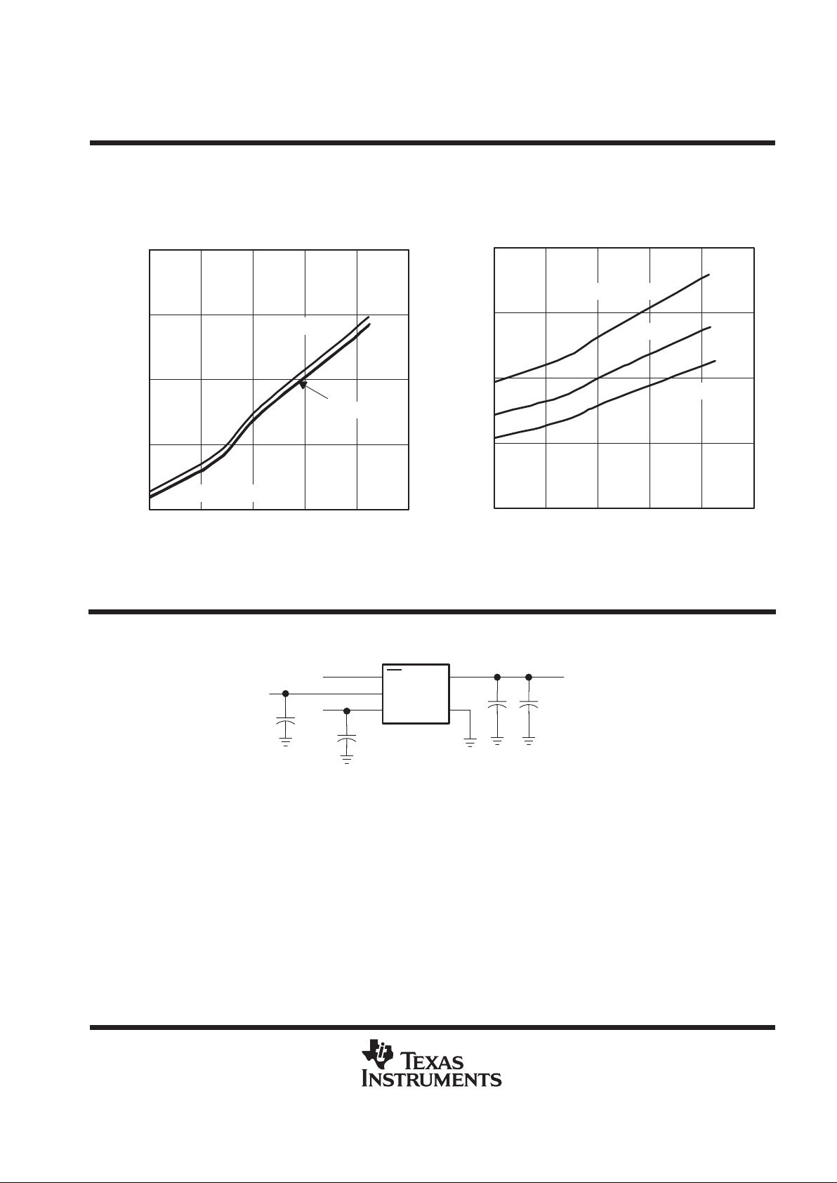
APPLICATION INFORMATION
EN
IN1
IN2
OUT
GND
3.3 V V
AUX
3.3 V V
CC
CardBus or System Controller
TPS2102
0.22 µF
0.22 µF
0.1 µF xx µF
3.3 V
Figure 24. Typical Application
power-supply considerations
A 0.22-µF ceramic bypass capacitor between IN and GND, close to the device is recommended. The output
capacitor should be chosen based on the size of the load during the transition of the switch. A 220-µF capacitor
is recommended for 100 mA loads. Typical output capacitors (xx µF, shown in Figure 24) required for a given
load can be determined from Figure 16 which shows the output voltage droop when output is switched from IN2
to IN1. The output voltage droop is insignificant when output is switched from IN1 to IN2. Additionally , bypassing
the output with a 0.1-µF ceramic capacitor improves the immunity of the device to short-circuit transients.

TPS2102, TPS2103
V
AUX
POWER-DISTRIBUTION SWITCHES
SLVS234A – SEPTEMBER 1999 – REVISED APRIL 2000
14
POST OFFICE BOX 655303 • DALLAS, TEXAS 75265
APPLICATION INFORMATION
power supply considerations (continued)
switch transition
The n-channel MOSFET on IN1 uses a charge pump to create the gate-drive voltage, which gives the IN1 switch
a rise time of approximately 0.5 ms. The p-channel MOSFET on IN2 has a simpler drive circuit that allows a
rise time of approximately 5 µs. Because the device has two switches and a single enable pin, these rise times
are seen as transition times, from IN1 to IN2, or IN2 to IN1, by the output. The controlled transition times help
limit the surge currents seen by the power supply during switching.
thermal protection
Thermal protection provided on the IN1 switch prevents damage to the IC when heavy-overload or short-circuit
faults are present for extended periods of time. The increased dissipation causes the junction temperature to
rise to dangerously high levels. The protection circuit senses the junction temperature of the switch and shuts
it off at approximately 145°C (TJ). The switch remains off until the junction temperature has dropped
approximately 10°C. The switch continues to cycle in this manner until the load fault or input power is removed.
undervoltage lockout
An undervoltage lockout function is provided to ensure that the power switch is in the off state at power-up.
Whenever the input voltage falls below approximately 2 V, the power switch quickly turns off. This function
facilitates the design of hot-insertion systems that may not have the capability to turn off the power switch before
input power is removed. Upon reinsertion, the power switch will be turned on with a controlled rise time to reduce
EMI and voltage overshoots.
power dissipation and junction temperature
The low on-resistance on the n-channel MOSFET allows small surface-mount packages, such as SOIC, to pass
large currents. The thermal resistances of these packages are high compared to that of power packages; it is
good design practice to check power dissipation and junction temperature. First, find ron at the input voltage,
and operating temperature. As an initial estimate, use the highest operating ambient temperature of interest and
read ron from Figure 22 or Figure 23. Next calculate the power dissipation using:
PD+
ron
I
2
Finally, calculate the junction temperature:
TJ+
PD
R
q
JA
)
T
A
Where:
T
A
= Ambient temperature
R
θJA
= Thermal resistance
Compare the calculated junction temperature with the initial estimate. If they do not agree within a few degrees,
repeat the calculation using the calculated value as the new estimate. Two or three iterations are generally
sufficient to obtain a reasonable answer.
ESD protection
All TPS2102 and TPS2103 terminals incorporate ESD-protection circuitry designed to withstand a 2-kV
human-body-model, 750-V CDM, and 200-V machine-model discharge as defined in MIL-STD-883C.

TPS2102, TPS2103
V
AUX
POWER-DISTRIBUTION SWITCHES
SLVS234A – SEPTEMBER 1999 – REVISED APRIL 2000
15
POST OFFICE BOX 655303 • DALLAS, TEXAS 75265
MECHANICAL DATA
DBV (R-PDSO-G5) PLASTIC SMALL-OUTLINE
0,10
M
0,20
0,95
0°–8°
0,25
0,35
0,55
Gage Plane
0,15 NOM
4073253-4/E 05/99
2,60
3,00
0,50
0,30
1,50
1,70
45
31
2,80
3,00
0,95
1,45
0,05 MIN
Seating Plane
NOTES: A. All linear dimensions are in millimeters.
B. This drawing is subject to change without notice.
C. Body dimensions do not include mold flash or protrusion.
D. Falls within JEDEC MO-178

TPS2102, TPS2103
V
AUX
POWER-DISTRIBUTION SWITCHES
SLVS234A – SEPTEMBER 1999 – REVISED APRIL 2000
16
POST OFFICE BOX 655303 • DALLAS, TEXAS 75265
MECHANICAL DATA
D (R-PDSO-G**) PLASTIC SMALL-OUTLINE PACKAGE
14 PINS SHOWN
4040047/D 10/96
0.228 (5,80)
0.244 (6,20)
0.069 (1,75) MAX
0.010 (0,25)
0.004 (0,10)
1
14
0.014 (0,35)
0.020 (0,51)
A
0.157 (4,00)
0.150 (3,81)
7
8
0.044 (1,12)
0.016 (0,40)
Seating Plane
0.010 (0,25)
PINS **
0.008 (0,20) NOM
A MIN
A MAX
DIM
Gage Plane
0.189
(4,80)
(5,00)
0.197
8
(8,55)
(8,75)
0.337
14
0.344
(9,80)
16
0.394
(10,00)
0.386
0.004 (0,10)
M
0.010 (0,25)
0.050 (1,27)
0°–8°
NOTES: A. All linear dimensions are in inches (millimeters).
B. This drawing is subject to change without notice.
C. Body dimensions do not include mold flash or protrusion, not to exceed 0.006 (0,15).
D. Falls within JEDEC MS-012

IMPORTANT NOTICE
T exas Instruments and its subsidiaries (TI) reserve the right to make changes to their products or to discontinue
any product or service without notice, and advise customers to obtain the latest version of relevant information
to verify, before placing orders, that information being relied on is current and complete. All products are sold
subject to the terms and conditions of sale supplied at the time of order acknowledgment, including those
pertaining to warranty, patent infringement, and limitation of liability.
TI warrants performance of its semiconductor products to the specifications applicable at the time of sale in
accordance with TI’s standard warranty. Testing and other quality control techniques are utilized to the extent
TI deems necessary to support this warranty. Specific testing of all parameters of each device is not necessarily
performed, except those mandated by government requirements.
Customers are responsible for their applications using TI components.
In order to minimize risks associated with the customer’s applications, adequate design and operating
safeguards must be provided by the customer to minimize inherent or procedural hazards.
TI assumes no liability for applications assistance or customer product design. TI does not warrant or represent
that any license, either express or implied, is granted under any patent right, copyright, mask work right, or other
intellectual property right of TI covering or relating to any combination, machine, or process in which such
semiconductor products or services might be or are used. TI’s publication of information regarding any third
party’s products or services does not constitute TI’s approval, warranty or endorsement thereof.
Copyright 2000, Texas Instruments Incorporated
 Loading...