

1
2
3
4
5
6
OUT2
OC1
OUT 1
EN1
GND
IN
TPS2062A/TPS2066A
DPACKAGE
(TOP VIEW)
7
8
EN2 OC2
5
6
TPS2062A/TPS2066A
DRBPACKAGE
(TOP VIEW)
7
8
PAD
1
2
3
4
EN1
GND
IN
EN2
OUT2
OC1
OUT1
OC2
Enableinputsareactivelowforall TPS2062A
andactivehighforall TPS2066A
TPS2014600mA
TPS20151 A
TPS2041B500mA
TPS2051B500mA
TPS2045A 250mA
TPS2049100mA
TPS2055A 250mA
TPS20611 A
TPS20651 A
TPS20681.5 A
TPS20691.5 A
TPS201xA 0.2 A -2A
TPS202x0.2 A -2A
TPS203x0.2 A -2A
www.ti.com
........................................................................................................................................... SLVS798F – JANUARY 2008 – REVISED NOVEMBER 2008
TWO CHANNEL, CURRENT-LIMITED, POWER-DISTRIBUTION SWITCHES
1
FEATURES APPLICATIONS
2
• 70-m Ω High-Side MOSFET
• 1-A Continuous Current
• Thermal and Short-Circuit Protection
• Accurate Current-Limit
(1.2 A min, 2 A max)
• Operating Range: 2.7 V to 5.5 V
• 0.6-ms Typical Rise Time
• Undervoltage Lockout
• Deglitched Fault Report ( OCx)
• No OCx Glitch During Power Up
• 1- µ A Maximum Standby Supply Current
• Bidirectional Switch
• Ambient Temperature Range: – 40 ° C to 85 ° C
• Built-in Soft-Start
• UL Listed -- File No. E169910, Both Single and
Ganged Channel Configuration
TPS2062A
TPS2066A
• Heavy Capacitive Loads
• Short-Circuit Protection
DESCRIPTION
The TPS206xA power-distribution switches are intended for applications where heavy capacitive loads and
short-circuits are likely to be encountered. The TPS206xA family is pin-for-pin compatible with the TPS206x
family with a tighter overcurrent tolerance. This family of devices incorporates two 70-m Ω N-channel MOSFET
power switches for power-distribution systems that require multiple power switches in a single package. Each
switch is controlled by a logic enable input. Gate drive is provided by an internal charge pump designed to
control the power-switch rise and fall times to minimize current surges during switching. The charge pump
requires no external components and allows operation from supplies as low as 2.7 V.
Each device limits the output current to a safe level by switching into a constant-current mode when the output
load exceeds the current-limit threshold or a short is present. Individual channels indicate the presence of an
overcurrent condition by asserting its corresponding OCx output (active low). Thermal protection circuitry
disables the device during overcurrent or short-circuit events to prevent permanent damage. The device recovers
from thermal shutdown automatically once the device has cooled sufficiently. The device provides undervoltage
lockout to disable the device until the input voltage rises above 2.0 V. The TPS206xA is designed to current limit
at 1.6 A typically per channel.
1
2 PowerPAD is a trademark of Texas Instruments.
PRODUCTION DATA information is current as of publication date.
Products conform to specifications per the terms of the Texas
Instruments standard warranty. Production processing does not
necessarily include testing of all parameters.
Please be aware that an important notice concerning availability, standard warranty, and use in critical applications of Texas Instruments semiconductor products and disclaimers thereto appears at the end of this data sheet.
Copyright © 2008, Texas Instruments Incorporated
TPS2062A
TPS2066A
SLVS798F – JANUARY 2008 – REVISED NOVEMBER 2008 ...........................................................................................................................................
This device contains circuits to protect its inputs and outputs against damage due to high static voltages or electrostatic fields.
These circuits have been qualified to protect this device against electrostatic discharges (ESD) of up to 2 kV according to
MIL-STD-883C, Method 3015; however, it is advised that precautions be taken to avoid application of any voltage higher than
maximum-rated voltages to these high-impedance circuits. During storage or handling the device leads should be shorted together
or the device should be placed in conductive foam. In a circuit, unused inputs should always be connected to an appropriate logic
voltage level, preferably either VCC or ground. Specific guidelines for handling devices of this type are contained in the publication
Guidelines for Handling Electrostatic-Discharge-Sensitive (ESDS) Devices and Assemblies available from Texas Instruments.
AVAILABLE OPTION AND ORDERING INFORMATION
PACKAGE
– 40 ° C to
85 ° C
RECOMMENDED
T
ENABLE SHORT-CIRCUIT
A
MAXIMUM D-8 DRB-8
CONTINUOUS LOAD (SOIC) (SON)
CURRENT
Active
low
Active
1 A 1.6 A
high
TYPICAL
LIMIT
PART # STATUS PART # STATUS
TPS2062AD AVAILABLE TPS2062ADRB AVAILABLE
TPS2066AD AVAILABLE TPS2066ADRB AVAILABLE
(1) For the most current package and ordering information, see the Package Option Addendum at the end of this document, or see the TI
website at www.ti.com .
(1)
www.ti.com
ABSOLUTE MAXIMUM RATINGS
over operating temperature range unless otherwise noted
V
Input voltage range IN – 0.3 to 6 V
I
V
Output voltage range OUTx – 0.3 to 6 V
O
Input voltage range ENx, ENx – 0.3 to 6 V
V
I
Voltage range OCx – 0.3 to 6 V
I
Continuous output current OUTx Internally limited
O
Continuous total power dissipation See " Dissipation Rating Table "
T
Operating junction temperature range – 40 to 125 ° C
J
T
Storage temperature range – 65 to 150 ° C
stg
Electrostatic discharge
ESD
protection
(1) Stresses beyond those listed under absolute maximum ratings may cause permanent damage to the device. These are stress ratings
only, and functional operation of the device at these or any other conditions beyond those indicated under recommended operating
conditions is not implied. Exposure to absolute-maximum-rated conditions for extended periods may affect device reliability.
(2) All voltages are with respect to GND.
Human body model MIL-STD-883C 2 kV
Charge device model (CDM) 500 V
(1) (2)
VALUE UNIT
DISSIPATION RATING TABLE
BOARD PACKAGE
(1)
Low-K
(2)
High-K
(3)
Low-K
(5)
High-K
D-8 170 ° C/W 586 mW 5.86 mW/ ° C 320 mW 234 mW
D-8 97.5 ° C/W 1025 mW 10.26 mW/ ° C 564 mW 410 mW
(4)
DRB
(4)
DRB
THERMAL POWER FACTOR POWER POWER
RESISTANCE θ
JA
270 ° C/W 370 mW 3.71 mW/ ° C 203 mW 148 mW
60 ° C/W 1600 mW 16.67 mW/ ° C 916 mW 666 mW
(1) The JEDEC low-K (1s) board used to dervie this data was a 3in x 3in, two-layer board with 2-ounce copper traces on top of the board.
(2) The JEDEC high-K (2s2p) board used to dervive this data was a 3in x 3in, multilayer board with 1-ounce internal power and ground
planes and 2-ounce copper traces on top and bottom of the board.
(3) Soldered PowerPAD on a standard 2-layer PCB without vias for thermal pad. See TI application note SLMA002 for further details.
(4) See Recommended Operating Conditions Table for PowePad connection guidelines to meet qualifying conditions for CB Certificate
(5) Soldered PowerPAD on a standard 4-layer PCB with vias for thermal pad. See TI application note SLMA002 for further details.
TA≤ 25 ° C DERATING TA= 70 ° C TA= 85 ° C
RATING ABOVE TA= RATING RATING
25 ° C
2 Submit Documentation Feedback Copyright © 2008, Texas Instruments Incorporated
Product Folder Link(s): TPS2062A TPS2066A
TPS2062A
TPS2066A
www.ti.com
........................................................................................................................................... SLVS798F – JANUARY 2008 – REVISED NOVEMBER 2008
RECOMMENDED OPERATING CONDITIONS
(1)
MIN MAX UNIT
V
I
I
O
T
J
Input voltage, IN 2.7 5.5 V
Input voltage, ENx, ENx 0 5.5 V
Continuous output current, OUTx 0 1 A
Operating virtual junction temperature – 40 125 ° C
(1) The PowePad must be connected externally to GND pin to meet qualifying conditions for CB Certificate (DRB package only)
ELECTRICAL CHARACTERISTICS
over recommended operating junction temperature range, VI= 5.5 V, IO= 1 A, V
(unless otherwise noted)
PARAMETER TEST CONDITIONS
POWER SWITCH
r
DS(on)
t
r
t
f
ENABLE INPUT EN OR EN
V
IH
V
IL
I
I
t
on
t
off
CURRENT LIMIT
I
OS
I
OC
I
OS_G
I
OC_G
SUPPLY CURRENT
I
IL
I
IH
I
lkg
Reverse leakage current VO= 5.5 V, VI= 0 V TJ= 25 ° C 0.2 µ A
UNDERVOLTAGE LOCKOUT
OVERCURRENT FLAG
V
OL
THERMAL SHUTDOWN
Thermal shutdown threshold 135 ° C
Recovery from thermal shutdown 125 ° C
Hysteresis 10 ° C
(1) Pulsed load testing used to maintain junction temperature close to ambient
(2) The thermal shutdown only reacts under overcurrent conditions.
Static drain-source on-state resistance 2.7 V ≤ VI≤ 5.5 V, IO= 1 A m Ω
Rise time, output
Fall time, output
High-level input voltage 2
Low-level input voltage 0.8
VI= 5.5 V 0.6 1.5
VI= 2.7 V 0.4 1
VI= 5.5 V 0.05 0.5
CL= 1 µ F,
RL= 5 Ω , TJ= 25 ° C
VI= 2.7 V 0.05 0.5
2.7 V ≤ VI≤ 5.5 V V
Input current -0.5 0.5 µ A
Turnon time 3
Turnoff time 3
CL= 100 µ F, RL= 5 Ω ms
Short-circuit output current per VI= 5 V, OUTx connected to GND,
channel device enabled into short-circuit
Overcurrent trip threshold VIN= 5 V I
Ganged short-circuit output current
VI= 5 V, OUT1 & OUT2 connected to
GND, device enabled into short-circuit
Ganged overcurrent trip threshold VI= 5 V, OUT1 & OUT2 tied together I
Supply current, device disabled No load on OUT µ A
Supply current, device enabled No load on OUT µ A
Leakage current, device disabled OUT connected to ground – 40 ° C ≤ TJ≤ 125 ° C 1 µ A
Low-level input voltage, IN VIrising 2 2.5 V
Hysteresis, IN VIfalling 75 mV
Output low voltage, OC I
Off-state current V
= 5 mA 0.4 V
/OCx
= 5.0 V or 3.3 V 1 µ A
/OCx
OC deglitch OCx assertion or de-assertion 4 8 15 ms
(2)
= 0 V (TPS2062A) or V
/ENx
(1)
MIN TYP MAX UNIT
= 5.5 V
ENx
TJ= 25 ° C 70 100
– 40 ° C ≤ TJ≤ 125 ° C 135
TJ= 25 ° C 1.2 1.6 2.0
– 40 ° C ≤ TJ≤ 125 ° C 1.1 1.6 2.1
2.1 2.45 A
OS
TJ= 25 ° C 2.4 3.2 4.0
– 40 ° C ≤ TJ≤ 125 ° C 2.2 3.2 4.2 A
4.2 4.9
OS_G
TJ= 25 ° C 0.5 1
– 40 ° C ≤ TJ≤ 125 ° C 0.5 5
TJ= 25 ° C 50 60
– 40 ° C ≤ TJ≤ 125 ° C 50 75
ms
A
Copyright © 2008, Texas Instruments Incorporated Submit Documentation Feedback 3
Product Folder Link(s): TPS2062A TPS2066A
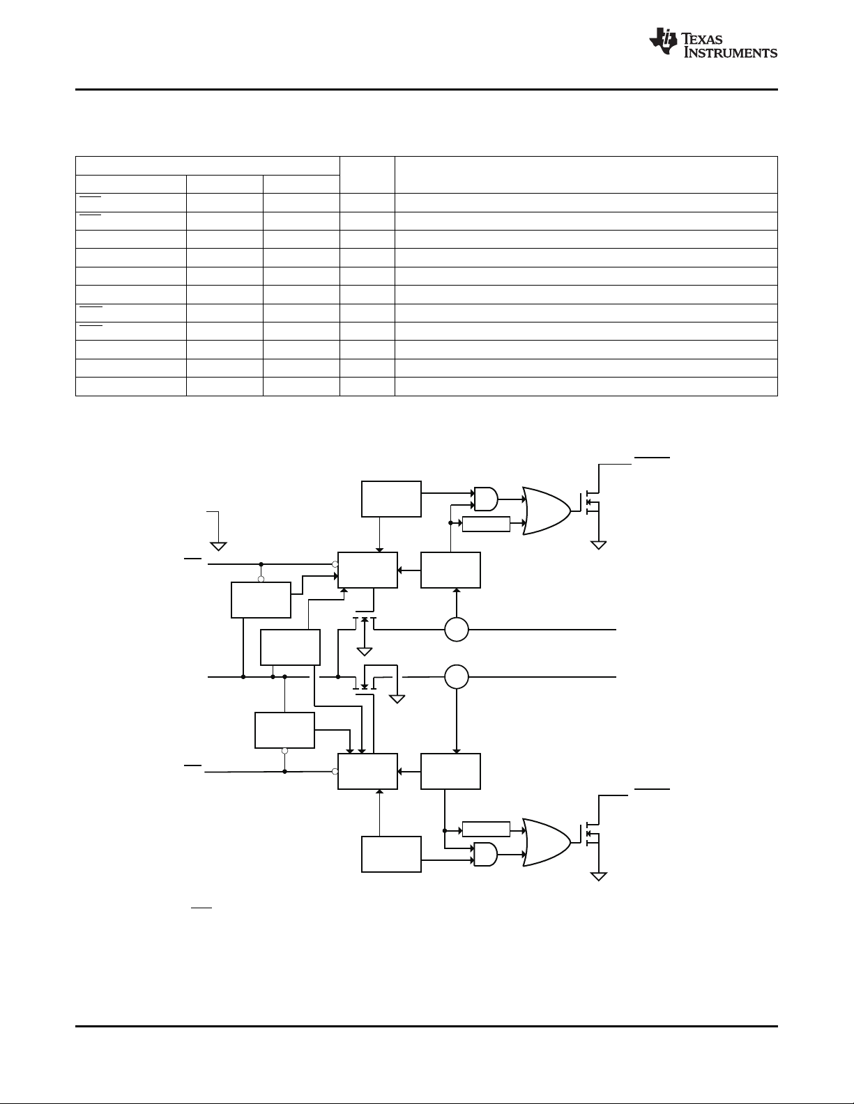
Charge
Pump
Driver
Current
Limit
Thermal
Sense
Deglitch
IN
GND
EN2
OUT2
FAULT 2
CS
Current
Sense
CS
Driver
Current
Limit
UVLO
Charge
Pump
Thermal
Sense
Deglitch
FAULT 1
OUT1
EN1
TPS2062A
TPS2066A
SLVS798F – JANUARY 2008 – REVISED NOVEMBER 2008 ...........................................................................................................................................
DEVICE INFORMATION
Terminal Functions
TERMINAL
NAME TPS2062A TPS2066A
EN1 3 — I Enable input, logic low turns on power switch IN-OUT1
EN2 4 — I Enable input, logic low turns on power switch IN-OUT2
EN1 — 3 I Enable input, logic high turns on power switch IN-OUT1
EN2 — 4 I Enable input, logic high turns on power switch IN-OUT2
GND 1 1 Ground
IN 2 2 I Input voltage
OC1 8 8 O Channel 1 over-current indicator; the output is open-drain, active low type
OC2 5 5 O Channel 2 over-current indicator; the output is open-drain, active low type
OUT1 7 7 O Power-switch output, IN-OUT1
OUT2 6 6 O Power-switch output, IN-OUT2
PowerPAD™
(1)
PAD PAD Connect PowerPAD to GND for proper operation (DRB package only)
(1) See the Recommended Operating Conditions Table for PowePad connection guidelines to meet qualifying conditions for CB Certificate.
I/O DESCRIPTION
FUNCTIONAL BLOCK DIAGRAM
www.ti.com
A. Current sense
B. Active low ( ENx) for TPS2062A. Active high (ENx) for TPS2066A.
4 Submit Documentation Feedback Copyright © 2008, Texas Instruments Incorporated
Product Folder Link(s): TPS2062A TPS2066A
R
L
C
L
OUT
TEST CIRCUIT
t
r
t
f
10%
90%
10%
90%
V
OUT
t
on
t
off
10%
90%
50%50%
V
EN
V
OUT
V
EN
V
OUT
t
on
t
off
50%
50%
10%
90%
VOLTAGEWAVEFORMS
V
I(EN)
5V/div
V
O(OUT)
2V/div
RL=5W ,
CL=1 mF
T
A
=25°C
t − Time − 500 ms/div
V
I(EN)
5V/div
V
O(OUT)
2V/div
t − Time − 500 ms/div
R =5 ,
C =1 F,
T =25°C
L
L
A
W
m
TPS2062A
TPS2066A
www.ti.com
........................................................................................................................................... SLVS798F – JANUARY 2008 – REVISED NOVEMBER 2008
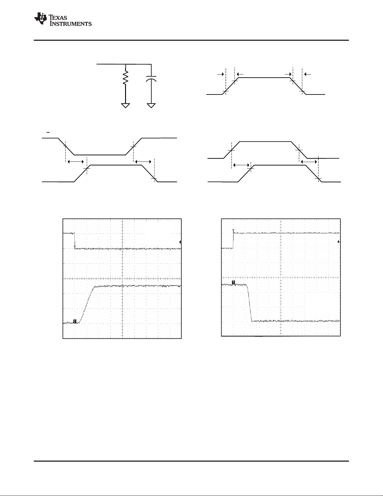
PARAMETER MEASUREMENT INFORMATION
Figure 1. Test Circuit and Voltage Waveforms
Figure 2. Turnon Delay and Rise Time With 1- µ F Load Figure 3. Turnoff Delay and Fall Time With 1- µ F Load
Copyright © 2008, Texas Instruments Incorporated Submit Documentation Feedback 5
Product Folder Link(s): TPS2062A TPS2066A
V
I(EN)
5V/div
V
O(OUT)
2V/div
t − Time − 500 ms/div
R =5 ,
C =100 F,
T =25°C
L
L
A
W
m
V
O(OUT)
2V/div
V
I(EN)
5V/div
t − Time − 500 ms/div
R =5 ,
C =100 F,
T =25°C
L
L
A
W
m
V
I(EN)
5V/div
I
O(OUT)
500mA/div
t − Time − 500 ms/div
V
I(EN)
5V/div
I
O(OUT)
500mA/div
470 mF
100 mF
220 mF
VIN=5V,
RL=5W ,
T
A
=25°C
t − Time − 1ms/div
TPS2062A
TPS2066A
SLVS798F – JANUARY 2008 – REVISED NOVEMBER 2008 ...........................................................................................................................................
PARAMETER MEASUREMENT INFORMATION (continued)
Figure 4. Turnon Delay and Rise Time With 100- µ F Load Figure 5. Turnoff Delay and Fall Time With 100- µ F Load
www.ti.com
Figure 6. Short-Circuit Current, Figure 7. Inrush Current With Different
Device Enabled Into Short Load Capacitance
6 Submit Documentation Feedback Copyright © 2008, Texas Instruments Incorporated
Product Folder Link(s): TPS2062A TPS2066A
V
O(OC)
2V/div
I
O(OUT)
1A/div
t − Time − 2ms/div
V
O(OC)
2V/div
I
O(OUT)
1A/div
t − Time − 2ms/div
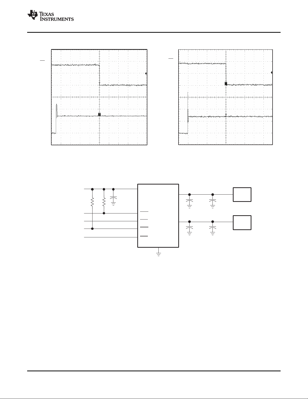
IN
OC1
EN1
OC2
2
8
5
7
0.1 Fm 22 Fm
0.1 Fm 22 Fm
Load
Load
OUT1
OUT2
PowerSupply
2.7Vto5.5V
6
EN2
3
4
GND
0.1 Fm
TPS2062A
1
TPS2062A
TPS2066A
www.ti.com
........................................................................................................................................... SLVS798F – JANUARY 2008 – REVISED NOVEMBER 2008
PARAMETER MEASUREMENT INFORMATION (continued)
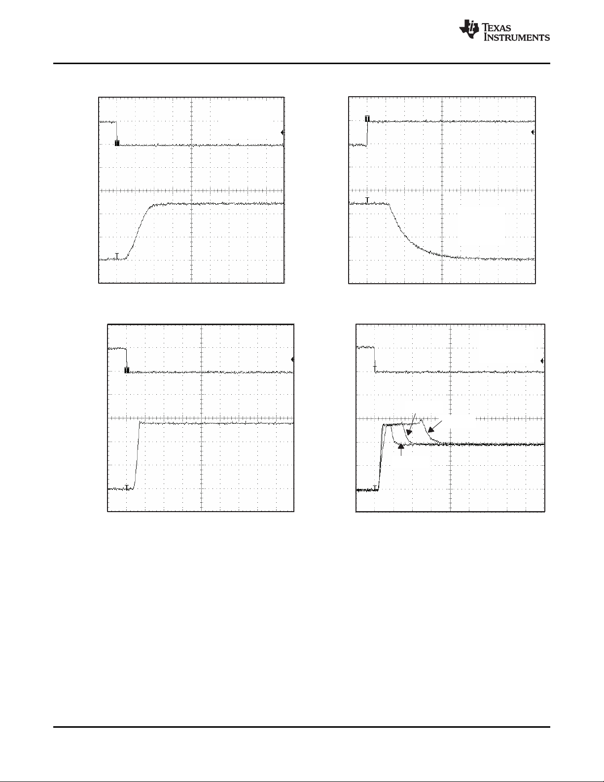
Figure 8. 2- Ω Load Connected to Enabled Device Figure 9. 1- Ω Load Connected to Enabled Device
POWER-SUPPLY CONSIDERATIONS
Figure 10. Typical Application
DETAILED DESCRIPTION
OVERVIEW
The devices are current-limited, power distribution switches using N-channel MOSFETs for applications where
short-circuits or heavy capacitive loads will be encountered. These devices have a minimum fixed current-limit
threshold above 1.1 A allowing for continuous operation up to 1 A per channel. Overtemperature protection is an
addtional device shutdown feature. Each device incorporates an internal charge pump and gate drive circuitry
necessary to drive the N-channel MOSFETs. The charge pump supplies power to the driver circuit and provides
the necessary voltage to pull the gate of the MOSFET above the source. The charge pump operates from input
voltages as low as 2.7 V and requires little supply current. The driver controls the gate voltage of the power
switch. The driver incorporates circuitry that controls the rise and fall times of the output voltage to provide
"soft-start" and to limit large current and voltage surges.
Copyright © 2008, Texas Instruments Incorporated Submit Documentation Feedback 7
Product Folder Link(s): TPS2062A TPS2066A

TPS2062A
TPS2066A
SLVS798F – JANUARY 2008 – REVISED NOVEMBER 2008 ...........................................................................................................................................
OVERCURRENT
When an overcurrent condition is detected, the device maintains a constant output current and reduces the
output voltage accordingly. Three possible overload conditions can occur.
In the first condition, the output has been shorted before the device is enabled or before voltage is applied to IN.
The device senses the short and immediately switches into a constant-current output. In the second condition, a
short or an overload occurs while the device is enabled. At the instant the overload occurs, high currents may
flow for several microseconds before the current-limit circuit can react. The device operates in constant-current
mode after the current-limit circuit has responded. In the third condition, the load is increased gradually beyond
the recommended operating current. The current is permitted to rise until the current-limit threshold is reached.
The devices are capable of delivering current up to the current-limit threshold without damage. Once the
threshold is reached, the device switches into constant-current mode.
Complete shutdown occurs only if the fault is present long enough to activate thermal limiting. The device will
remain off until the junction temperature cools approximately 10 ° C and will then re-start. The device will continue
to cycle on/off until the overcurrent condition is removed.
OCx RESPONSE
Each OCx open-drain output is asserted (active low) during an overcurrent or overtemperature condition on that
channel. The output remains asserted until the fault condition is removed. The TPS206xA eliminates false OCx
reporting by using internal delay circuitry after entering or leaving an overcurrent condition. This "deglitch" time is
approximately 8-ms. This ensures that OCx is not accidentally asserted due to normal operation such as starting
into a heavy capacitive load. Overtemperature conditions are not deglitched and assert and de-assert the OCx
signal immediately.
www.ti.com
UNDERVOLTAGE LOCKOUT (UVLO)
The undervoltage lockout (UVLO) circuit disables the power switch until the input voltage reaches the UVLO
turn-on threshold. Built-in hysteresis prevents unwanted on/off cycling due to input voltage drop from large
current surges.
Enable ( ENx or ENx)
The logic enable controls the power switch, bias for the charge pump, driver, and other circuits to reduce the
supply current. The supply current is reduced to less than 5 µ A when a logic high is present on ENx, or when a
logic low is present on ENx. A logic low input on ENx or a logic high input on ENx enables the driver, control
circuits, and power switch for that channel.
THERMAL SENSE
The TPS206xA monitors the operating temperature of both power distribution switches with individual thermal
sensors. The junction temperature of each channel rises during an overcurrent or short-circuit condition. When
the die temperature of a particular channel rises above a minimum of 135 ° C in an overcurrent condition, the
internal thermal sense circuitry disables the individual channel in overtemperature to prevent damage. Hysteresis
is built into the thermal sensor and re-enables the power switch individually after it has cooled approximately
10 ° C. The power switch cycles on and off until the fault is removed. This topology allows one channel to continue
normal operation even if the other channel is in an overtemperature condition. The open-drain overcurrent flag
( OCx) is asserted (active low) corresponding to the channel that is in an overtemperature or overcurrent
condition.
8 Submit Documentation Feedback Copyright © 2008, Texas Instruments Incorporated
Product Folder Link(s): TPS2062A TPS2066A

0
0.1
0.2
0.3
0.4
0.5
0.6
0.7
0.8
0.9
1.0
2 3 4 5 6
TurnonT
ime − ms
VI− InputVoltage − V
CL=100 mF,
RL=5W ,
T
A
=25 °C
1.5
1.6
1.7
1.8
1.9
2
2 3 4 5 6
CL=100 mF,
R
L
=5W ,
T
A
=25 °C
TurnoffT
ime − mS
VI− InputVoltage − V
0
0.1
0.2
0.3
0.4
0.5
0.6
2 3 4 5 6
RiseT
ime − ms
VI− InputVoltage − V
CL=1 mF,
RL=5W ,
T
A
=25 °C
0
0.05
0.1
0.15
0.2
0.25
2 3 4 5 6
CL=1mF,
RL=5W ,
T
A
=25°C
FallT
ime − ms
VI− InputVoltage − V
TPS2062A
TPS2066A
www.ti.com
........................................................................................................................................... SLVS798F – JANUARY 2008 – REVISED NOVEMBER 2008
TYPICAL CHARACTERISTICS
TURNON TIME TURNOFF TIME
vs vs
INPUT VOLTAGE INPUT VOLTAGE
Figure 11. Figure 12.
RISE TIME FALL TIME
vs vs
INPUT VOLTAGE INPUT VOLTAGE
Figure 13. Figure 14.
Copyright © 2008, Texas Instruments Incorporated Submit Documentation Feedback 9
Product Folder Link(s): TPS2062A TPS2066A

0
0.05
0.1
0.15
0.2
0.25
0.3
0.35
0.4
0.45
0.5
−50 0 50 100 150
VI=5.5V
VI=5V
VI=3.3V
VI=2.7V
T
J
− JunctionTemperature − °C
−
SupplyCurrent,OutputDisabled
−
I
I(IN)
Am
0
10
20
30
40
50
60
70
−50 0 50 100 150
VI=5.5V
VI=5V
VI=3.3V
VI=2.7V
T
J
− JunctionTemperature − °C
−
SupplyCurrent,OutputEnabled
−
I
I(IN)
Am
1.34
1.36
1.38
1.4
1.42
1.44
1.48
1.5
1.52
1.54
1.56
−50
0 50 100 150
1.46
VI=3.3V
VI=5V
VI=3.3V
VI=5.5V
T
J
− JunctionTemperature −°C
−
Short-CircuitOutputCurrent −
A
I
OS
VI=2.7V
0
20
40
60
80
100
120
−50 0 50 100 150
Out1=5V
Out1=3.3V
Out1=2.7V
IO=0.5A
T
J
− JunctionTemperature −°C
r
DS(on)
− StaticDrain-Source
On-StateResistance −
mΩ
TPS2062A
TPS2066A
SLVS798F – JANUARY 2008 – REVISED NOVEMBER 2008 ...........................................................................................................................................
TYPICAL CHARACTERISTICS (continued)
www.ti.com
SUPPLY CURRENT, OUTPUT ENABLED SUPPLY CURRENT, OUTPUT DISABLED
STATIC DRAIN-SOURCE ON-STATE RESISTANCE SHORT-CIRCUIT OUTPUT CURRENT
TPS2062A, TPS2066A TPS2062A, TPS2066A
vs vs
JUNCTION TEMPERATURE JUNCTION TEMPERATURE
Figure 15. Figure 16.
vs vs
JUNCTION TEMPERATURE JUNCTION TEMPERATURE
10 Submit Documentation Feedback Copyright © 2008, Texas Instruments Incorporated
Figure 17. Figure 18.
Product Folder Link(s): TPS2062A TPS2066A

2.1
2.14
2.18
2.22
2.26
2.3
−50 0 50 100 150
UVLORising
UVLOFalling
UVOL
− UndervoltageLockout − V
TJ− JunctionTemperature − °C
1.5
1.7
1.9
2.1
2.3
2.5
2.5 3 3.5 4 4.5 5 5.5 6
TA=25°C
LoadRamp=1A/10ms
ThresholdT
ripCurrent
−
A
VI− InputVoltage − V
0
50
100
150
200
0 2.5 5 7.5 10 12.5
Current-LimitResponse −
sm
PeakCurrent − A
VI=5V,
T
A
=25°C
TPS2062A
TPS2066A
www.ti.com
........................................................................................................................................... SLVS798F – JANUARY 2008 – REVISED NOVEMBER 2008
TYPICAL CHARACTERISTICS (continued)
THRESHOLD TRIP CURRENT UNDERVOLTAGE LOCKOUT
vs vs
INPUT VOLTAGE JUNCTION TEMPERATURE
Figure 19. Figure 20.
CURRENT-LIMIT RESPONSE
vs
PEAK CURRENT
Copyright © 2008, Texas Instruments Incorporated Submit Documentation Feedback 11
Figure 21.
Product Folder Link(s): TPS2062A TPS2066A

TPS2062A
TPS2066A
SLVS798F – JANUARY 2008 – REVISED NOVEMBER 2008 ...........................................................................................................................................
APPLICATION INFORMATION
INPUT AND OUTPUT CAPACITANCE
Input and output capacitance improve the performance of the device; the actual capacitance should be optimized
for the particular application. For all applications, a 0.01 µ F to 0.1 µ F ceramic bypass capacitor between IN and
GND is recommended and should be placed as close to the device as possible for local noise de-coupling. This
precaution reduces ringing on the input due to power-supply transients . Additional input capacitance may be
needed on the input to reduce voltage overshoot from exceeding the absolute maximum voltage of the device
during heavy transients.
Placing a high-value electrolytic capacitor on the output pin is recommended when the output load is heavy.
Additionally, bypassing the output with a 0.01 µ F to 0.1 µ F ceramic capacitor improves the immunity of the
device to short-circuit transients.
POWER DISSIPATION AND JUNCTION TEMPERATURE
The low on-resistance of the N-channel MOSFETs allows the small surface-mount packages to pass large
currents. It is good design practice to check power dissipation to ensure that the junction temperature of the
device is within the recommended operating conditions. The below analysis gives an approximation for
calculating junction temperature based on the power dissipation in the package. However, it is important to note
that thermal analysis is strongly dependent on additional system level factors. Such factors include air flow,
board layout, copper thickness and surface area, and proximity to other devices dissipating power. Good thermal
design practice must include all system level factors in addition to individual component analysis.
The following procedure shows how to approximate the junction temperature rise due to power dissipation in a
single channel. The TPS2062A/66A devices contain two channels, so the total device power must sum the power
in each power switch.
Begin by determining the r
temperature. Use the highest operating ambient temperature of interest and read r
characteristics graph as an initial estimate. Power dissipation is calculated by:
P
= r
D
DS(on)
P
= 2 x P
T
2
× I
OUT
D
Where:
P
= Power dissipation/channel (W)
D
P
= Total power dissipation for both channels (W)
T
r
= Power switch on-resistance ( Ω )
DS(on)
I
= Maximum current-limit threshold (A)
OUT
Finally, calculate the junction temperature:
TJ= P
x R
T
+ T
Θ JA
A
Where:
TA= Ambient temperature ° C
R
= Thermal resistance ( ° C/W)
Θ JA
P
= Total power dissipation (W)
T
Compare the calculated junction temperature with the initial estimate. If they are not within a few degrees, repeat
the calculation using the "refined" r
iterations are generally sufficient to achieve the desired result. The final junction temperature is highly dependent
on thermal resistance R
, and thermal resistance is highly dependent on the individual package and board
θ JA
layout. The "Dissipation Rating Table" at the begginng of this document provides example thermal resistances for
specific packages and board layouts.
of the N-channel MOSFET relative to the input voltage and operating
DS(on)
from the previous calculation as the new estimate. Two or three
DS(on)
from the typical
DS(on)
www.ti.com
12 Submit Documentation Feedback Copyright © 2008, Texas Instruments Incorporated
Product Folder Link(s): TPS2062A TPS2066A

TPS2062A
TPS2066A
www.ti.com
UNIVERSAL SERIAL BUS (USB) APPLICATIONS
One application for this device is for current-limiting in universal serial bus (USB) applications. The original USB
interface was a 12-Mb/s or 1.5-Mb/s, multiplexed serial bus designed for low-to-medium bandwidth PC
peripherals (e.g., keyboards, printers, scanners, and mice). As the demand for more bandwidth increased, the
USB 2.0 standard was introduced increasing the maximum data rate to 480-Mb/s. The four-wire USB interface is
conceived for dynamic attach-detach (hot plug-unplug) of peripherals. Two lines are provided for differential data,
and two lines are provided for 5-V power distribution.
USB data is a 3.3-V level signal, but power is distributed at 5 V to allow for voltage drops in cases where power
is distributed through more than one hub across long cables. Each function must provide its own regulated 3.3 V
from the 5-V input or its own internal power supply. The USB specification classifies two different classes of
devices depending on its maximum current draw. A device classified as low-power can draw up to 100 mA as
defined by the standard. A device classified as high-power can draw up to 500 mA. It is important that the
minimum current limit threshold of the current-limiting power switch exceed the maximum current limit draw of the
intended application. The latest USB standard should always be referenced when considering the current-limit
threshold.
The USB specification defines two types of devices as hubs and functions. A USB hub is a device that contains
multiple ports for different USB devices to connect and can be self-powered (SPH) or bus-powered (BPH). A
function is a USB device that is able to transmit or receive data or control information over the bus. A USB
function can be embedded in a USB hub. A USB function can be one of three types included in the list below.
• Low-power, bus-powered function
• High-power, bus-powered function
• Self-powered function
SPHs and BPHs distribute data and power to downstream functions. The TPS206x6A has higher current
capability than required for a single USB port allowing it to power multiple downstream ports.
........................................................................................................................................... SLVS798F – JANUARY 2008 – REVISED NOVEMBER 2008
SELF-POWERED AND BUS-POWERED HUBS
A SPH has a local power supply that powers embedded functions and downstream ports. This power supply
must provide between 4.75 V to 5.25 V to downstream facing devices under full-load and no-load conditions.
SPHs are required to have current-limit protection and must report overcurrent conditions to the USB controller.
Typical SPHs are desktop PCs, monitors, printers, and stand-alone hubs.
A BPH obtains all power from an upstream port and often contains an embedded function. It must power up with
less than 100 mA. The BPH usually has one embedded function, and power is always available to the controller
of the hub. If the embedded function and hub require more than 100 mA on power up, the power to the
embedded function may need to be kept off until enumeration is completed. This is accomplished by removing
power or by shutting off the clock to the embedded function. Power switching the embedded function is not
necessary if the aggregate power draw for the function and controller is less than 100 mA. The total current
drawn by the bus-powered device is the sum of the current to the controller, the embedded function, and the
downstream ports, and it is limited to 500 mA from an upstream port.
LOW-POWER BUS-POWERED AND HIGH-POWER BUS-POWERED FUNCTIONS
Both low-power and high-power bus-powered functions obtain all power from upstream ports. Low-power
functions always draw less than 100 mA; high-power functions must draw less than 100 mA at power up and can
draw up to 500 mA after enumeration. If the load of the function is more than the parallel combination of 44 Ω
and 10 µ F at power up, the device must implement inrush current limiting.
Copyright © 2008, Texas Instruments Incorporated Submit Documentation Feedback 13
Product Folder Link(s): TPS2062A TPS2066A

TPS2062A
TPS2066A
SLVS798F – JANUARY 2008 – REVISED NOVEMBER 2008 ...........................................................................................................................................
USB POWER-DISTRIBUTION REQUIREMENTS
USB can be implemented in several ways regardless of the type of USB device being developed. Several
power-distribution features must be implemented.
• SPHs must:
– Current-limit downstream ports
– Report overcurrent conditions
• BPHs must:
– Enable/disable power to downstream ports
– Power up at < 100 mA
– Limit inrush current ( < 44 Ω and 10 µ F)
• Functions must:
– Limit inrush currents
– Power up at < 100 mA
The feature set of the TPS2062A/66A meets each of these requirements. The integrated current-limiting and
overcurrent reporting is required by self-powered hubs. The logic-level enable and controlled rise times meet the
need of both input and output ports on bus-powered hubs and the input ports for bus-powered functions.
www.ti.com
14 Submit Documentation Feedback Copyright © 2008, Texas Instruments Incorporated
Product Folder Link(s): TPS2062A TPS2066A

PACKAGE OPTION ADDENDUM
www.ti.com
11-Jul-2008
PACKAGING INFORMATION
Orderable Device Status
(1)
Package
Type
Package
Drawing
Pins Package
Qty
Eco Plan
TPS2062AD ACTIVE SOIC D 8 75 Green (RoHS &
no Sb/Br)
TPS2062ADG4 ACTIVE SOIC D 8 75 Green (RoHS &
no Sb/Br)
TPS2062ADR ACTIVE SOIC D 8 2500 Green (RoHS &
no Sb/Br)
TPS2062ADRBR ACTIVE SON DRB 8 3000 Green (RoHS &
no Sb/Br)
TPS2062ADRBRG4 ACTIVE SON DRB 8 3000 Green (RoHS &
no Sb/Br)
TPS2062ADRBT ACTIVE SON DRB 8 250 Green (RoHS &
no Sb/Br)
TPS2062ADRBTG4 ACTIVE SON DRB 8 250 Green (RoHS &
no Sb/Br)
TPS2062ADRG4 ACTIVE SOIC D 8 2500 Green (RoHS &
no Sb/Br)
TPS2066AD ACTIVE SOIC D 8 75 Green (RoHS &
no Sb/Br)
TPS2066ADG4 ACTIVE SOIC D 8 75 Green (RoHS &
no Sb/Br)
TPS2066ADR ACTIVE SOIC D 8 2500 Green (RoHS &
no Sb/Br)
TPS2066ADRBR ACTIVE SON DRB 8 3000 Green (RoHS &
no Sb/Br)
TPS2066ADRBRG4 ACTIVE SON DRB 8 3000 Green (RoHS &
no Sb/Br)
TPS2066ADRBT ACTIVE SON DRB 8 250 Green (RoHS &
no Sb/Br)
TPS2066ADRBTG4 ACTIVE SON DRB 8 250 Green (RoHS &
no Sb/Br)
TPS2066ADRG4 ACTIVE SOIC D 8 2500 Green (RoHS &
no Sb/Br)
(1)
The marketing status values are defined as follows:
ACTIVE: Product device recommended for new designs.
LIFEBUY: TI has announced that the device will be discontinued, and a lifetime-buy period is in effect.
NRND: Not recommended for new designs. Device is in production to support existing customers, but TI does not recommend using this part in
a new design.
PREVIEW: Device has been announced but is not in production. Samples may or may not be available.
OBSOLETE: TI has discontinued the production of the device.
(2)
Lead/Ball Finish MSL Peak Temp
CU NIPDAU Level-1-260C-UNLIM
CU NIPDAU Level-1-260C-UNLIM
CU NIPDAU Level-1-260C-UNLIM
CU NIPDAU Level-1-260C-UNLIM
CU NIPDAU Level-1-260C-UNLIM
CU NIPDAU Level-1-260C-UNLIM
CU NIPDAU Level-1-260C-UNLIM
CU NIPDAU Level-1-260C-UNLIM
CU NIPDAU Level-1-260C-UNLIM
CU NIPDAU Level-1-260C-UNLIM
CU NIPDAU Level-1-260C-UNLIM
CU NIPDAU Level-1-260C-UNLIM
CU NIPDAU Level-1-260C-UNLIM
CU NIPDAU Level-1-260C-UNLIM
CU NIPDAU Level-1-260C-UNLIM
CU NIPDAU Level-1-260C-UNLIM
(3)
(2)
Eco Plan - The planned eco-friendly classification: Pb-Free (RoHS), Pb-Free (RoHS Exempt), or Green (RoHS & no Sb/Br) - please check
http://www.ti.com/productcontent for the latest availability information and additional product content details.
TBD: The Pb-Free/Green conversion plan has not been defined.
Pb-Free (RoHS): TI's terms "Lead-Free" or "Pb-Free" mean semiconductor products that are compatible with the current RoHS requirements
for all 6 substances, including the requirement that lead not exceed 0.1% by weight in homogeneous materials. Where designed to be soldered
at high temperatures, TI Pb-Free products are suitable for use in specified lead-free processes.
Pb-Free (RoHS Exempt): This component has a RoHS exemption for either 1) lead-based flip-chip solder bumps used between the die and
package, or 2) lead-based die adhesive used between the die and leadframe. The component is otherwise considered Pb-Free (RoHS
compatible) as defined above.
Green (RoHS & no Sb/Br): TI defines "Green" to mean Pb-Free (RoHS compatible), and free of Bromine (Br) and Antimony (Sb) based flame
retardants (Br or Sb do not exceed 0.1% by weight in homogeneous material)
Addendum-Page 1

PACKAGE OPTION ADDENDUM
www.ti.com
(3)
MSL, Peak Temp. -- The Moisture Sensitivity Level rating according to the JEDEC industry standard classifications, and peak solder
temperature.
Important Information and Disclaimer:The information provided on this page represents TI's knowledge and belief as of the date that it is
provided. TI bases its knowledge and belief on information provided by third parties, and makes no representation or warranty as to the
accuracy of such information. Efforts are underway to better integrate information from third parties. TI has taken and continues to take
reasonable steps to provide representative and accurate information but may not have conducted destructive testing or chemical analysis on
incoming materials and chemicals. TI and TI suppliers consider certain information to be proprietary, and thus CAS numbers and other limited
information may not be available for release.
In no event shall TI's liability arising out of such information exceed the total purchase price of the TI part(s) at issue in this document sold by TI
to Customer on an annual basis.
11-Jul-2008
Addendum-Page 2

PACKAGE MATERIALS INFORMATION
www.ti.com
TAPE AND REEL INFORMATION
10-Jul-2008
*All dimensions are nominal
Device Package
Type
TPS2062ADR SOIC D 8 2500 330.0 12.4 6.4 5.2 2.1 8.0 12.0 Q1
TPS2062ADRBR SON DRB 8 3000 330.0 12.4 3.3 3.3 1.0 8.0 12.0 Q2
TPS2062ADRBT SON DRB 8 250 180.0 12.4 3.3 3.3 1.0 8.0 12.0 Q2
TPS2066ADR SOIC D 8 2500 330.0 12.4 6.4 5.2 2.1 8.0 12.0 Q1
TPS2066ADRBR SON DRB 8 3000 330.0 12.4 3.3 3.3 1.0 8.0 12.0 Q2
TPS2066ADRBT SON DRB 8 250 180.0 12.4 3.3 3.3 1.0 8.0 12.0 Q2
Package
Drawing
Pins SPQ Reel
Diameter
(mm)
Reel
Width
W1 (mm)
A0 (mm) B0 (mm) K0 (mm) P1
(mm)W(mm)
Pin1
Quadrant
Pack Materials-Page 1

PACKAGE MATERIALS INFORMATION
www.ti.com
10-Jul-2008
*All dimensions are nominal
Device Package Type Package Drawing Pins SPQ Length (mm) Width (mm) Height (mm)
TPS2062ADR SOIC D 8 2500 340.5 338.1 20.6
TPS2062ADRBR SON DRB 8 3000 370.0 355.0 55.0
TPS2062ADRBT SON DRB 8 250 195.0 200.0 45.0
TPS2066ADR SOIC D 8 2500 340.5 338.1 20.6
TPS2066ADRBR SON DRB 8 3000 370.0 355.0 55.0
TPS2066ADRBT SON DRB 8 250 195.0 200.0 45.0
Pack Materials-Page 2


PACKAGE MATERIALS INFORMATION
www.ti.com 16-Aug-2011
TAPE AND REEL INFORMATION
*All dimensions are nominal
Device Package
Type
TPS2062ADR SOIC D 8 2500 330.0 12.4 6.4 5.2 2.1 8.0 12.0 Q1
TPS2062ADRBR SON DRB 8 3000 330.0 12.4 3.3 3.3 1.0 8.0 12.0 Q2
TPS2066ADR SOIC D 8 2500 330.0 12.4 6.4 5.2 2.1 8.0 12.0 Q1
TPS2066ADRBR SON DRB 8 3000 330.0 12.4 3.3 3.3 1.0 8.0 12.0 Q2
TPS2066ADRBT SON DRB 8 250 180.0 12.4 3.3 3.3 1.0 8.0 12.0 Q2
Package
Drawing
Pins SPQ Reel
Diameter
(mm)
Reel
Width
W1 (mm)
A0
(mm)B0(mm)K0(mm)P1(mm)W(mm)
Pin1
Quadrant
Pack Materials-Page 1

PACKAGE MATERIALS INFORMATION
www.ti.com 16-Aug-2011
*All dimensions are nominal
Device Package Type Package Drawing Pins SPQ Length (mm) Width (mm) Height (mm)
TPS2062ADR SOIC D 8 2500 340.5 338.1 20.6
TPS2062ADRBR SON DRB 8 3000 346.0 346.0 35.0
TPS2066ADR SOIC D 8 2500 340.5 338.1 20.6
TPS2066ADRBR SON DRB 8 3000 346.0 346.0 35.0
TPS2066ADRBT SON DRB 8 250 203.0 203.0 35.0
Pack Materials-Page 2

IMPORTANT NOTICE
Texas Instruments Incorporated and its subsidiaries (TI) reserve the right to make corrections, modifications, enhancements, improvements,
and other changes to its products and services at any time and to discontinue any product or service without notice. Customers should
obtain the latest relevant information before placing orders and should verify that such information is current and complete. All products are
sold subject to TI’s terms and conditions of sale supplied at the time of order acknowledgment.
TI warrants performance of its hardware products to the specifications applicable at the time of sale in accordance with TI’s standard
warranty. Testing and other quality control techniques are used to the extent TI deems necessary to support this warranty. Except where
mandated by government requirements, testing of all parameters of each product is not necessarily performed.
TI assumes no liability for applications assistance or customer product design. Customers are responsible for their products and
applications using TI components. To minimize the risks associated with customer products and applications, customers should provide
adequate design and operating safeguards.
TI does not warrant or represent that any license, either express or implied, is granted under any TI patent right, copyright, mask work right,
or other TI intellectual property right relating to any combination, machine, or process in which TI products or services are used. Information
published by TI regarding third-party products or services does not constitute a license from TI to use such products or services or a
warranty or endorsement thereof. Use of such information may require a license from a third party under the patents or other intellectual
property of the third party, or a license from TI under the patents or other intellectual property of TI.
Reproduction of TI information in TI data books or data sheets is permissible only if reproduction is without alteration and is accompanied
by all associated warranties, conditions, limitations, and notices. Reproduction of this information with alteration is an unfair and deceptive
business practice. TI is not responsible or liable for such altered documentation. Information of third parties may be subject to additional
restrictions.
Resale of TI products or services with statements different from or beyond the parameters stated by TI for that product or service voids all
express and any implied warranties for the associated TI product or service and is an unfair and deceptive business practice. TI is not
responsible or liable for any such statements.
TI products are not authorized for use in safety-critical applications (such as life support) where a failure of the TI product would reasonably
be expected to cause severe personal injury or death, unless officers of the parties have executed an agreement specifically governing
such use. Buyers represent that they have all necessary expertise in the safety and regulatory ramifications of their applications, and
acknowledge and agree that they are solely responsible for all legal, regulatory and safety-related requirements concerning their products
and any use of TI products in such safety-critical applications, notwithstanding any applications-related information or support that may be
provided by TI. Further, Buyers must fully indemnify TI and its representatives against any damages arising out of the use of TI products in
such safety-critical applications.
TI products are neither designed nor intended for use in military/aerospace applications or environments unless the TI products are
specifically designated by TI as military-grade or "enhanced plastic." Only products designated by TI as military-grade meet military
specifications. Buyers acknowledge and agree that any such use of TI products which TI has not designated as military-grade is solely at
the Buyer's risk, and that they are solely responsible for compliance with all legal and regulatory requirements in connection with such use.
TI products are neither designed nor intended for use in automotive applications or environments unless the specific TI products are
designated by TI as compliant with ISO/TS 16949 requirements. Buyers acknowledge and agree that, if they use any non-designated
products in automotive applications, TI will not be responsible for any failure to meet such requirements.
Following are URLs where you can obtain information on other Texas Instruments products and application solutions:
Products Applications
Audio www.ti.com/audio Communications and Telecom www.ti.com/communications
Amplifiers amplifier.ti.com Computers and Peripherals www.ti.com/computers
Data Converters dataconverter.ti.com Consumer Electronics www.ti.com/consumer-apps
DLP® Products www.dlp.com Energy and Lighting www.ti.com/energy
DSP dsp.ti.com Industrial www.ti.com/industrial
Clocks and Timers www.ti.com/clocks Medical www.ti.com/medical
Interface interface.ti.com Security www.ti.com/security
Logic logic.ti.com Space, Avionics and Defense www.ti.com/space-avionics-defense
Power Mgmt power.ti.com Transportation and www.ti.com/automotive
Microcontrollers microcontroller.ti.com Video and Imaging www.ti.com/video
RFID www.ti-rfid.com Wireless www.ti.com/wireless-apps
RF/IF and ZigBee® Solutions www.ti.com/lprf
TI E2E Community Home Page e2e.ti.com
Automotive
Mailing Address: Texas Instruments, Post Office Box 655303, Dallas, Texas 75265
Copyright © 2011, Texas Instruments Incorporated

 Loading...