

查询TPS2048D供应商
TPS2048, TPS2058
QUAD CURRENT-LIMITED POWER-DISTRIBUTION SWITCHES
SLVS192 – APRIL 1999
features
D
135-mΩ -Maximum (5-V Input) High-Side
MOSFET Switch
D
250 mA Continuous Current per Channel
D
Independent Short-Circuit and Thermal
Protection With Overcurrent Logic Output
D
Operating Range . . . 2.7-V to 5.5-V
D
Logic-Level Enable Input
D
2.5-ms Typical Rise Time
D
Undervoltage Lockout
D
20 µA Maximum Standby Supply Current
D
Bidirectional Switch
D
Available in 16-pin SOIC Package
D
Ambient Temperature Range, –40°C to 85°C
D
2-kV Human-Body-Model, 200-V
Machine-Model ESD Protection
typical applications
D
Notebook, Desktop and Palmtop PCs
D
Monitors, Keyboards, Scanners, and
Printers
D
Digital Cameras, Phones, and PBXs
D
Hot-Insertion Applications
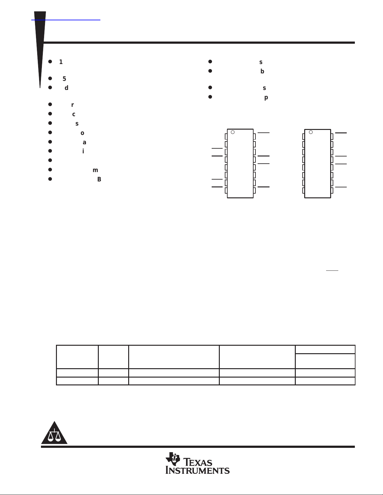
TPS2048
D PACKAGE
(TOP VIEW)
GND1
IN1
EN1
EN2
GND2
IN2
EN3
EN4
1
2
3
4
5
6
7
8
16
15
14
13
12
11
10
9
OC1
OUT1
OUT2
OC2
OC3
OUT3
OUT4
OC4
GND1
IN1
EN1
EN2
GND2
IN2
EN3
EN4
TPS2058
D PACKAGE
(TOP VIEW)
1
2
3
4
5
6
7
8
description
The TPS2048 and TPS2058 quad power-distribution switches are intended for applications where heavy
capacitive loads and short circuits are likely. These devices incorporate in single packages four 135-mΩ
N-channel MOSFET high-side power switches for power-distribution systems that require multiple power
switches. Each switch is controlled by a logic enable compatible with 5-V and 3-V logic. Gate drive is provided
by an internal charge pump that controls the power-switch rise times and fall times to minimize current surges
during switching. The charge pump, requiring no external components, allows operation from supplies as low
as 2.7 V.
16
15
14
13
12
11
10
9
OC1
OUT1
OUT2
OC2
OC3
OUT3
OUT4
OC4
When the output load exceeds the current-limit threshold or a short is present, the TPS2048 and TPS2058 limit
the output current to a safe level by switching into a constant-current mode, pulling the overcurrent (OCx
) logic
output low. When continuous heavy overloads and short circuits increase the power dissipation in the switch
causing the junction temperature to rise, a thermal protection circuit shuts off the switch in overcurrent to prevent
damage. Recovery from a thermal shutdown is automatic once the device has cooled sufficiently. Internal
circuitry ensures the switch remains off until valid input voltage is present.
The TPS2048 and TPS2058 are designed to limit at 0.44-A load. These power-distribution switches are
available in 16-pin small-outline integrated circuit (SOIC) packages and operate over an ambient temperature
range of –40°C to 85°C.
AVAILABLE OPTIONS
RECOMMENDED MAXIMUM TYPICAL SHORT-CIRCUIT
T
A
–40°C to 85°C Active low 0.25 0.44 TPS2048D
–40°C to 85°C Active high 0.25 0.44 TPS2058D
†
The D package is available taped and reeled. Add an R suffix to device type (e.g., TPS2048DR)
Please be aware that an important notice concerning availability, standard warranty, and use in critical applications of
Texas Instruments semiconductor products and disclaimers thereto appears at the end of this data sheet.
ENABLE
CONTINUOUS LOAD CURRENT
(A)
CURRENT LIMIT AT 25°C
(A)
PACKAGED DEVICES
SOIC
†
(D)
PRODUCTION DATA information is current as of publication date.
Products conform to specifications per the terms of Texas Instruments
standard warranty. Production processing does not necessarily include
testing of all parameters.
POST OFFICE BOX 655303 • DALLAS, TEXAS 75265
Copyright 1999, Texas Instruments Incorporated
1
TPS2048, TPS2058
QUAD CURRENT-LIMITED POWER-DISTRIBUTION SWITCHES
SLVS192 – APRIL 1999
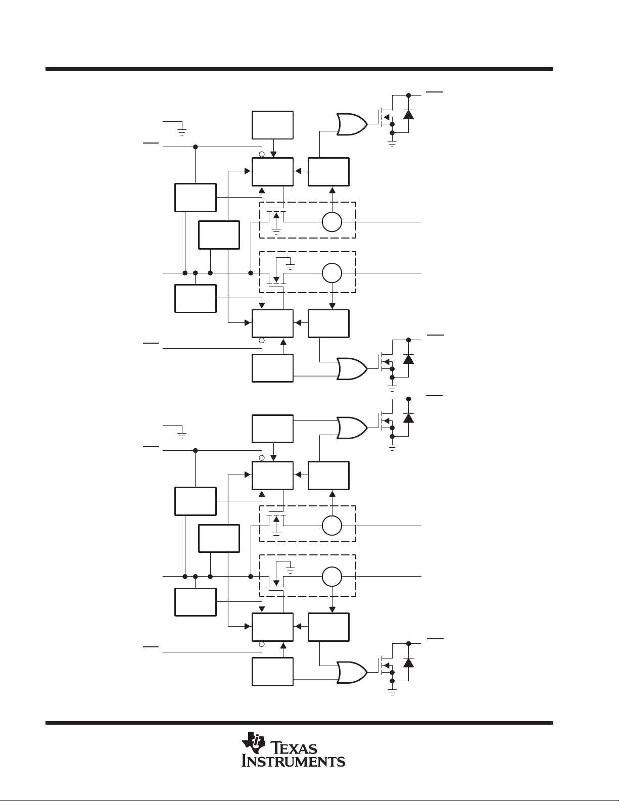
TPS2048 functional block diagram
OC1
GND1
EN1
IN1
EN2
Charge
Pump
Charge
Pump
UVLO
Thermal
Sense
Driver
Driver
Thermal
Sense
Current
Limit
CS
Power Switch
CS
Current
Limit
†
OUT1
†
OUT2
OC2
OC3
GND2
EN3
IN2
EN4
†
Current sense
Charge
Pump
Charge
Pump
UVLO
Thermal
Sense
Driver
Driver
Thermal
Sense
Current
Limit
CS
Power Switch
CS
Current
Limit
†
OUT3
†
OUT4
OC4
2
POST OFFICE BOX 655303 • DALLAS, TEXAS 75265

NAME
QUAD CURRENT-LIMITED POWER-DISTRIBUTION SWITCHES
Terminal Functions
TERMINAL
NO.
TPS2048 TPS2058
EN1 3 – I Enable input. Logic low turns on power switch, IN1-OUT1.
EN2 4 – I Enable input. Logic low turns on power switch, IN1-OUT2.
EN3 7 – I Enable input. Logic low turns on power switch, IN2-OUT3.
EN4 8 – I Enable input. Logic low turns on power switch, IN2-OUT4.
EN1 – 3 I Enable input. Logic high turns on power switch, IN1-OUT1.
EN2 – 4 I Enable input. Logic high turns on power switch, IN1-OUT2.
EN3 – 7 I Enable input. Logic high turns on power switch, IN2-OUT3.
EN4 – 8 I Enable input. Logic high turns on power switch, IN2-OUT4.
GND1 1 1 Ground
GND2 5 5 Ground
IN1 2 2 I Input voltage
IN2 6 6 I Input voltage
OC1 16 16 O Overcurrent. Logic output active low, IN1-OUT1
OC2 13 13 O Overcurrent. Logic output active low, IN1-OUT2
OC3 12 12 O Overcurrent. Logic output active low, IN2-OUT3
OC4 9 9 O Overcurrent. Logic output active low, IN2-OUT4
OUT1 15 15 O Power-switch output, IN1-OUT1
OUT2 14 14 O Power-switch output, IN1-OUT2
OUT3 11 11 O Power-switch output, IN2-OUT3
OUT4 10 10 O Power-switch output, IN2-OUT4
I/O DESCRIPTION
TPS2048, TPS2058
SLVS192 – APRIL 1999
POST OFFICE BOX 655303 • DALLAS, TEXAS 75265
3

TPS2048, TPS2058
QUAD CURRENT-LIMITED POWER-DISTRIBUTION SWITCHES
SLVS192 – APRIL 1999
detailed description
power switch
The power switch is an N-channel MOSFET with a maximum on-state resistance of 135 mΩ (V
Configured as a high-side switch, the power switch prevents current flow from OUTx to INx and INx to OUTx
when disabled. The power switch can supply a minimum of 250 mA per switch.
charge pump
An internal charge pump supplies power to the driver circuit and provides the necessary voltage to pull the gate
of the MOSFET above the source. The charge pump operates from input voltages as low as 2.7 V and requires
very little supply current.
driver
The driver controls the gate voltage of the power switch. T o limit large current surges and reduce the associated
electromagnetic interference (EMI) produced, the driver incorporates circuitry that controls the rise times and
fall times of the output voltage. The rise and fall times are typically in the 2-ms to 4-ms range.
enable (ENx or ENx)
The logic enable disables the power switch and the bias for the charge pump, driver, and other circuitry to reduce
the supply current to less than 20 µA when a logic high is present on ENx (TPS2048) or a logic low is present
on ENx (TPS2058). A logic zero input on ENx or logic high on ENx restores bias to the drive and control circuits
and turns the power on. The enable input is compatible with both TTL and CMOS logic levels.
overcurrent (OCx)
The OCx
encountered. The output will remain asserted until the overcurrent or over temperature condition is removed.
current sense
open drain output is asserted (active low) when an overcurrent or over temperature condition is
I(INx)
= 5 V).
A sense FET monitors the current supplied to the load. The sense FET measures current more efficiently than
conventional resistance methods. When an overload or short circuit is encountered, the current-sense circuitry
sends a control signal to the driver. The driver in turn reduces the gate voltage and drives the power FET into
its saturation region, which switches the output into a constant current mode and holds the current constant
while varying the voltage on the load.
thermal sense
The TPS2048 and TPS2058 implement a dual-threshold thermal trip to allow fully independent operation of the
power distribution switches. In an overcurrent or short-circuit condition the junction temperature rises. When
the die temperature rises to approximately 140°C, the internal thermal sense circuitry checks to determine which
power switch is in an overcurrent condition and turns off that switch, thus, isolating the fault without interrupting
operation of the adjacent power switches. Hysteresis is built into the thermal sense, and after the device has
cooled approximately 20 degrees, the switch turns back on. The switch continues to cycle off and on until the
fault is removed. The (OCx
occurs.
undervoltage lockout
A voltage sense circuit monitors the input voltage. When the input voltage is below approximately 2 V , a control
signal turns off the power switch.
) open-drain output is asserted (active low) when overtemperature or overcurrent
4
POST OFFICE BOX 655303 • DALLAS, TEXAS 75265
UNIT
TPS2048, TPS2058
QUAD CURRENT-LIMITED POWER-DISTRIBUTION SWITCHES
SLVS192 – APRIL 1999
absolute maximum ratings over operating free-air temperature range (unless otherwise noted)
Input voltage range, V
Output voltage range, V
Input voltage range, V
Continuous output current, I
Continuous total power dissipation See Dissipation Rating Table. . . . . . . . . . . . . . . . . . . . . . . . . . . . . . . . . . . . . .
Operating virtual junction temperature range, T
Storage temperature range, T
Lead temperature soldering 1,6 mm (1/16 inch) from case for 10 seconds 260°C. . . . . . . . . . . . . . . . . . . . . . .
Electrostatic discharge (ESD) protection: Human body model MIL-STD-883C 2 kV. . . . . . . . . . . . . . . . . . . . .
†
Stresses beyond those listed under “absolute maximum ratings” may cause permanent damage to the device. These are stress ratings only, and
functional operation of the device at these or any other conditions beyond those indicated under “recommended operating conditions” is not
implied. Exposure to absolute-maximum-rated conditions for extended periods may affect device reliability.
NOTE 1: All voltages are with respect to GND.
PACKAGE
D 725 mW 5.8 mW/°C 464 mW 377 mW
(see Note1) –0.3 V to 6 V. . . . . . . . . . . . . . . . . . . . . . . . . . . . . . . . . . . . . . . . . . . . . . .
I(INx)
O(OUTx)
I(ENx)
(see Note1) –0.3 V to V
or V
I(ENx)
O(OUTx)
J
stg
Machine model 0.2 kV. . . . . . . . . . . . . . . . . . . . . . . . . . . . . . . . . . . . .
DISSIPATION RATING TABLE
TA ≤ 25°C
POWER RATING
DERATING FACTOR
ABOVE TA = 25°C
TA = 70°C
POWER RATING
TA = 85°C
POWER RATING
+ 0.3 V. . . . . . . . . . . . . . . . . . . . . . . . . . . . . . . . . .
I(INx)
–0.3 V to 6 V. . . . . . . . . . . . . . . . . . . . . . . . . . . . . . . . . . . . . . . . . . . . . . . .
Internally limited. . . . . . . . . . . . . . . . . . . . . . . . . . . . . . . . . . . . . . . . . . . . . . . .
–40°C to 125°C. . . . . . . . . . . . . . . . . . . . . . . . . . . . . . . . . . . . . .
–65°C to 150°C. . . . . . . . . . . . . . . . . . . . . . . . . . . . . . . . . . . . . . . . . . . . . . . . . . . .
recommended operating conditions
TPS2048 TPS2058
MIN MAX MIN MAX
Input voltage, V
Input voltage, V
Continuous output current, I
Operating virtual junction temperature, T
I(INx)
I(ENx)
or V
I(ENx)
O(OUTx)
J
2.7 5.5 2.7 5.5 V
0 5.5 0 5.5 V
0 250 0 250 mA
–40 125 –40 125 °C
†
POST OFFICE BOX 655303 • DALLAS, TEXAS 75265
5
TPS2048, TPS2058
PARAMETER
TEST CONDITIONS
†
UNIT
r
trRise time, output
ms
tfFall time, output
ms
PARAMETER
TEST CONDITIONS
UNIT
VILLow–level input voltage
IIInput current
A
PARAMETER
TEST CONDITIONS
†
UNIT
QUAD CURRENT-LIMITED POWER-DISTRIBUTION SWITCHES
SLVS192 – APRIL 1999
electrical characteristics over recommended operating junction temperature range, V
= rated current, V
I
O
I(ENx)
= 0 V, V
= Hi (unless otherwise noted)
I(ENx)
I(INx)
= 5.5 V ,
power switch
TPS2048 TPS2058
MIN TYP MAX MIN TYP MAX
V
= 5 V,
I(INx)
IO = 0.25 A
Static drain-source on-state
resistance, 5-V operation
DS(on)
Static drain-source on-state
resistance, 3.3-V operation
p
p
†
Pulse-testing techniques maintain junction temperature close to ambient temperature; thermal effects must be taken into account separately.
V
= 5 V,
I(INx)
IO = 0.25 A
V
= 5 V,
I(INx)
IO = 0.25 A
V
= 3.3 V,
I(INx)
IO = 0.25 A
V
= 3.3 V,
I(INx)
IO = 0.25 A
V
= 3.3 V,
I(INx)
IO = 0.25 A
V
= 5.5 V,
I(INx)
CL = 1 µF,
V
= 2.7 V,
I(INx)
CL = 1 µF,
V
= 5.5 V,
I(INx)
CL = 1 µF,
V
= 2.7 V,
I(INx)
CL = 1 µF,
TJ = 25°C,
TJ = 85°C,
TJ = 125°C,
TJ = 25°C,
TJ = 85°C,
TJ = 125°C,
TJ = 25°C,
RL = 20 Ω
TJ = 25°C,
RL = 20 Ω
TJ = 25°C,
RL = 20 Ω
TJ = 25°C,
RL = 20 Ω
80 95 80 95
90 120 90 120
100 135 100 135
85 105 85 105
100 135 100 135
115 150 115 150
2.5 2.5
3 3
4.4 4.4
2.5 2.5
mΩ
enable input ENx or ENx
TPS2048 TPS2058
MIN TYP MAX MIN TYP MAX
V
High–level input voltage 2.7 V ≤ V
IH
p
p
t
Turnon time CL = 100 µF, RL = 20 Ω 20 20 ms
on
t
Turnoff time CL = 100 µF, RL = 20 Ω 40 40
off
TPS2048 V
TPS2058 V
4.5 V ≤ V
2.7 V≤ V
I(ENx
I(ENx)
≤ 5.5 V 2 2 V
I(INx)
≤ 5.5 V 0.8 0.8 V
I(INx)
≤ 4.5 V 0.4 0.4
I(INx)
= 0 V or V
)
= V
I(INx)
I(ENx)
or V
= V
I(INx)
= 0 V –0.5 0.5
I(ENx)
–0.5 0.5
µ
current limit
TPS2048 TPS2058
MIN TYP MAX MIN TYP MAX
V
= 5 V, OUT connected to GND,
I
Short-circuit output current
OS
†
Pulse-testing techniques maintain junction temperature close to ambient temperature; thermal effects must be taken into account separately.
I(INx)
Device enable into short circuit
0.345 0.44 0.525 0.345 0.44 0.525 A
6
POST OFFICE BOX 655303 • DALLAS, TEXAS 75265
PARAMETER
TEST CONDITIONS
UNIT
TPS2048
y,
A
V
V
TPS2058
V
V
TPS2048
high-level
A
V
V
TPS2058
g
40°C ≤ T
125°C
A
T
25°C
A
PARAMETER
TEST CONDITIONS
UNIT
PARAMETER
TEST CONDITIONS
UNIT
TPS2048, TPS2058
QUAD CURRENT-LIMITED POWER-DISTRIBUTION SWITCHES
SLVS192 – APRIL 1999
electrical characteristics over recommended operating junction temperature range, V
= rated current, V
I
O
I(ENx)
= 0 V, V
= Hi (unless otherwise noted) (continued)
I(ENx)
I(INx)
= 5.5 V ,
supply current
TPS2048 TPS2058
MIN TYP MAX MIN TYP MAX
Supply current, No Load
low-level output on OUTx
Supply current,
output
Leakage OUTx connected
current to ground
Reverse INx = high
leakage currentgimpedance
No Load
on OUTx
V
V
V
V
V
I(ENx)
I(ENx)
I(ENx)
I(ENx)
I(ENx)
I(ENx)
I(ENx)
I(ENx)
= V
= 0
= 0
=
= V
= 0 V
= 0 V
= Hi
TJ = 25°C
I(INx)
–40°C ≤ TJ ≤ 125°C
TJ = 25°C
–40°C ≤ TJ ≤ 125°C
TJ = 25°C
–40°C ≤ TJ ≤ 125°C
TJ = 25°C
I(INx)
–40°C ≤ TJ ≤ 125°C
I(INx)
–
°
≤
J
°
=
J
TPS2048 200
°
TPS2058 200
TPS2048 0.3
TPS2058 0.3
0.03 2
20
0.03 2
20
160 200
200
160 200
200
undervoltage lockout
TPS2048 TPS2058
MIN TYP MAX MIN TYP MAX
Low-level input voltage 2 2.5 2 2.5 V
Hysteresis TJ = 25°C 100 100 mV
µ
µ
µ
µ
overcurrent OCx
Sink current
Output low voltage IO = 5 mA, V
Off-state current
†
Specified by design, not production tested.
†
†
VO = 5 V 10 10 mA
VO = 5 V, VO = 3.3 V 1 1 µA
OL(OCx
TPS2048 TPS2058
MIN TYP MAX MIN TYP MAX
)
0.5 0.5 V
POST OFFICE BOX 655303 • DALLAS, TEXAS 75265
7
TPS2048, TPS2058
QUAD CURRENT-LIMITED POWER-DISTRIBUTION SWITCHES
SLVS192 – APRIL 1999
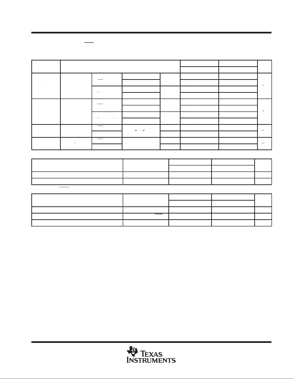
PARAMETER MEASUREMENT INFORMATION
OUTx
V
I(ENx)
(5 V/div)
V
I(ENx)
V
O(OUTx)
t
RL CL
V
O(OUTx)
TEST CIRCUIT
50%
t
on
50%
90%
10%
V
I(ENx)
t
off
V
O(OUTx)
VOLTAGE WA VEFORMS
r
90%
90%
10%
50%
t
on
10%
50%
90%
10%
t
f
t
off
Figure 1. Test Circuit and Voltage Waveforms
V
I(ENx)
(5 V/div)
V
O(OUTx)
(2 V/div)
8
V
= 5 V
I(INx)
TA = 25°C
CL = 0.1 µF
0123456
t – Time – ms
78910
Figure 2. Turnon Delay and Rise Time
with 0.1-µF Load
POST OFFICE BOX 655303 • DALLAS, TEXAS 75265
V
O(OUTx)
(2 V/div)
V
= 5 V
I(INx)
TA = 25°C
CL = 0.1 µF
0 1000 2000 3000
t – Time – ms
4000 5000
Figure 3. Turnoff Delay and Fall Time
with 0.1-µF Load

V
V
I(ENx)
(5 V/div)
O(OUTx)
(2 V/div)
QUAD CURRENT-LIMITED POWER-DISTRIBUTION SWITCHES
PARAMETER MEASUREMENT INFORMATION
012345 6
t – Time – ms
V
= 5 V
I(INx)
TA = 25°C
CL = 1 µF
RL = 20 Ω
78910
V
I(ENx)
(5 V/div)
V
O(OUTx)
(2 V/div)
TPS2048, TPS2058
V
= 5 V
I(INx)
TA = 25°C
CL = 1 µF
RL = 20 Ω
0 2 4 6 8 10 12
t – Time – ms
SLVS192 – APRIL 1999
14 16 18 20
Figure 4. Turnon Delay and Rise Time
with 1-µF Load
V
I(ENx)
(5 V/div)
I
O(OUTx)
(0.2 A/div)
012345 6
t – Time – ms
Figure 6. TPS2048, Short-Circuit Current,
Device Enabled into Short
V
= 5 V
I(INx)
TA = 25°C
78910
Figure 5. Turnoff Delay and Fall Time
with 1-µF Load
V
= 5 V
I(INx)
TA = 25°C
V
O(OUTx)
(2 V/div)
I
O(OUTx)
(0.5 A/div)
01020 30405060
t – Time – ms
Figure 7. TPS2048, Threshold Trip Current
with Ramped Load on Enabled Device
70 80 90 100
POST OFFICE BOX 655303 • DALLAS, TEXAS 75265
9

TPS2048, TPS2058
QUAD CURRENT-LIMITED POWER-DISTRIBUTION SWITCHES
SLVS192 – APRIL 1999
PARAMETER MEASUREMENT INFORMATION
V
= 5 V
I(INx)
TA = 25°C
RL = 20 Ω
V
I(ENx)
(5 V/div)
I
O(OUTx)
(0.2 A/div)
Figure 8. Inrush Current with 220-µF, 100-µF
V
O(OCx)
(5 V/div)
220 µF
47 µF
0 2 4 6 8 10 12
100 µF
t – Time – ms
and 47-µF Load Capacitance
14 16 18 20
V
= 5 V
I(INx)
TA = 25°C
V
O(OCx)
(5 V/div)
I
O(OUTx)
(0.5 A/div)
Figure 9. Ramped Load on Enabled Device
V
O(OCx)
(5 V/div)
0 20 40 60 80 100 120
t – Time – ms
V
= 5 V
I(INx)
TA = 25°C
140 160 180 200
V
= 5 V
I(INx)
TA = 25°C
I
O(OUTx)
(0.5 A/div)
10
0 200 400 600 800 1000
t – Time – µs
Figure 10. 4-Ω Load Connected
to Enabled Device
POST OFFICE BOX 655303 • DALLAS, TEXAS 75265
I
O(OUTx)
(0.5 A/div)
0 200 400 600 800 1000
t – Time – µs
Figure 11. 1-Ω Load Connected
to Enabled Device

TPS2048, TPS2058
QUAD CURRENT-LIMITED POWER-DISTRIBUTION SWITCHES
SLVS192 – APRIL 1999
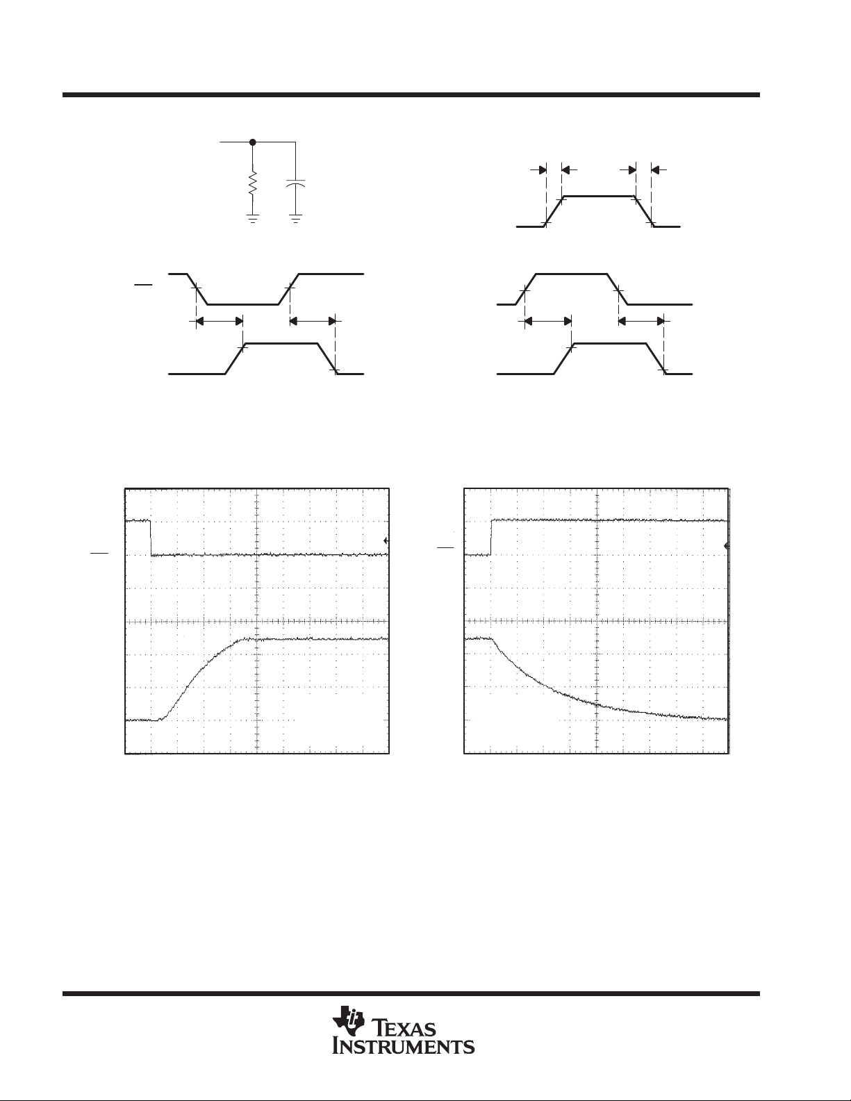
TYPICAL CHARACTERISTICS
6
5.5
5
4.5
Turnon Delay – ms
4
3.5
3
2.5 3 3.5 4 4.5
2.7
VI
= 5 V
(INx)
TA = 25°C
TURNON DELAY
vs
INPUT VOLTAGE
VI – Input Voltage – V
Figure 12
RISE TIME
vs
LOAD CURRENT
CL = 1 µF
RL = 20 Ω
TA = 25°C
5 5.5 6
15
CL = 1 µF
RL = 20 Ω
TA = 25°C
13
11
Turnoff Delay – ms
9
7
2.5 3 3.5 4 4.5
VI – Input Voltage – V
2.85
VI
= 5 V
(INx)
TA = 25°C
TURNOFF DELAY
vs
INPUT VOLTAGE
5 5.5 6
Figure 13
FALL TIME
vs
LOAD CURRENT
2.6
2.5
– Rise Time – ms
r
t
2.4
2.3
0 0.05 0.1 0.15 0.2 0.25
IL – Load Current – A
Figure 14
2.8
2.75
– Fall Time – ms
f
t
2.7
0.3 0.35 0.4
POST OFFICE BOX 655303 • DALLAS, TEXAS 75265
2.65
0 0.05 0.1 0.15 0.2 0.25
0.3 0.35 0.4
IL – Load Current – A
Figure 15
11
TPS2048, TPS2058
QUAD CURRENT-LIMITED POWER-DISTRIBUTION SWITCHES
SLVS192 – APRIL 1999
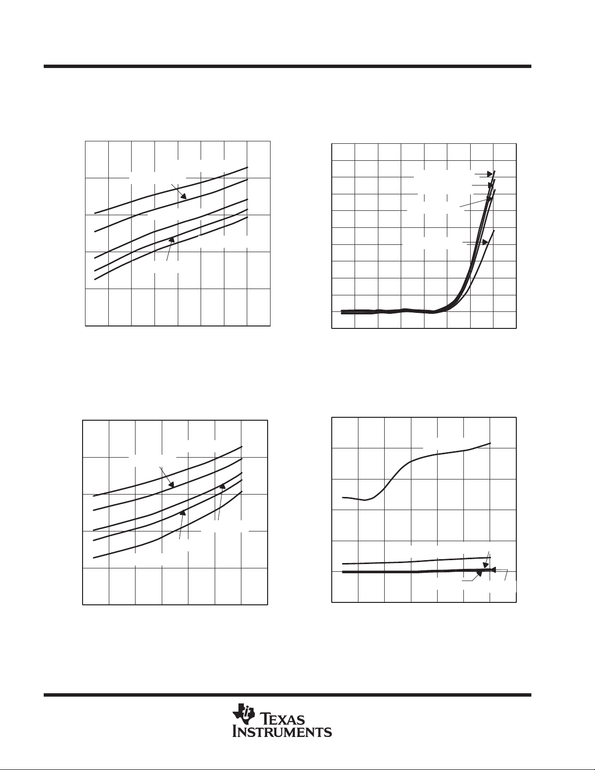
TYPICAL CHARACTERISTICS
SUPPLY CURRENT, OUTPUT ENABLED
vs
JUNCTION TEMPERATURE
200
Aµ
V
180
160
140
120
– Supply Current, Output Enabled –
I(INx)
I
100
–50 –25 0 25 50
TJ – Junction Temperature – °C
I(INx)
V
I(INx)
= 5 V
V
I(INx)
= 3.3 V
Figure 16
SUPPLY CURRENT, OUTPUT ENABLED
vs
INPUT VOLTAGE
200
Aµ
180
TJ = 85°C
V
= 5.5 V
I(INx)
= 4 V
V
= 2.7 V
I(INx)
75 100 125 150
TJ = 125°C
SUPPLY CURRENT, OUTPUT DISABLED
vs
JUNCTION TEMPERATURE
2000
1800
V
V
I(INx)
V
I(INx)
V
I(INx)
I(INx)
= 4 V
= 2.7 V
1600
1400
1200
1000
800
600
400
– Supply Current, Output Disabled – nA
200
0
I(INx)
I
–200
–50 –25 0 25 50 75
TJ – Junction Temperature – °C
Figure 17
SUPPLY CURRENT, OUTPUT DISABLED
vs
INPUT VOLTAGE
2000
1600
TJ = 125°C
= 5.5 V
= 5 V
100 125 150
160
140
120
– Supply Current, Output Enabled –
I(INx)
I
100
2.5 3 3.5 4
TJ = –40°C
VI – Input Voltage – V
Figure 18
12
TJ = 0°C
4.5
1200
800
TJ = 25°C
400
– Supply Current, Output Disabled – nA
0
I(INx)
I
–400
5 5.5 6
POST OFFICE BOX 655303 • DALLAS, TEXAS 75265
2.5 3 3.5 4 4.5
TJ = 85°C
TJ = –40°C
VI – Input Voltage – V
Figure 19
TJ = 25°C
TJ = 0°C
5 5.5 6
TPS2048, TPS2058
QUAD CURRENT-LIMITED POWER-DISTRIBUTION SWITCHES
SLVS192 – APRIL 1999
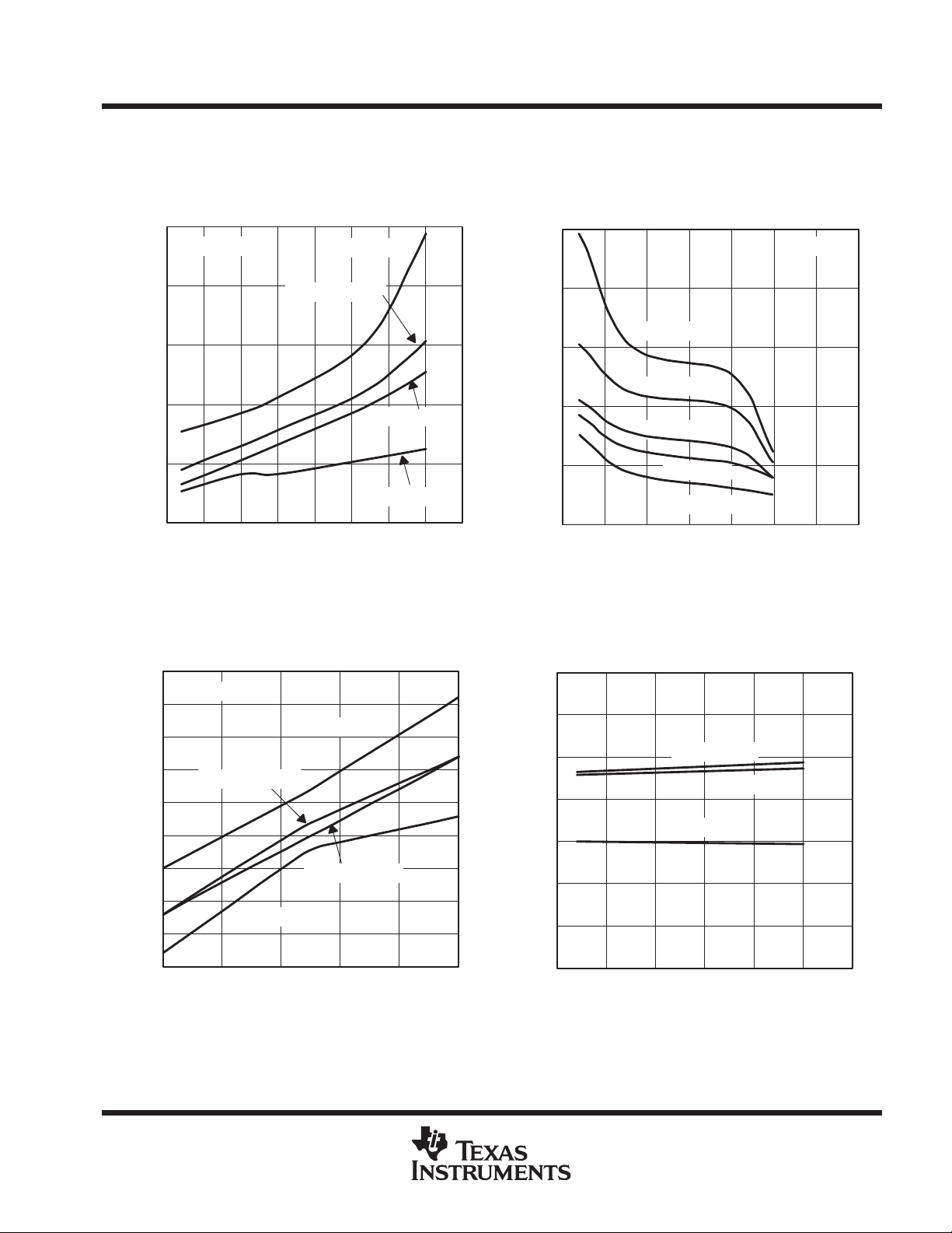
TYPICAL CHARACTERISTICS
STATIC DRAIN-SOURCE ON-STATE RESISTANCE
vs
Ω
175
150
125
100
75
– Static Drain-Source On-State Resistance – m
50
–50 –25 0 25 50 75
DS(on)
r
JUNCTION TEMPERATURE
IO = 0.25 A
V
I(INx)
TJ – Junction Temperature –°C
V
I(INx)
= 3.3 V
= 2.7 V
V
I(INx)
V
I(INx)
100 125 150
Figure 20
INPUT-TO-OUTPUT VOLTAGE
vs
LOAD CURRENT
45
TA = 25°C
40
V
= 2.7 V
= 5 V
I(INx)
V
I(INx)
= 4.5 V
35
30
25
20
– Input-To-Output Voltage – mV
15
10
O(OUTx)
V
–
5
V
I(INx)
= 3.3 V
V
I(INx)
= 4.5 V
= 5 V
STATIC DRAIN-SOURCE ON-STATE RESISTANCE
vs
Ω
175
150
125
100
75
– Static Drain-Source On-State Resistance – m
50
DS(on)
2.5 3 3.5 4 4.5
r
INPUT VOLTAGE
IO = 0.25 A
TJ = 125°C
TJ = 85°C
TJ = 25°C
TJ = 0°C
TJ = –40°C
5 5.5 6
VI – Input Voltage – V
Figure 21
SHORT-CURCUIT OUTPUT CURRENT
vs
INPUT VOLTAGE
490
470
450
430
410
390
– Short-circuit Output Current – mA
370
OS
I
TJ = –40°C
TJ = 25°C
TJ = 125°C
I(INx)
0
V
0.1 0.14 0.18
0.22 0.3
IL – Load Current – A
Figure 22
0.26
POST OFFICE BOX 655303 • DALLAS, TEXAS 75265
350
2.5 3 3.5 4
4.5 5 5.5
VI – Input Voltage – V
Figure 23
13

TPS2048, TPS2058
QUAD CURRENT-LIMITED POWER-DISTRIBUTION SWITCHES
SLVS192 – APRIL 1999
TYPICAL CHARACTERISTICS
0.73
TA = 25°C
Load Ramp = 1 A/10 ms
0.71
0.69
0.67
Threshold Trip Current – A
0.65
2.5 3 3.5 4
2.5
2.4
2.3
THRESHOLD TRIP CURRENT
vs
INPUT VOLTAGE
4.5 5 65.5
VI – Input Voltage – V
Figure 24
UNDERVOLTAGE LOCKOUT
vs
JUNCTION TEMPERATURE
Start Threshold
SHORTCIRCUIT OUTPUT CURRENT
vs
JUNCTION TEMPERATURE
450
V
V
I(INx)
I(INx)
445
440
V
= 4 V
435
430
425
420
415
– Short-circuit Output Current – mA
OS
I
410
405
–50 –25 0 25 50
I(INx)
TJ – Junction Temperature – °C
Figure 25
CURRENT-LIMIT RESPONSE
vs
PEAK CURRENT
500
sµ
350
= 5 V
= 2.7 V
75 100 125
V
I(INx)
TA = 25°C
= 5 V
2.2
2.1
UVLO – Undervoltage Lockout – V
2
–50 –25 0 25 50 75
TJ – Junction Temperature – °C
Figure 26
14
Stop Threshold
250
Current Limit Response –
100
100 125 150
POST OFFICE BOX 655303 • DALLAS, TEXAS 75265
0
02 4 6
810
Peak Current – A
Figure 27
TPS2048, TPS2058
QUAD CURRENT-LIMITED POWER-DISTRIBUTION SWITCHES
SLVS192 – APRIL 1999
TYPICAL CHARACTERISTICS
OVERCURRENT (OCx) RESPONSE TIME
vs
PEAK CURRENT
10
V
= 5 V
I(INx)
TA = 25°C
sµ
8.5
7
5.5
Overcurrent OCx Time –
Power Supply
2.7 V to 5.5 V
4
0246
Peak Current – A
Figure 28
APPLICATION INFORMATION
2
IN1
16
13
12
6
IN2
OC1
OC2
OC3
9
OC4
3
EN1
4
7
EN3
8
EN4
OUT1
OUT2
OUT3
OUT4
GND1
GND2
810
15
0.1 µF 22 µF
14
0.1 µF 22 µF
11
0.1 µF 22 µF
10EN2
0.1 µF 22 µF
1
5
Load
Load
Load
Load
Figure 29. Typical Application
POST OFFICE BOX 655303 • DALLAS, TEXAS 75265
15

TPS2048, TPS2058
QUAD CURRENT-LIMITED POWER-DISTRIBUTION SWITCHES
SLVS192 – APRIL 1999
APPLICATION INFORMATION
power supply considerations
A 0.01-µF to 0.1-µF ceramic bypass capacitor between IN and GND, close to the device, is recommended.
Placing a high-value electrolytic capacitor on the output pin(s) is recommended when the output load is heavy .
This precaution reduces power-supply transients that may cause ringing on the input. Additionally , bypassing
the output with a 0.01-µF to 0.1-µF ceramic capacitor improves the immunity of the device to short-circuit
transients.
overcurrent
A sense FET checks for overcurrent conditions. Unlike current-sense resistors, sense FET s do not increase the
series resistance of the current path. When an overcurrent condition is detected, the device maintains a
constant output current and reduces the output voltage accordingly . Complete shutdown occurs only if the fault
is present long enough to activate thermal limiting.
Three possible overload conditions can occur. In the first condition, the output has been shorted before the
device is enabled or before V
and immediately switch into a constant-current output.
has been applied (see Figure 6). The TPS2048 and TPS2058 sense the short
I(INx)
In the second condition, the short occurs while the device is enabled. At the instant the short occurs, very high
currents may flow for a short time before the current-limit circuit can react . After the current-limit circuit has
tripped (reached the overcurrent trip threshhold) the device switches into constant-current mode.
In the third condition, the load has been gradually increased beyond the recommended operating current. The
current is permitted to rise until the current-limit threshold is reached or until the thermal limit of the device is
exceeded (see Figure 7). The TPS2048 and TPS2058 are capable of delivering current up to the current-limit
threshold without damaging the device. Once the threshold has been reached, the device switches into its
constant-current mode.
OC response
The OC open-drain output is asserted (active low) when an overcurrent or overtemperature condition is
encountered. The output will remain asserted until the overcurrent or overtemperature condition is removed.
Connecting a heavy capacitive load to an enabled device can cause momentary false overcurrent reporting from
the inrush current flowing through the device, charging the downstream capacitor. An RC filter of 500 µs (see
Figure 30) can be connected to OCx
or extremly high capacitive loads. Using low-ESR electrolytic capacitors on the output lowers the inrush current
flow through the device during hot-plug events by providing a low impedance energy source, thereby reducing
erroneous overcurrent reporting.
to reduce false overcurrent reporting caused by hot-plug switching events
16
POST OFFICE BOX 655303 • DALLAS, TEXAS 75265

TPS2048, TPS2058
QUAD CURRENT-LIMITED POWER-DISTRIBUTION SWITCHES
SLVS192 – APRIL 1999
APPLICATION INFORMATION
GND1
IN1
EN1
EN2
GND2
IN2
EN3
EN4
TPS2048
OC1
OUT1
OUT2
OC2
OC3
OUT3
OUT4
OC4
V+
R
pullup
GND1
IN1
EN1
EN2
GND2
IN2
EN3
EN4
TPS2048
OUT1
OUT2
OUT3
OUT4
OC1
OC2
OC3
OC4
V+
R
pullup
R
filter
To USB
Controller
C
filter
Figure 30. Typical Circuit for OC Pin and RC Filter for Damping Inrush OC Responses
power dissipation and junction temperature
The low on-resistance on the n-channel MOSFET allows small surface-mount packages, such as SOIC, to pass
large currents. The thermal resistances of these packages are high compared to those of power packages; it
is good design practice to check power dissipation and junction temperature. The first step is to find r
the input voltage and operating temperature. As an initial estimate, use the highest operating ambient
temperature of interest and read r
P
+
r
D
DS(on
2
I
)
from Figure 21. Next, calculate the power dissipation using:
DS(on)
DS(on)
at
Finally, calculate the junction temperature:
T
+
P
R
)
JA
T
A
J
q
D
Where:
TA = Ambient Temperature °C
R
= Thermal resistance SOIC = 172°C/W
θJA
Compare the calculated junction temperature with the initial estimate. If they do not agree within a few degrees,
repeat the calculation, using the calculated value as the new estimate. Two or three iterations are generally
sufficient to get a reasonable answer.
POST OFFICE BOX 655303 • DALLAS, TEXAS 75265
17

TPS2048, TPS2058
QUAD CURRENT-LIMITED POWER-DISTRIBUTION SWITCHES
SLVS192 – APRIL 1999
APPLICATION INFORMATION
thermal protection
Thermal protection prevents damage to the IC when heavy-overload or short-circuit faults are present for
extended periods of time. The faults force the TPS2048 and TPS2058 into constant current mode, which causes
the voltage across the high-side switch to increase; under short-circuit conditions, the voltage across the switch
is equal to the input voltage. The increased dissipation causes the junction temperature to rise to high levels.
The protection circuit senses the junction temperature of the switch and shuts it off. Hysteresis is built into the
thermal sense circuit, and after the device has cooled approximately 20 degrees, the switch turns back on. The
switch continues to cycle in this manner until the load fault or input power is removed.
The TPS2048 and TPS2058 implement a dual thermal trip to allow fully independent operation of the power
distribution switches. In an overcurrent or short-circuit condition the junction temperature will rise. Once the die
temperature rises to approximately 140°C, the internal thermal sense circuitry checks which power switch is
in an overcurrent condition and turns that power switch off, thus isolating the fault without interrupting operation
of the adjacent power switch. Should the die temperature exceed the first thermal trip point of 140°C and reach
160°C, both switches turn off. The OC
overcurrent occurs.
open-drain output is asserted (active low) when overtemperature or
undervoltage lockout (UVLO)
An undervoltage lockout ensures that the power switch is in the off state at power up. Whenever the input voltage
falls below approximately 2 V, the power switch will be quickly turned off. This facilitates the design of
hot-insertion systems where it is not possible to turn off the power switch before input power is removed. The
UVLO will also keep the switch from being turned on until the power supply has reached at least 2 V, even if
the switch is enabled. Upon reinsertion, the power switch will be turned on with a controlled rise time to reduce
EMI and voltage overshoots.
Universal Serial Bus (USB) applications
The universal serial bus (USB) interface is a 12-Mb/s, or 1.5-Mb/s, multiplexed serial bus designed for
low-to-medium bandwidth PC peripherals (e.g., keyboards, printers, scanners, and mice). The four-wire USB
interface is conceived for dynamic attach-detach (hot plug-unplug) of peripherals. Two lines are provided for
differential data, and two lines are provided for 5-V power distribution.
USB data is a 3.3-V level signal, but power is distributed at 5 V to allow for voltage drops in cases where power
is distributed through more than one hub across long cables. Each function must provide its own regulated 3.3 V
from the 5-V input or its own internal power supply.
The USB specification defines the following five classes of devices, each differentiated by power-consumption
requirements:
D
Hosts/self-powered hubs (SPH)
D
Bus-powered hubs (BPH)
D
Low-power, bus-powered functions
D
High-power, bus-powered functions
D
Self-powered functions
Bus-powered hubs distribute data and power to downstream functions. The TPS2048 and TPS2058 can
provide power-distribution solutions for many of these classes of devices.
18
POST OFFICE BOX 655303 • DALLAS, TEXAS 75265

TPS2048, TPS2058
QUAD CURRENT-LIMITED POWER-DISTRIBUTION SWITCHES
SLVS192 – APRIL 1999
APPLICATION INFORMATION
bus-powered hubs
Bus-powered hubs obtain all power from upstream ports and often contain an embedded function. The hubs
are required to power up with less than one unit load. The BPH usually has one embedded function, and power
is always available to the controller of the hub. If the embedded function and hub require more than 100 mA
on power up, the power to the embedded function may need to be kept off until enumeration is completed. This
can be accomplished by removing power or by shutting off the clock to the embedded function. Power switching
the embedded function is not necessary if the aggregate power draw for the function and controller is less than
one unit load. The total current drawn by the bus-powered device is the sum of the current to the controller, the
embedded function, and the downstream ports, and it is limited to 500 mA from an upstream port.
low-power bus-powered functions and high-power bus-powered functions
Both low-power and high-power bus-powered functions obtain all power from upstream ports; low-power
functions always draw less than 100 mA, and high-power functions must draw less than 100 mA at power up
and can draw up to 500 mA after enumeration. If the load of the function is more than the parallel combination
of 44 Ω and 10 µF at power up, the device must implement inrush current limiting (see Figure 31).
Power Supply
3.3 V
10 µF
0.1 µF
TPS2048
2
IN1
6
IN2
OUT1
15
0.1 µF 10 µF
Internal
Function
V
BUS
GND
D+
D–
USB
Control
14
0.1 µF 10 µF
11
0.1 µF 10 µF
10
0.1 µF 10 µF
1
5
16
13
12
3
EN1
4
EN2
7
EN3
8
EN4
OC1
OC2
OC3
9
OC4
OUT2
OUT3
OUT4
GND1
GND2
Figure 31. High-Power Bus-Powered Function
Internal
Function
Internal
Function
Internal
Function
POST OFFICE BOX 655303 • DALLAS, TEXAS 75265
19

TPS2048, TPS2058
QUAD CURRENT-LIMITED POWER-DISTRIBUTION SWITCHES
SLVS192 – APRIL 1999
APPLICATION INFORMATION
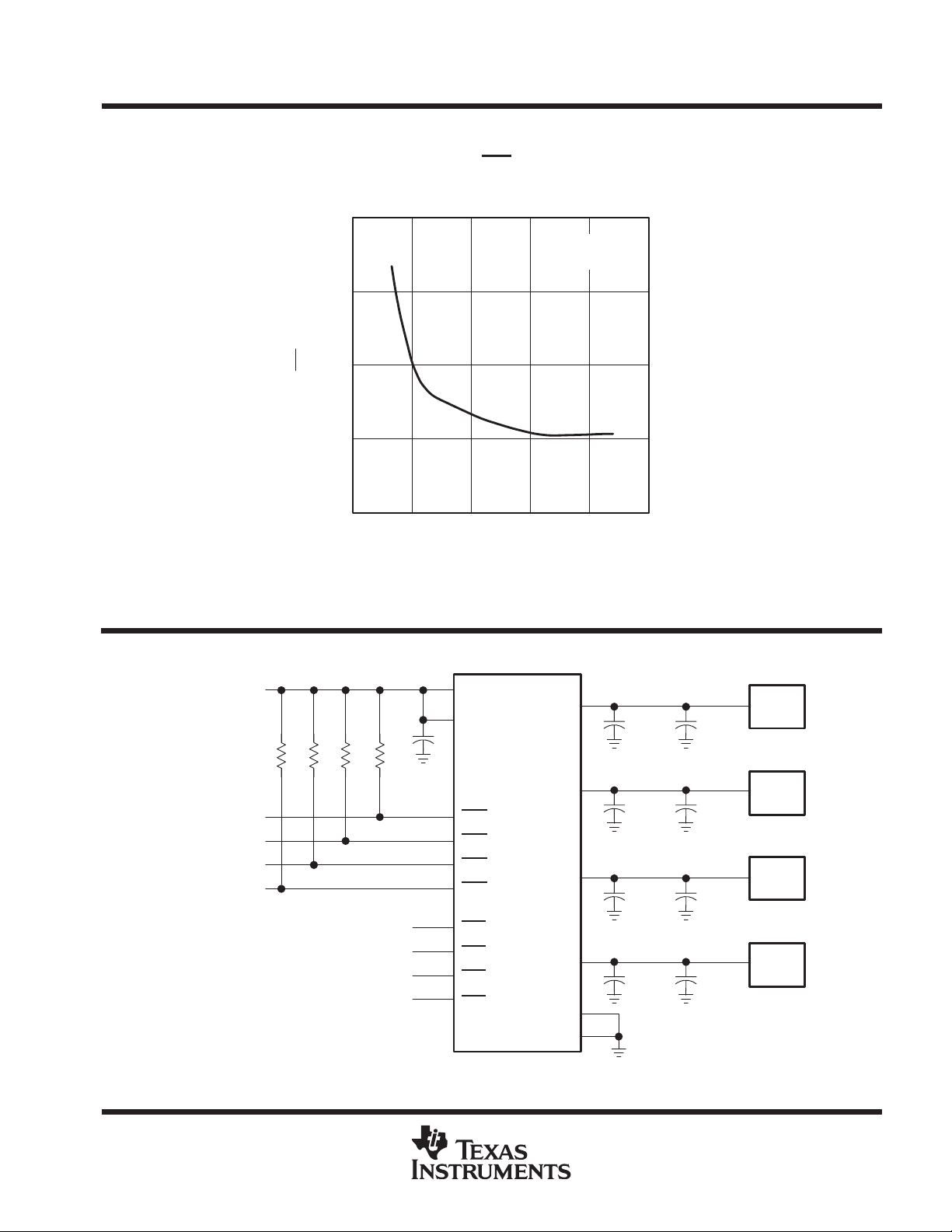
USB power-distribution requirements
USB can be implemented in several ways, and, regardless of the type of USB device being developed, several
power distribution features must be implemented.
D
Bus-Powered Hubs must:
– Enable/disable power to downstream ports
– Power up at <100 mA
– Limit inrush current (<44 Ω and 10 µF)
D
Functions must:
– Limit inrush currents
– Power up at <100 mA
The feature set of the TPS2048 and TPS2058 allows them to meet each of these requirements. The integrated
current-limiting and overcurrent reporting is required by hosts and self-powered hubs. The logic-level enable
and controlled rise times meet the need of both input and output ports on bus-power hubs, as well as the input
ports for bus-power functions (see Figure 32).
20
POST OFFICE BOX 655303 • DALLAS, TEXAS 75265

TPS2048, TPS2058
QUAD CURRENT-LIMITED POWER-DISTRIBUTION SWITCHES
SLVS192 – APRIL 1999
APPLICATION INFORMATION
TUSB2040
Hub Controller
Upstream
Port
D +
D –
GND
5 V
1 µF
SN75240
A
B
0.1 µF
4.7 µF
C
D
GND
TPS76333
IN
3.3 V
GND
48-MHz
Crystal
Tuning
Circuit
4.7 µF
DP0
DM0
V
CC
XTAL1
XTAL2
OCSOFF
GND
BUSPWR
GANGED
DP1
DM1
DP2
DM2
DP3
DM3
DP4
DM4
PWRON1
OVRCUR1
PWRON2
OVRCUR2
PWRON3
OVRCUR3
PWRON4
OVRCUR4
TPS2048
EN1
OC1
EN2
OC2
EN3
OC3
EN4
OC4
OUT1
OUT2
IN1
OUT3
OUT4
IN2
GND1
GND2
ABC
D
SN75240
ABC
D
SN75240
0.1 µF
0.1 µF
Ferrite Beads
Ferrite Beads
Ferrite Beads
Ferrite Beads
Downstream
Ports
D +
D –
GND
5 V
†
33 µF
D +
D –
GND
5 V
†
33 µF
D +
D –
GND
5 V
†
33 µF
D +
D –
GND
5 V
†
USB rev 1.1 requires 120 µF per hub.
Figure 32. Bus-Powered Hub Implementation
POST OFFICE BOX 655303 • DALLAS, TEXAS 75265
33 µF
†
21

TPS2048, TPS2058
QUAD CURRENT-LIMITED POWER-DISTRIBUTION SWITCHES
SLVS192 – APRIL 1999
APPLICATION INFORMATION
generic hot-plug applications (see Figure 33)
In many applications it may be necessary to remove modules or pc boards while the main unit is still operating.
These are considered hot-plug applications. Such implementations require the control of current surges seen
by the main power supply and the card being inserted. The most effective way to control these surges is to limit
and slowly ramp the current and voltage being applied to the card, similar to the way in which a power supply
normally turns on. Due to the controlled rise times and fall times of the TPS2048 and TPS2058, these devices
can be used to provide a softer start-up to devices being hot-plugged into a powered system. The UVLO feature
of the TPS2048 and TPS2058 also ensures the switch will be off after the card has been removed, and the switch
will be off during the next insertion. The UVLO feature guarantees a soft start with a controlled rise time for every
insertion of the card or module.
PC Board
TPS2048
Power
Supply
2.7 V to 5.5 V
1000 µF
Optimum
0.1 µF
GND1
IN1
EN1
GND2
IN2
EN3
EN4
OC1
OUT1
OUT2
OC2EN2
OC3
OUT3
OUT4
OC4
Block of
Circuitry
Block of
Circuitry
Block of
Circuitry
Block of
Circuitry
Overcurrent Response
Figure 33. Typical Hot-Plug Implementation
By placing the TPS2048 or TPS2058 between the VCC input and the rest of the circuitry, the input power will
reach these devices first after insertion. The typical rise time of the switch is approximately 2.5 ms, providing
a slow voltage ramp at the output of the device. This implementation controls system surge currents and
provides a hot-plugging mechanism for any device.
22
POST OFFICE BOX 655303 • DALLAS, TEXAS 75265

TPS2048, TPS2058
QUAD CURRENT-LIMITED POWER-DISTRIBUTION SWITCHES
SLVS192 – APRIL 1999
MECHANICAL DATA
D (R-PDSO-G**) PLASTIC SMALL-OUTLINE PACKAGE
14 PIN SHOWN
0.050 (1,27)
14
1
0.069 (1,75) MAX
0.020 (0,51)
0.014 (0,35)
8
7
A
0.010 (0,25)
0.004 (0,10)
DIM
0.157 (4,00)
0.150 (3,81)
PINS **
0.010 (0,25)
0.244 (6,20)
0.228 (5,80)
8
M
Seating Plane
0.004 (0,10)
14
0.008 (0,20) NOM
0°–8°
16
Gage Plane
0.010 (0,25)
0.044 (1,12)
0.016 (0,40)
A MAX
A MIN
NOTES: A. All linear dimensions are in inches (millimeters).
B. This drawing is subject to change without notice.
C. Body dimensions do not include mold flash or protrusion, not to exceed 0.006 (0,15).
D. Falls within JEDEC MS-012
POST OFFICE BOX 655303 • DALLAS, TEXAS 75265
0.197
(5,00)
0.189
(4,80)
0.344
(8,75)
0.337
(8,55)
0.394
(10,00)
0.386
(9,80)
4040047/D 10/96
23

IMPORTANT NOTICE
T exas Instruments and its subsidiaries (TI) reserve the right to make changes to their products or to discontinue
any product or service without notice, and advise customers to obtain the latest version of relevant information
to verify, before placing orders, that information being relied on is current and complete. All products are sold
subject to the terms and conditions of sale supplied at the time of order acknowledgement, including those
pertaining to warranty, patent infringement, and limitation of liability.
TI warrants performance of its semiconductor products to the specifications applicable at the time of sale in
accordance with TI’s standard warranty. Testing and other quality control techniques are utilized to the extent
TI deems necessary to support this warranty . Specific testing of all parameters of each device is not necessarily
performed, except those mandated by government requirements.
CERTAIN APPLICATIONS USING SEMICONDUCTOR PRODUCTS MAY INVOLVE POTENTIAL RISKS OF
DEATH, PERSONAL INJURY, OR SEVERE PROPERTY OR ENVIRONMENTAL DAMAGE (“CRITICAL
APPLICATIONS”). TI SEMICONDUCTOR PRODUCTS ARE NOT DESIGNED, AUTHORIZED, OR
WARRANTED TO BE SUITABLE FOR USE IN LIFE-SUPPORT DEVICES OR SYSTEMS OR OTHER
CRITICAL APPLICA TIONS. INCLUSION OF TI PRODUCTS IN SUCH APPLICATIONS IS UNDERST OOD TO
BE FULLY AT THE CUSTOMER’S RISK.
In order to minimize risks associated with the customer’s applications, adequate design and operating
safeguards must be provided by the customer to minimize inherent or procedural hazards.
TI assumes no liability for applications assistance or customer product design. TI does not warrant or represent
that any license, either express or implied, is granted under any patent right, copyright, mask work right, or other
intellectual property right of TI covering or relating to any combination, machine, or process in which such
semiconductor products or services might be or are used. TI’s publication of information regarding any third
party’s products or services does not constitute TI’s approval, warranty or endorsement thereof.
Copyright 1999, Texas Instruments Incorporated
 Loading...