

查询TPS2010A供应商
D
33-mΩ (5-V Input) High-Side MOSFET
Switch
D
Short-Circuit and Thermal Protection
D
Operating Range . . . 2.7 V to 5.5 V
D
Logic-Level Enable Input
D
Typical Rise Time . . . 6.1 ms
D
Undervoltage Lockout
D
Maximum Standby Supply
Current ...10 µA
D
No Drain-Source Back-Gate Diode
D
Available in 8-pin SOIC and 14-Pin TSSOP
Packages
D
Ambient Temperature Range, –40°C to 85°C
D
2-kV Human-Body-Model, 200-V
Machine-Model ESD Protection
description
TPS2010A, TPS2011A, TPS2012A, TPS2013A
POWER-DISTRIBUTION SWITCHES
SLVS189A – DECEMBER 1998 – REVISED NOVEMBER 1999
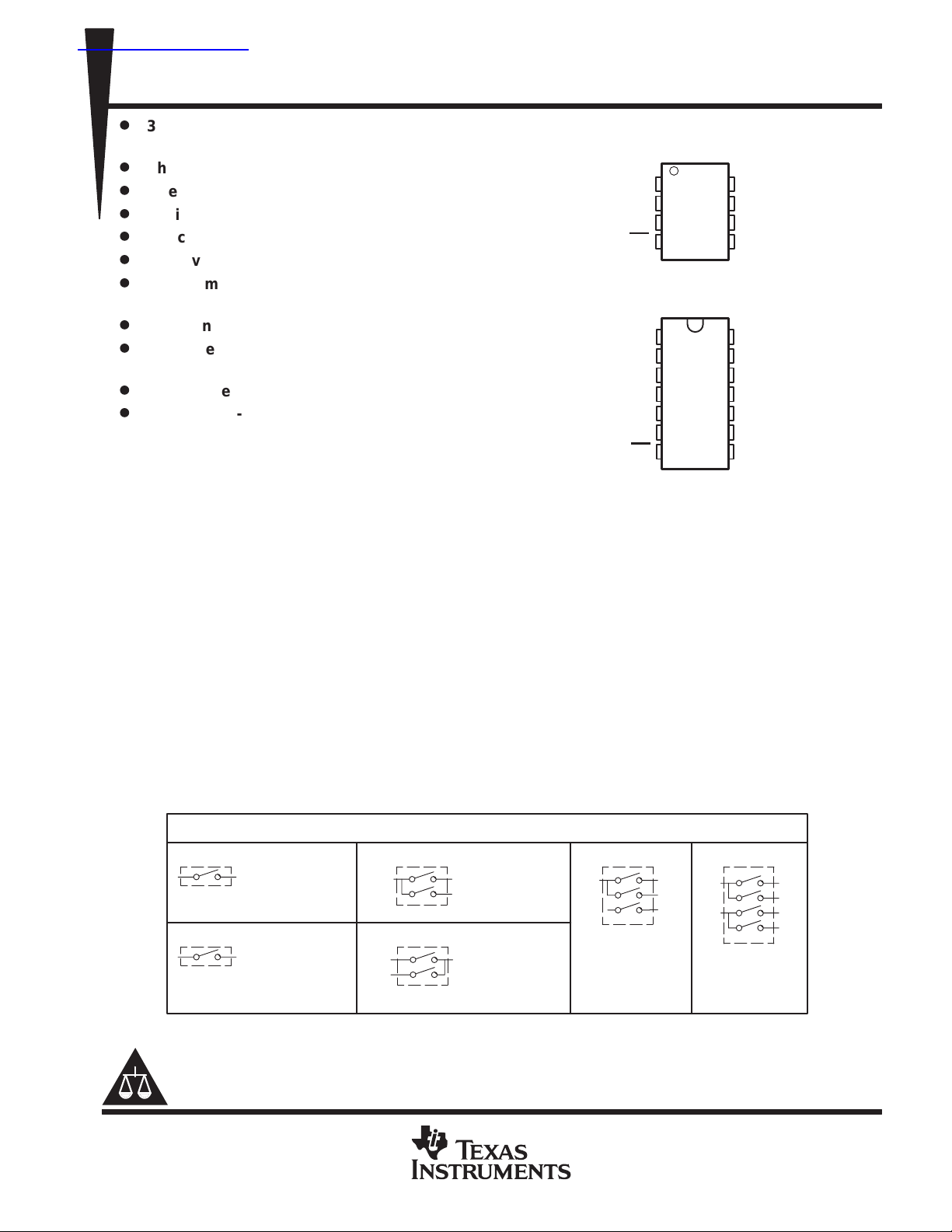
D PACKAGE
(TOP VIEW)
GND
IN
IN
EN
PWP PACKAGE
(TOP VIEW)
GND
IN
IN
IN
IN
IN
EN
1
2
3
4
1
2
3
4
5
6
7
14
13
12
11
10
OUT
8
OUT
7
OUT
6
5
OUT
OUT
OUT
OUT
OUT
OUT
OUT
9
OUT
8
The TPS201xA family of power distribution switches is intended for applications where heavy capacitive loads
and short circuits are likely to be encountered. These devices are 50-mΩ N-channel MOSFET high-side power
switches. The switch is controlled by a logic enable compatible with 5-V logic and 3-V logic. Gate drive is
provided by an internal charge pump designed to control the power-switch rise times and fall times to minimize
current surges during switching. The charge pump requires no external components and allows operation from
supplies as low as 2.7 V.
When the output load exceeds the current-limit threshold or a short is present, the TPS201xA limits the output
current to a safe level by switching into a constant-current mode. When continuous heavy overloads and short
circuits increase the power dissipation in the switch, causing the junction temperature to rise, a thermal
protection circuit shuts off the switch to prevent damage. Recovery from a thermal shutdown is automatic once
the device has cooled sufficiently. Internal circuitry ensures the switch remains off until valid input voltage is
present.
The TPS201xA devices differ only in short-circuit current threshold. The TPS2010A limits at 0.3-A load, the
TPS201 1 at 0.9-A load, the TPS2012A at 1.5-A load, and the TPS2013A at 2.2-A load (see Available Options).
The TPS201xA is available in an 8-pin small-outline integrated-circuit (SOIC) package and in a 14-pin
thin-shrink small-outline package (TSSOP) and operates over a junction temperature range of –40°C to 125°C.
GENERAL SWITCH CATALOG
33 mΩ, single
80 mΩ, single
TPS201xA
TPS202x
TPS203x
TPS2014
TPS2015
TPS2041
TPS2051
TPS2045
TPS2055
0.2 A – 2 A
0.2 A – 2 A
0.2 A – 2 A
600 mA
1 A
500 mA
500 mA
250 mA
250 mA
80 mΩ, dual
IN1
IN2
260 mΩ
1.3 Ω
OUT
TPS2042
TPS2052
TPS2046
TPS2056
TPS2100/1
IN1 500 mA
IN2 10 mA
TPS2102/3/4/5
IN1 500 mA
IN2 100 mA
500 mA
500 mA
250 mA
250 mA
80 mΩ, triple
TPS2043
TPS2053
TPS2047
TPS2057
500 mA
500 mA
250 mA
250 mA
80 mΩ, quad
TPS2044
TPS2054
TPS2048
TPS2058
500 mA
500 mA
250 mA
250 mA
Please be aware that an important notice concerning availability, standard warranty, and use in critical applications of
Texas Instruments semiconductor products and disclaimers thereto appears at the end of this data sheet.
PRODUCTION DATA information is current as of publication date.
Products conform to specifications per the terms of Texas Instruments
standard warranty. Production processing does not necessarily include
testing of all parameters.
POST OFFICE BOX 655303 • DALLAS, TEXAS 75265
Copyright 1998, Texas Instruments Incorporated
1
TPS2010A, TPS2011A, TPS2012A, TPS2013A
MAXIMUM CONTINUOUS
40°C to 85°C
Active lo
POWER-DISTRIBUTION SWITCHES
SLVS189A – DECEMBER 1998 – REVISED NOVEMBER 1999
AVAILABLE OPTIONS
RECOMMENDED
T
A
°
–
†
The D package is available taped and reeled. Add an R suffix to device type (e.g., TPS2010DR)
‡
The PWP package is only available left-end taped-and-reeled.
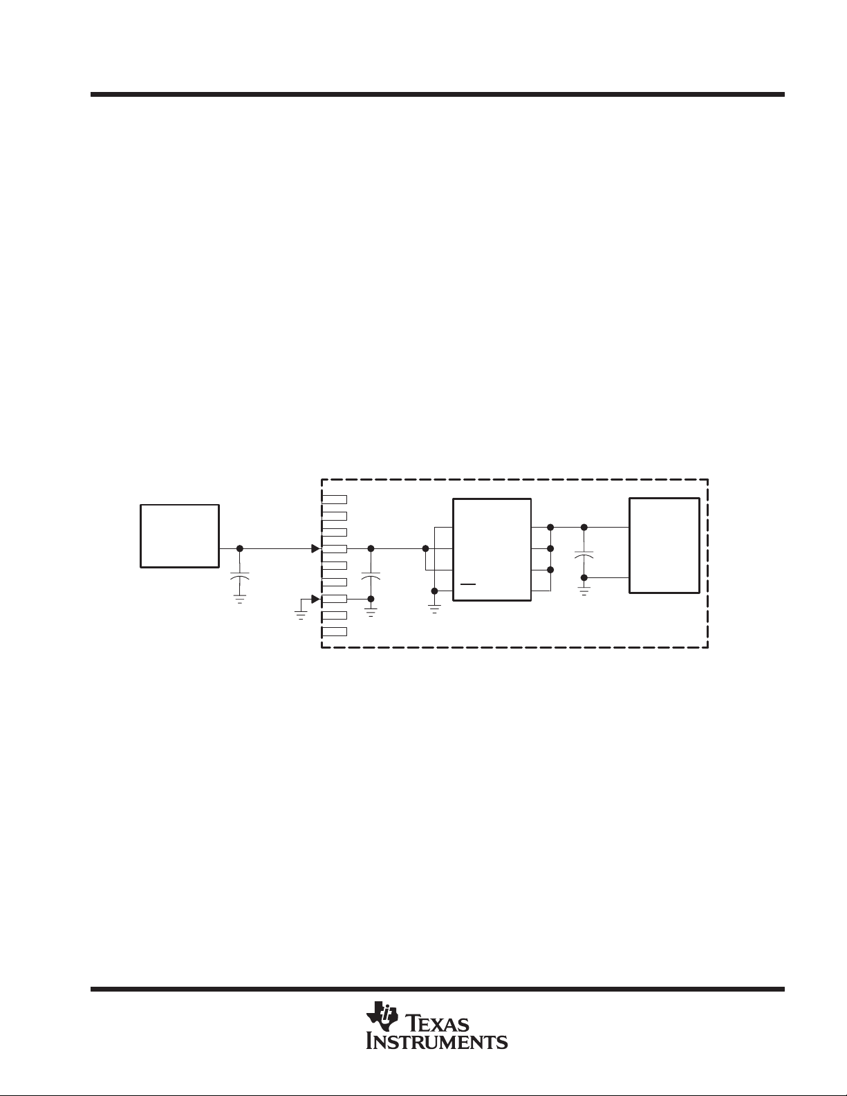
TPS201xA functional block diagram
°
ENABLE
LOAD CURRENT
(A)
0.2 0.3 TPS2010AD TPS2010APWPR
w
0.6 0.9 TPS2011AD TPS2011APWPR
1 1.5 TPS2012AD TPS2012APWPR
1.5 2.2 TPS2013AD TPS2013APWPR
Charge
Pump
TYPICAL SHORT-CIRCUIT
CURRENT LIMIT AT 25°C
(A)
Power Switch
SMALL OUTLINE
(D)
†
CS
PACKAGED DEVICES
†
OUTIN
TSSOP
(PWP)
‡
EN
GND
†
Current Sense
UVLO
Driver
Thermal
Sense
Terminal Functions
TERMINAL
NAME
EN 4 7 I Enable input. Logic low turns on power switch.
GND 1 1 I Ground
IN 2, 3 2–6 I Input voltage
OUT 5, 6, 7, 8 8–14 O Power-switch output
NO.
D
NO.
PWP
I/O DESCRIPTION
Current
Limit
2
POST OFFICE BOX 655303 • DALLAS, TEXAS 75265

detailed description
power switch
TPS2010A, TPS2011A, TPS2012A, TPS2013A
POWER-DISTRIBUTION SWITCHES
SLVS189A – DECEMBER 1998 – REVISED NOVEMBER 1999
The power switch is an N-channel MOSFET with a maximum on-state resistance of 50 mΩ (V
Configured as a high-side switch, the power switch prevents current flow from OUT to IN and IN to OUT when
disabled.
charge pump
An internal charge pump supplies power to the driver circuit and provides the necessary voltage to pull the gate
of the MOSFET above the source. The charge pump operates from input voltages as low as 2.7 V and requires
very little supply current.
driver
The driver controls the gate voltage of the power switch. T o limit large current surges and reduce the associated
electromagnetic interference (EMI) produced, the driver incorporates circuitry that controls the rise times and
fall times of the output voltage. The rise and fall times are typically in the 2-ms to 9-ms range.
enable (EN
current sense
)
The logic enable disables the power switch, the bias for the charge pump, driver, and other circuitry to reduce
the supply current to less than 10 µA when a logic high is present on EN . A logic zero input on EN restores bias
to the drive and control circuits and turns the power on. The enable input is compatible with both TTL and CMOS
logic levels.
A sense FET monitors the current supplied to the load. The sense FET measures current more efficiently than
conventional resistance methods. When an overload or short circuit is encountered, the current-sense circuitry
sends a control signal to the driver. The driver, in turn, reduces the gate voltage and drives the power FET into
its saturation region, which switches the output into a constant current mode and holds the current constant
while varying the voltage on the load.
I(IN)
= 5 V).
thermal sense
An internal thermal-sense circuit shuts off the power switch when the junction temperature rises to
approximately 140°C. Hysteresis is built into the thermal sense circuit. After the device has cooled
approximately 20°C, the switch turns back on. The switch continues to cycle off and on until the fault is removed.
undervoltage lockout
A voltage sense circuit monitors the input voltage. When the input voltage is below approximately 2 V , a control
signal turns off the power switch.
POST OFFICE BOX 655303 • DALLAS, TEXAS 75265
3
TPS2010A, TPS2011A, TPS2012A, TPS2013A
Input voltage
Continuous output current, I
A
POWER-DISTRIBUTION SWITCHES
SLVS189A – DECEMBER 1998 – REVISED NOVEMBER 1999
absolute maximum ratings over operating free-air temperature range (unless otherwise noted)
Input voltage range, V
Output voltage range, V
Input voltage range, V
Continuous output current, I
Continuous total power dissipation See Dissipation Rating Table. . . . . . . . . . . . . . . . . . . . . . . . . . . . . . . . . . . . . .
Operating virtual junction temperature range, T
Storage temperature range, T
Lead temperature soldering 1,6 mm (1/16 inch) from case for 10 seconds 260°C. . . . . . . . . . . . . . . . . . . . . . .
Electrostatic discharge (ESD) protection: Human body model 2 kV. . . . . . . . . . . . . . . . . . . . . . . . . . . . . . . . . . .
†
Stresses beyond those listed under “absolute maximum ratings” may cause permanent damage to the device. These are stress ratings only, and
functional operation of the device at these or any other conditions beyond those indicated under “recommended operating conditions” is not
implied. Exposure to absolute-maximum-rated conditions for extended periods may affect device reliability.
NOTE 1: All voltages are with respect to GND.
PACKAGE
D 725 mW 5.8 mW/°C 464 mW 377 mW
PWP 700 mW 5.6 mW/°C 448 mW 364 mW
(see Note 1) –0.3 V to 6 V. . . . . . . . . . . . . . . . . . . . . . . . . . . . . . . . . . . . . . . . . . . . . . . .
I(IN)
O(OUT)
(see Note 1) –0.3 V to V
I(EN)
O(OUT)
J
stg
Machine model 200V. . . . . . . . . . . . . . . . . . . . . . . . . . . . . . . . . . . . . .
DISSIPATION RATING TABLE
TA ≤ 25°C
POWER RATING
DERATING FACTOR
ABOVE TA = 25°C
TA = 70°C
POWER RATING
TA = 85°C
POWER RATING
+ 0.3 V. . . . . . . . . . . . . . . . . . . . . . . . . . . . . . . . . .
I(IN)
–0.3 V to 6 V. . . . . . . . . . . . . . . . . . . . . . . . . . . . . . . . . . . . . . . . . . . . . . . . . . . . . . . . . .
internally limited. . . . . . . . . . . . . . . . . . . . . . . . . . . . . . . . . . . . . . . . . . . . . . . . .
–40°C to 125°C. . . . . . . . . . . . . . . . . . . . . . . . . . . . . . . . . . . . . .
–65°C to 150°C. . . . . . . . . . . . . . . . . . . . . . . . . . . . . . . . . . . . . . . . . . . . . . . . . . . .
recommended operating conditions
MIN MAX UNIT
p
p
Operating virtual junction temperature, T
O
V
V
TPS2010A 0 0.2
TPS2011A 0 0.6
TPS2012A 0 1
TPS2013A 0 1.5
I(IN)
I(EN)
J
2.7 5.5 V
0 5.5 V
–40 125 °C
†
4
POST OFFICE BOX 655303 • DALLAS, TEXAS 75265
r
DS(on)
Static drain-source on-state resistance
mΩ
trRise time, output
ms
tfFall time, output
ms
VILLow-level in ut voltage
V
ms
IOSShort-circuit output current
OUT
GND
evice enable
A
Device enable into short circuit
TPS2010A, TPS2011A, TPS2012A, TPS2013A
POWER-DISTRIBUTION SWITCHES
SLVS189A – DECEMBER 1998 – REVISED NOVEMBER 1999
electrical characteristics over recommended operating junction temperature range, V
= rated current, EN = 0 V (unless otherwise noted)
I
O
I(IN)
= 5.5 V,
power switch
PARAMETER
V
I(IN)
V
I(IN)
V
I(IN)
V
I(IN)
V
I(IN)
V
I(IN)
V
I(IN)
V
I(IN)
V
I(IN)
V
I(IN)
V
I(IN)
V
I(IN)
V
I(IN)
p
p
†
Pulse-testing techniques maintain junction temperature close to ambient temperature; thermal effects must be taken into account separately.
CL = 1 µF,
V
I(IN)
CL = 1 µF,
V
I(IN)
CL = 1 µF,
V
I(IN)
CL = 1 µF,
TEST CONDITIONS
= 5 V, TJ = 25°C, IO = 1.5 A 33 36
= 5 V, TJ = 85°C, IO = 1.5 A 38 46
= 5 V, TJ = 125°C, IO = 1.5 A 44 50
= 3.3 V, TJ = 25°C, IO = 1.5 A 37 41
= 3.3 V, TJ = 85°C, IO = 1.5 A 43 52
= 3.3 V, TJ = 125°C, IO = 1.5 A 51 61
= 5 V, TJ = 25°C, IO = 0.18 A 30 34
= 5 V, TJ = 85°C, IO = 0.18 A 35 41
= 5 V, TJ = 125°C, IO = 0.18 A 39 47
= 3.3 V, TJ = 25°C, IO = 0.18 A 33 37
= 3.3 V, TJ = 85°C, IO = 0.18 A 39 46
= 3.3 V, TJ = 125°C, IO = 0.18 A 44 56
= 5.5 V,
= 2.7 V,
= 5.5 V,
= 2.7 V,
TJ = 25°C,
RL = 10 Ω
TJ = 25°C,
RL = 10 Ω
TJ = 25°C,
RL = 10 Ω
TJ = 25°C,
RL = 10 Ω
†
MIN TYP MAX UNIT
6.1
8.6
3.4
3
enable input (EN)
PARAMETER TEST CONDITIONS
V
t
t
High-level input voltage 2.7 V ≤ V
IH
p
I
Input current EN = 0 V or EN = V
I
Turnon time CL = 100 µF, RL = 10 Ω 20
on
Turnoff time CL = 100 µF, RL = 10 Ω 40
off
4.5 V ≤ V
2.7 V ≤ V
≤ 5.5 V 2 V
I(IN)
≤ 5.5 V 0.8
I(IN)
≤ 4.5 V 0.5
I(IN)
I(IN)
MIN TYP MAX UNIT
–0.5 0.5 µA
current limit
PARAMETER
p
†
Pulse-testing techniques maintain junction temperature close to ambient temperature; thermal effects must be taken into account separately.
TJ = 25°C, VI = 5.5 V,
connected to
D
TEST CONDITIONS
,
into short circuit
†
TPS2010A 0.22 0.3 0.4
TPS201 1A 0.66 0.9 1.1
TPS2012A 1.1 1.5 1.8
TPS2013A 1.65 2.2 2.7
MIN TYP MAX UNIT
POST OFFICE BOX 655303 • DALLAS, TEXAS 75265
5
TPS2010A, TPS2011A, TPS2012A, TPS2013A
Supply current, low-level output
No Load on OUT
A
Supply current, high-level output
No Load on OUT
EN
V
A
POWER-DISTRIBUTION SWITCHES
SLVS189A – DECEMBER 1998 – REVISED NOVEMBER 1999
electrical characteristics over recommended operating junction temperature range, V
= rated current, EN = 0 V (unless otherwise noted) (continued)
I
O
I(IN)
= 5.5 V,
supply current
PARAMETER TEST CONDITIONS MIN TYP MAX UNIT
pp
pp
Leakage current OUT connected to ground EN = V
p
p
EN = V
= 0
TJ = 25°C 0.3 1
I(IN)
–40°C ≤ TJ ≤ 125°C 10
TJ = 25°C 58 75
–40°C ≤ TJ ≤ 125°C 75 100
–40°C ≤ TJ ≤ 125°C 10 µA
I(IN)
undervoltage lockout
PARAMETER TEST CONDITIONS MIN TYP MAX UNIT
Low-level input voltage 2 2.5 V
Hysteresis TJ = 25°C 100 mV
µ
µ
6
POST OFFICE BOX 655303 • DALLAS, TEXAS 75265
TPS2010A, TPS2011A, TPS2012A, TPS2013A
POWER-DISTRIBUTION SWITCHES
SLVS189A – DECEMBER 1998 – REVISED NOVEMBER 1999
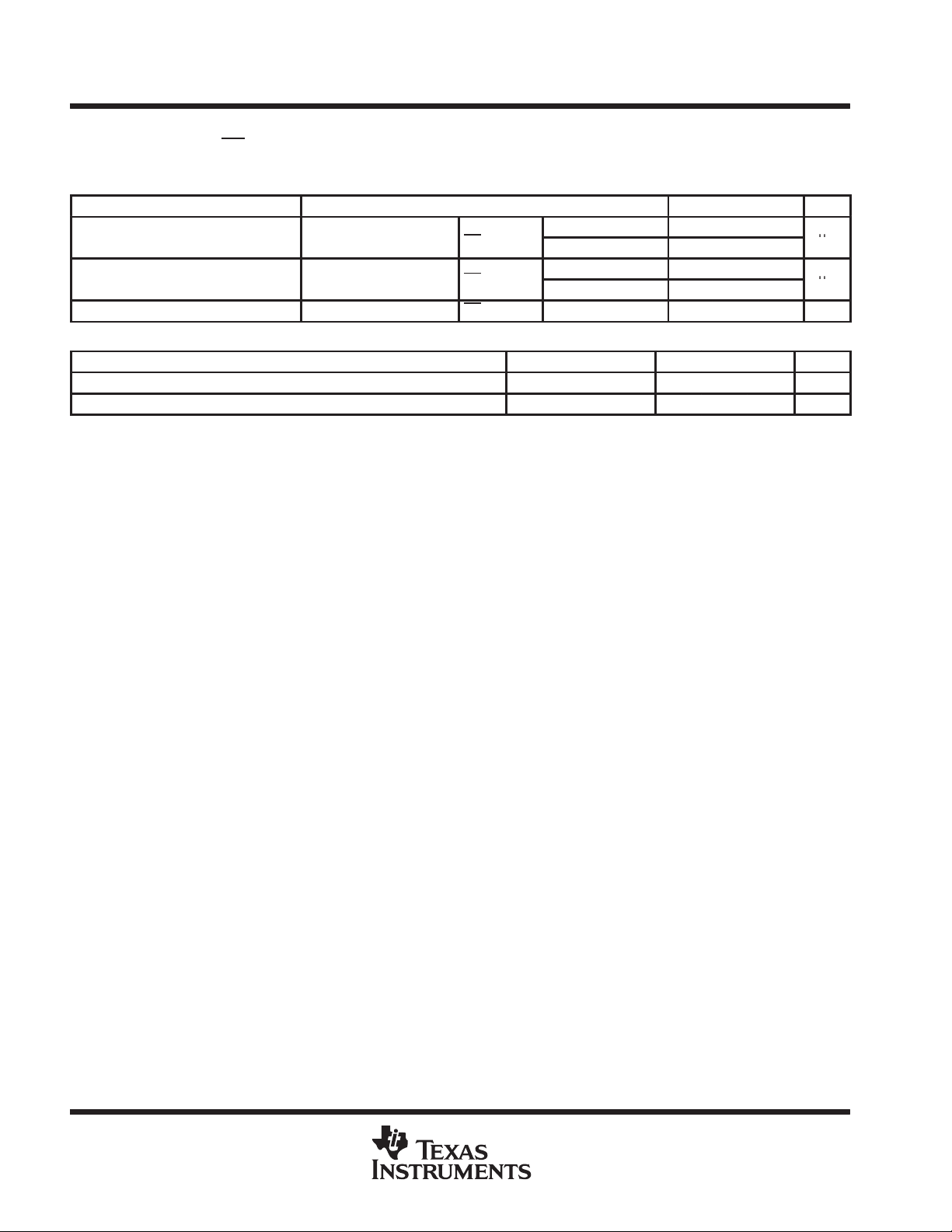
PARAMETER MEASUREMENT INFORMATION
OUT
RL CL
TEST CIRCUIT
V
V
O(OUT)
I(EN)
50%
t
on
VOLTAGE WAVEFORMS
50%
90%
V
10%
O(OUT)
t
r
90%
90%
10%
t
off
10%
t
f
Figure 1. Test Circuit and Voltage Waveforms
Table of Timing Diagrams
FIGURE
Turnon Delay and Rise TIme 2
Turnoff Delay and Fall Time 3
Turnon Delay and Rise TIme with 1-µF Load 4
Turnoff Delay and Rise TIme with 1-µF Load 5
Device Enabled into Short 6
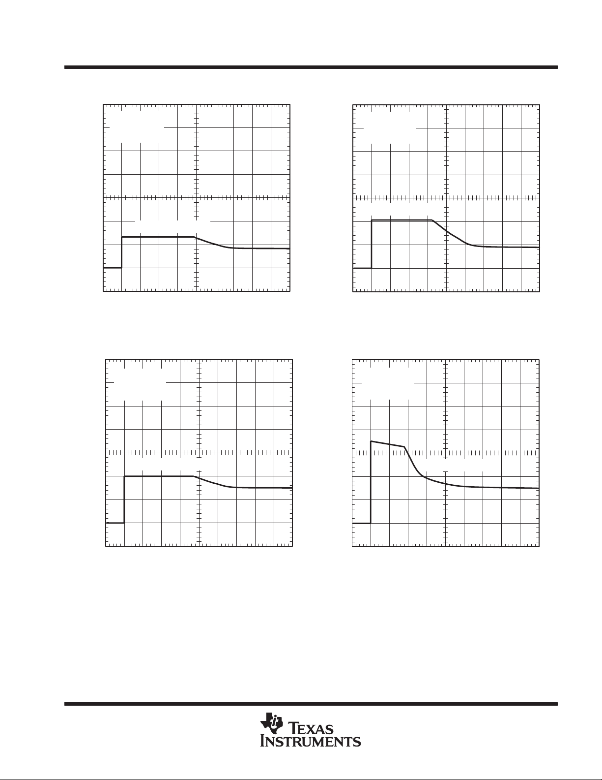
TPS2010A, TPS201 1A, TPS2012A, and TPS2013A, Ramped Load on Enabled Device 7, 8, 9, 10
TPS2013A, Inrush Current 11
7.9-Ω Load Connected to an Enabled TPS2010A Device 12
3.7-Ω Load Connected to an Enabled TPS2010A Device 13
3.7-Ω Load Connected to an Enabled TPS2011A Device 14
2.6-Ω Load Connected to an Enabled TPS2011A Device 15
2.6-Ω Load Connected to an Enabled TPS2012A Device 16
1.2-Ω Load Connected to an Enabled TPS2012A Device 17
1.2-Ω Load Connected to an Enabled TPS2013A Device 18
0.9-Ω Load Connected to an Enabled TPS2013A Device 19
POST OFFICE BOX 655303 • DALLAS, TEXAS 75265
7
TPS2010A, TPS2011A, TPS2012A, TPS2013A
POWER-DISTRIBUTION SWITCHES
SLVS189A – DECEMBER 1998 – REVISED NOVEMBER 1999
PARAMETER MEASUREMENT INFORMATION
V
(5 V/div)
V
I(EN)
I(EN)
V
I(EN)
V
I(EN)
(5 V/div)
V
= 5 V
I(IN)
RL = 27 Ω
TA = 25°C
V
O(OUT)
V
I(EN)
O(OUT)
V
2
0
468101214161820
t – Time – ms
O(OUT)
(2 V/div)
VIN = 5 V
RL = 27 Ω
TA = 25°C
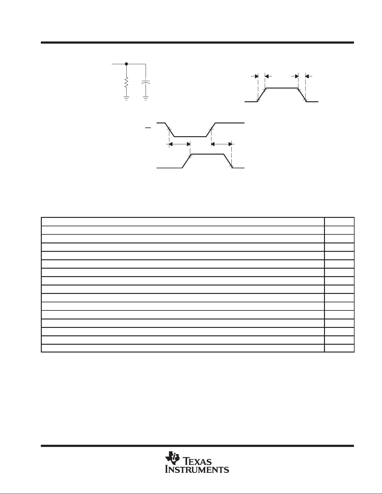
Figure 2. Turnon Delay and Rise Time
V
(5 V/div)
I(EN)
V
O(OUT)
(2 V/div)
V
I(IN)
CL = 1 µF
RL = 27 Ω
TA = 25°C
= 5 V
V
O(OUT)
V
V
O(OUT)
V
2 4 6 8 10 12 14 16 18 20
0
O(OUT)
t – Time – ms
(2 V/div)
Figure 3. Turnoff Delay and Fall Time
V
(5 V/div)
I(EN)
I(EN)
V
= 5 V
I(IN)
CL = 1 µF
RL = 27 Ω
TA = 25°C
V
O(OUT)
(2 V/div)
2
2
0
4 6 81012141618 20
t – Time – ms
Figure 4. Turnon Delay and Rise Time
0
Figure 5. Turnoff Delay and Fall Time
With 1-µF Load
8
POST OFFICE BOX 655303 • DALLAS, TEXAS 75265
468101214161820
t – Time – ms
With 1-µF Load

V
I(EN)
I
O(OUT)
PARAMETER MEASUREMENT INFORMATION
V
(5 V/div)
I(EN)
V
= 5 V
I(IN)
TA = 25°C
TPS2013A
TPS2012A
TPS2011A
TPS2010A
I
0
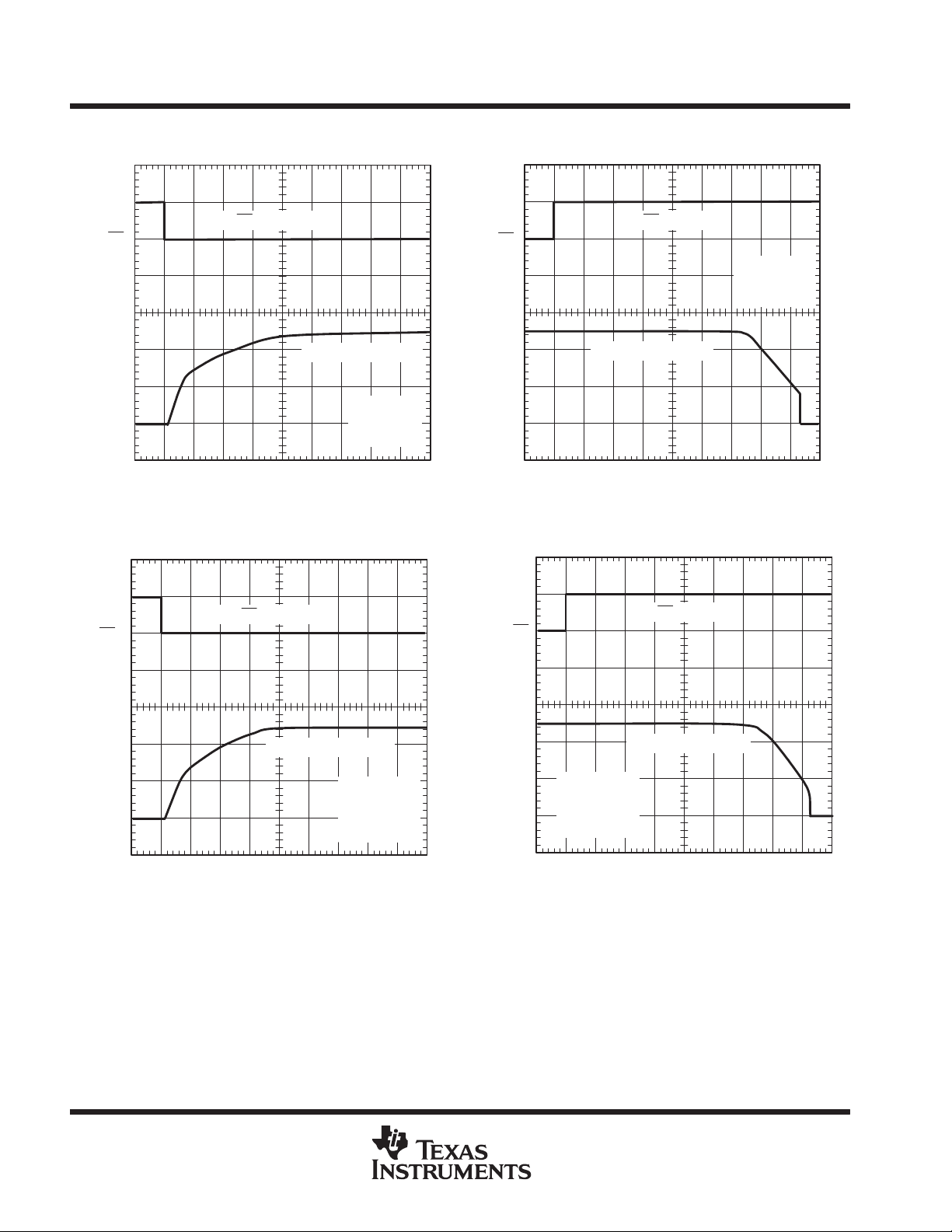
Figure 6. Device Enabled Into Short
(1 A/div)
O(OUT)
1
2345678910
t – Time – ms
TPS2010A, TPS2011A, TPS2012A, TPS2013A
POWER-DISTRIBUTION SWITCHES
SLVS189A – DECEMBER 1998 – REVISED NOVEMBER 1999
V
= 5 V
I(IN)
TA = 25°C
I
O(OUT)
I
20 40 60 80 100 120 140 160 180 200
0
t – Time – ms
Figure 7. TPS2010A, Ramped Load on
Enabled Device
O(OUT)
(500 mA/div)
V
= 5 V
I(IN)
TA = 25°C
I
O(OUT)
I
20 40 60 80 100 120 140 160 180 200
0
O(OUT)
(1 A/div)
t – Time – ms
Figure 8. TPS2011A, Ramped Load on Enabled
Device
I
O(OUT)
V
= 5 V
I(IN)
TA = 25°C
I
20 40 60 80 100 120 140 160 180 200
0
O(OUT)
(1 A/div)
t – Time – ms
Figure 9. TPS2012A, Ramped Load on
Enabled Device
POST OFFICE BOX 655303 • DALLAS, TEXAS 75265
9
TPS2010A, TPS2011A, TPS2012A, TPS2013A
POWER-DISTRIBUTION SWITCHES
SLVS189A – DECEMBER 1998 – REVISED NOVEMBER 1999
PARAMETER MEASUREMENT INFORMATION
V
= 5 V
I(IN)
TA = 25°C
V
I(EN)
V
I(EN)
(5 V/div)
470 µF
O(OUT)
I
20 40 60 80 100 120 140 160 180 200
0
O(OUT)
(1 A/div)
t – Time – ms
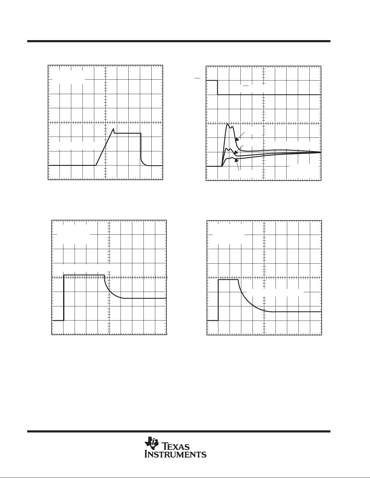
Figure 10. TPS2013A, Ramped Load on
Enabled Device
V
= 5 V
I(IN)
RL = 7.9 Ω
TA = 25°C
I
O(OUT)
(200 mA/div)
I
I(IN)
150 µF
47 µF
123 4567 8910
0
t – Time – ms
I
I(IN)
Figure 11. TPS2013A, Inrush Current
V
= 5 V
I(IN)
RL = 3.7 Ω
TA = 25°C
I
O(OUT)
(500 mA/div)
(500 mA/div)
RL = 10 Ω
TA = 25°C
I
O(OUT)
200 400 600 800 1000 12001400 1600 1800 2000
0
t – Time – µs
Figure 12. 7.9-Ω Load Connected to an Enabled
TPS2010A Device
10
POST OFFICE BOX 655303 • DALLAS, TEXAS 75265
I
O(OUT)
50 100 150 200 250 300 350 400 450 500
0
t – Time – µs
Figure 13. 3.7-Ω Load Connected to an Enabled
TPS2010A Device
TPS2010A, TPS2011A, TPS2012A, TPS2013A
POWER-DISTRIBUTION SWITCHES
SLVS189A – DECEMBER 1998 – REVISED NOVEMBER 1999
PARAMETER MEASUREMENT INFORMATION
V
= 5 V
I(IN)
RL = 3.7 Ω
TA = 25°C
V
= 5 V
I(IN)
RL = 2.6 Ω
TA = 25°C
I
O(OUT)
I
200 400 600 800 1000 1200 1400 1600 1800 2000
0
O(OUT)
(1 A/div)
t – Time – µs
Figure 14. 3.7-Ω Load Connected to an Enabled
TPS2011A Device
V
= 5 V
I(IN)
RL = 2.6 Ω
TA = 25°C
I
O(OUT)
(1 A/div)
I
O(OUT)
I
50 100 150 200 250 300 350 400 450 500
0
O(OUT)
(1 A/div)
t – Time – µs
Figure 15. 2.6-Ω Load Connected to an Enabled
TPS2011A Device
V
= 5 V
I(IN)
RL = 1.2 Ω
TA = 25°C
I
O(OUT)
(1 A/div)
I
O(OUT)
200 400 600 800 1000 12001400 1600 1800 2000
0
t – Time – µs
Figure 16. 2.6-Ω Load Connected to an Enabled
TPS2012A Device
POST OFFICE BOX 655303 • DALLAS, TEXAS 75265
I
O(OUT)
100 200 300 400 500 600 700 800 900 1000
0
t – Time – µs
Figure 17. 1.2-Ω Load Connected to an Enabled
TPS2012A Device
11

TPS2010A, TPS2011A, TPS2012A, TPS2013A
POWER-DISTRIBUTION SWITCHES
SLVS189A – DECEMBER 1998 – REVISED NOVEMBER 1999
PARAMETER MEASUREMENT INFORMATION
V
= 5 V
I(IN)
RL = 1.2 Ω
TA = 25°C
I
O(OUT)
I
100 200 300 400 500 600 700 800 900 1000
0
O(OUT)
(2 A/div)
t – Time – µs
Figure 18. 1.2-Ω Load Connected to an Enabled
TPS2013A Device
V
= 5 V
I(IN)
RL = 0.9 Ω
TA = 25°C
I
O(OUT)
(2 A/div)
12
I
O(OUT)
100 200 300 400 500 600 700 800 900 1000
0
t – Time – µs
Figure 19. 0.9-Ω Load Connected to an Enabled
TPS2013A Device
POST OFFICE BOX 655303 • DALLAS, TEXAS 75265

IOSShort-circuit current limit
r
Static drain-source on-state resistance
TPS2010A, TPS2011A, TPS2012A, TPS2013A
POWER-DISTRIBUTION SWITCHES
SLVS189A – DECEMBER 1998 – REVISED NOVEMBER 1999
TYPICAL CHARACTERISTICS
Table of Graphs
FIGURE
t
d(on)
t
d(off)
t
r
t
f
DS(on)
V
I
Turnon delay time vs Output voltage 20
Turnoff delay time vs Input voltage 21
Rise time vs Load current 22
Fall time vs Load current 23
Supply current (enabled) vs Junction temperature 24
Supply current (disabled) vs Junction temperature 25
Supply current (enabled) vs Input voltage 26
Supply current (disabled) vs Input voltage 27
vs Input voltage 28
vs Junction temperature 29
vs Input voltage 30
vs Junction temperature 31
vs Input voltage 32
vs Junction temperature 33
Input voltage Undervoltage lockout 34
TURNON DELAY TIME
7.5
7
6.5
6
5.5
5
– Turn-on Delay T ime – ms
4.5
d(on)
t
4
3.5
2.5 3 3.5 4 4.5
vs
OUTPUT VOLTAGE
TA = 25°C
CL = 1 µF
VI – Input Voltage – V
Figure 20
5 5.5 6
TURNOFF DELAY TIME
18
TA = 25°C
CL = 1 µF
17.5
17
– Turn-off Delay T ime – ms
16.5
d(off)
t
16
2.5 3 3.5 4 4.5
vs
INPUT VOLTAGE
5 5.5 6
VI – Input Voltage – V
Figure 21
POST OFFICE BOX 655303 • DALLAS, TEXAS 75265
13

TPS2010A, TPS2011A, TPS2012A, TPS2013A
POWER-DISTRIBUTION SWITCHES
SLVS189A – DECEMBER 1998 – REVISED NOVEMBER 1999
TYPICAL CHARACTERISTICS
6.5
6
– Rise Time – ms
5.5
r
t
5
75
65
RISE TIME
LOAD CURRENT
TA = 25°C
CL = 1 µF
0 0.5 1
IL – Load Current – A
Figure 22
SUPPLY CURRENT (ENABLED)
JUNCTION TEMPERATURE
V
= 5.5 V
I(IN)
V
= 5 V
I(IN)
vs
vs
1.5 2
3.5
3.25
3
– Fall Time – ms
f
t
2.75
2.5
5
4
3
FALL TIME
vs
LOAD CURRENT
TA = 25°C
CL = 1 µF
0 0.5
IL – Load Current – A
1 1.5 2
Figure 23
SUPPLY CURRENT (DISABLED)
vs
JUNCTION TEMPERATURE
V
I(IN)
V
I(IN)
= 5.5 V
= 5 V
14
55
45
Supply Current (Enabled) – Aµ
35
–50 –25 0 25 50
TJ – Junction Temperature – °C
Figure 24
V
= 4 V
I(IN)
V
= 3.3 V
I(IN)
V
= 2.7 V
I(IN)
75 100 150
POST OFFICE BOX 655303 • DALLAS, TEXAS 75265
125
Supply Current (Disabled) – Aµ
2
1
0
–1
–50 –25 0 25 50
TJ – Junction Temperature – °C
Figure 25
V
= 4 V
I(IN)
V
= 3.3 V
I(IN)
V
= 2.7 V
I(IN)
75 100 150
125

TPS2010A, TPS2011A, TPS2012A, TPS2013A
POWER-DISTRIBUTION SWITCHES
SLVS189A – DECEMBER 1998 – REVISED NOVEMBER 1999
TYPICAL CHARACTERISTICS
SUPPLY CURRENT (ENABLED)
75
TJ = 125°C
TJ = 85°C
65
55
45
Supply Current (Enabled) – Aµ
35
2.5 3 3.5 4 4.5
SHORT-CIRCUIT CURRENT LIMIT
3.5
TA = 25°C
3
vs
INPUT VOLTAGE
TJ = 0°C
TJ = –40°C
VI – Input Voltage – V
Figure 26
vs
INPUT VOLTAGE
TJ = 25°C
5 5.5 6
SUPPLY CURRENT (DISABLED)
5
4
3
2
1
Supply Current (Disabled) – Aµ
0
–1
TJ = 125°C
2.5 3 3.5 4 4.5
SHORT-CIRCUIT CURRENT LIMIT
JUNCTION TEMPERATURE
3.5
3
vs
INPUT VOLTAGE
TJ = 85°C
TJ = 25°C
TJ = 0°C
TJ = –40°C
5 5.5 6
VI – Input Voltage – V
Figure 27
vs
– Short-Circuit Current Limit – A
I
2.5
2
1.5
1
OS
0.5
0
23 4
VI – Input Voltage – V
Figure 28
TPS2013A
TPS2012A
TPS2011A
TPS2010A
2.5
2
1.5
1
– Short-Circuit Current Limit – A
OS
I
0.5
0
56
POST OFFICE BOX 655303 • DALLAS, TEXAS 75265
–50 –25 0
TPS2013A
TPS2012A
TPS2011A
TPS2010A
25 100
TJ – Junction Temperature – °C
50 75
Figure 29
15

TPS2010A, TPS2011A, TPS2012A, TPS2013A
POWER-DISTRIBUTION SWITCHES
SLVS189A – DECEMBER 1998 – REVISED NOVEMBER 1999
TYPICAL CHARACTERISTICS
STATIC DRAIN-SOURCE ON-STATE RESISTANCE
vs
Ω
60
50
40
30
– Static Drain-Source On-State Resistance – m
20
2.5 3 3.5
DS(on)
r
INPUT VOLTAGE
IO = 0.18 A
TJ = 125°C
TJ = 25°C
TJ = –40°C
46
4.5 5
VI – Input Voltage – V
5.5
Figure 30
STATIC DRAIN-SOURCE ON-STATE RESISTANCE
Ω
60
IO = 1.5 A
INPUT VOLTAGE
vs
STATIC DRAIN-SOURCE ON-STATE RESISTANCE
Ω
60
50
40
30
– Static Drain-Source On-State Resistance – m
20
DS(on)
–50 –25 0
r
JUNCTION TEMPERATURE
IO = 0.18 A
VI = 2.7 V
VI = 3.3 V
TJ – Junction Temperature – °C
vs
VI = 5.5 V
50 75 100
25 150
125
Figure 31
STATIC DRAIN-SOURCE ON-STATE RESISTANCE
Ω
60
JUNCTION TEMPERATURE
IO = 1.5 A
vs
50
40
TJ = 25°C
30
– Static Drain-Source On-State Resistance – m
20
DS(on)
r
3 3.5
46
VI – Input Voltage – V
TJ = –40°C
4.5 5 5.5
Figure 32
16
TJ = 125°C
– Static Drain-Source On-State Resistance – m
DS(on)
r
POST OFFICE BOX 655303 • DALLAS, TEXAS 75265
50
40
30
20
–50 –25 0
VI = 3.3 V
VI = 4 V
VI = 5.5 V
25 150
50 75 100
TJ – Junction Temperature – °C
Figure 33
125

TPS2010A, TPS2011A, TPS2012A, TPS2013A
POWER-DISTRIBUTION SWITCHES
SLVS189A – DECEMBER 1998 – REVISED NOVEMBER 1999
TYPICAL CHARACTERISTICS
UNDERVOLTAGE LOCKOUT
2.5
2.4
Start Threshold
2.3
Power Supply
2.7 V to 5.5 V
2.2
– Input Voltage – V
I
V
2.1
2
–50 0 50 100
Stop Threshold
TJ – Temperature – °C
Figure 34
APPLICATION INFORMATION
2,3
IN
0.1 µF
4
EN
TPS2013A
GND
1
OUT
5,6,7,8
0.1 µF 22 µF
150
Load
Figure 35. Typical Application
power-supply considerations
A 0.01-µF to 0.1-µF ceramic bypass capacitor between IN and GND, close to the device, is recommended.
Placing a high-value electrolytic capacitor on the output and input pins is recommended when the output load
is heavy. This precaution reduces power supply transients that may cause ringing on the input. Additionally,
bypassing the output with a 0.01-µF to 0.1-µF ceramic capacitor improves the immunity of the device to
short-circuit transients.
overcurrent
A sense FET checks for overcurrent conditions. Unlike current-sense resistors, sense FET s do not increase the
series resistance of the current path. When an overcurrent condition is detected, the device maintains a
constant output current and reduces the output voltage accordingly . Complete shutdown occurs only if the fault
is present long enough to activate thermal limiting.
POST OFFICE BOX 655303 • DALLAS, TEXAS 75265
17

TPS2010A, TPS2011A, TPS2012A, TPS2013A
POWER-DISTRIBUTION SWITCHES
SLVS189A – DECEMBER 1998 – REVISED NOVEMBER 1999
APPLICATION INFORMATION
overcurrent (continued)
Three possible overload conditions can occur. In the first condition, the output has been shorted before the
device is enabled or before V
immediately switches into a constant-current output.
In the second condition, the excessive load occurs while the device is enabled. At the instant the excessive load
occurs, very high currents may flow for a short time before the current-limit circuit can react (see Figures 12–19).
After the current-limit circuit has tripped (reached the overcurrent trip threshhold) the device switches into
constant-current mode.
In the third condition, the load has been gradually increased beyond the recommended operating current. The
current is permitted to rise until the current-limit threshold is reached or until the thermal limit of the device is
exceeded (see Figures 7–10). The TPS201xA is capable of delivering current up to the current-limit threshold
without damaging the device. Once the threshold has been reached, the device switches into its
constant-current mode.
power dissipation and junction temperature
has been applied (see Figure 6). The TPS201xA senses the short and
I(IN)
The low on-resistance on the n-channel MOSFET allows small surface-mount packages, such as SOIC, to pass
large currents. The thermal resistances of these packages are high compared to those of power packages; it
is good design practice to check power dissipation and junction temperature. The first step is to find r
the input voltage and operating temperature. As an initial estimate, use the highest operating ambient
temperature of interest and read r
P
+
r
D
DS(on
Finally, calculate the junction temperature:
T
+
P
J
Where:
Compare the calculated junction temperature with the initial estimate. If they do not agree within a few degrees,
repeat the calculation, using the calculated value as the new estimate. Two or three iterations are generally
sufficient to get an acceptable answer.
D
TA = Ambient Temperature °C
R
= Thermal resistance SOIC = 172°C/W
θJA
2
I
)
R
)
JA
T
A
q
from Figures 30–33. Next, calculate the power dissipation using:
DS(on)
thermal protection
Thermal protection prevents damage to the IC when heavy-overload or short-circuit faults are present for
extended periods of time. The faults force the TPS201xA into constant current mode, which causes the voltage
across the high-side switch to increase; under short-circuit conditions, the voltage across the switch is equal
to the input voltage. The increased dissipation causes the junction temperature to rise to high levels. The
protection circuit senses the junction temperature of the switch and shuts it off. Hysteresis is built into the thermal
sense circuit, and after the device has cooled approximately 20 degrees, the switch turns back on. The switch
continues to cycle in this manner until the load fault or input power is removed.
DS(on)
at
18
POST OFFICE BOX 655303 • DALLAS, TEXAS 75265
TPS2010A, TPS2011A, TPS2012A, TPS2013A
POWER-DISTRIBUTION SWITCHES
SLVS189A – DECEMBER 1998 – REVISED NOVEMBER 1999
APPLICATION INFORMATION
undervoltage lockout (UVLO)
An undervoltage lockout ensures that the power switch is in the off state at power up. Whenever the input voltage
falls below approximately 2 V, the power switch will be quickly turned off. This facilitates the design of
hot-insertion systems where it is not possible to turn off the power switch before input power is removed. The
UVLO will also keep the switch from being turned on until the power supply has reached at least 2 V, even if
the switch is enabled. Upon reinsertion, the power switch will be turned on, with a controlled rise time to reduce
EMI and voltage overshoots.
generic hot-plug applications (see Figure 36)
In many applications it may be necessary to remove modules or pc boards while the main unit is still operating.
These are considered hot-plug applications. Such implementations require the control of current surges seen
by the main power supply and the card being inserted. The most effective way to control these surges is to limit
and slowly ramp the current and voltage being applied to the card, similar to the way in which a power supply
normally turns on. Because of the controlled rise times and fall times of the TPS201xA series, these devices
can be used to provide a softer start-up to devices being hot-plugged into a powered system. The UVLO feature
of the TPS201xA also ensures the switch will be off after the card has been removed, and the switch will be off
during the next insertion. The UVLO feature guarantees a soft start with a controlled rise time for every insertion
of the card or module.
PC Board
Power
Supply
2.7 V to 5.5 V
1000 µF
Optimum
0.1 µF
TPS2013A
GND
IN
IN
EN
OUT
OUT
OUT
OUT
Block of
Circuitry
Figure 36. Typical Hot-Plug Implementation
By placing the TPS201xA between the VCC input and the rest of the circuitry, the input power will reach this
device first after insertion. The typical rise time of the switch is approximately 9 ms, providing a slow voltage
ramp at the output of the device. This implementation controls system surge currents and provides a
hot-plugging mechanism for any device.
POST OFFICE BOX 655303 • DALLAS, TEXAS 75265
19

TPS2010A, TPS2011A, TPS2012A, TPS2013A
POWER-DISTRIBUTION SWITCHES
SLVS189A – DECEMBER 1998 – REVISED NOVEMBER 1999
MECHANICAL DATA
D (R-PDSO-G**) PLASTIC SMALL-OUTLINE PACKAGE
14 PIN SHOWN
0.050 (1,27)
14
1
0.069 (1,75) MAX
0.020 (0,51)
0.014 (0,35)
8
7
A
0.010 (0,25)
0.004 (0,10)
DIM
0.157 (4,00)
0.150 (3,81)
PINS **
0.010 (0,25)
0.244 (6,20)
0.228 (5,80)
8
M
Seating Plane
0.004 (0,10)
14
0.008 (0,20) NOM
0°–8°
16
Gage Plane
0.010 (0,25)
0.044 (1,12)
0.016 (0,40)
A MAX
A MIN
NOTES: A. All linear dimensions are in inches (millimeters).
20
B. This drawing is subject to change without notice.
C. Body dimensions do not include mold flash or protrusion, not to exceed 0.006 (0,15).
D. Falls within JEDEC MS-012
POST OFFICE BOX 655303 • DALLAS, TEXAS 75265
0.197
(5,00)
0.189
(4,80)
0.344
(8,75)
0.337
(8,55)
0.394
(10,00)
0.386
(9,80)
4040047/D 10/96

TPS2010A, TPS2011A, TPS2012A, TPS2013A
POWER-DISTRIBUTION SWITCHES
SLVS189A – DECEMBER 1998 – REVISED NOVEMBER 1999
MECHANICAL DATA
PWP (R-PDSO-G**) PowerPAD PLASTIC SMALL-OUTLINE P ACKAGE
20-PIN SHOWN
0,65
20
1
1,20 MAX
0,30
0,19
11
4,50
4,30
10
A
0,15
0,05
PINS **
DIM
M
0,10
6,60
6,20
Seating Plane
0,10
1614
Thermal Pad
(See Note D)
20
0,15 NOM
0°–8°
Gage Plane
0,25
0,75
0,50
2824
A MAX
A MIN
NOTES: A. All linear dimensions are in millimeters.
B. This drawing is subject to change without notice.
C. Body dimensions do not include mold flash or protrusions.
D. The package thermal performance may be enhanced by bonding the thermal pad to an external thermal plane. This pad is electrically
and thermally connected to the backside of the die and possibly selected leads.
E. Falls within JEDEC MO-153
PowerPAD is a trademark of Texas Instruments Incorporated.
5,10
4,90
5,10
4,90
6,60
6,40
7,90
7,70
9,80
9,60
4073225/E 03/97
POST OFFICE BOX 655303 • DALLAS, TEXAS 75265
21

IMPORTANT NOTICE
T exas Instruments and its subsidiaries (TI) reserve the right to make changes to their products or to discontinue
any product or service without notice, and advise customers to obtain the latest version of relevant information
to verify, before placing orders, that information being relied on is current and complete. All products are sold
subject to the terms and conditions of sale supplied at the time of order acknowledgement, including those
pertaining to warranty, patent infringement, and limitation of liability.
TI warrants performance of its semiconductor products to the specifications applicable at the time of sale in
accordance with TI’s standard warranty. Testing and other quality control techniques are utilized to the extent
TI deems necessary to support this warranty . Specific testing of all parameters of each device is not necessarily
performed, except those mandated by government requirements.
CERTAIN APPLICATIONS USING SEMICONDUCTOR PRODUCTS MAY INVOLVE POTENTIAL RISKS OF
DEATH, PERSONAL INJURY, OR SEVERE PROPERTY OR ENVIRONMENTAL DAMAGE (“CRITICAL
APPLICATIONS”). TI SEMICONDUCTOR PRODUCTS ARE NOT DESIGNED, AUTHORIZED, OR
WARRANTED TO BE SUITABLE FOR USE IN LIFE-SUPPORT DEVICES OR SYSTEMS OR OTHER
CRITICAL APPLICA TIONS. INCLUSION OF TI PRODUCTS IN SUCH APPLICATIONS IS UNDERST OOD TO
BE FULLY AT THE CUSTOMER’S RISK.
In order to minimize risks associated with the customer’s applications, adequate design and operating
safeguards must be provided by the customer to minimize inherent or procedural hazards.
TI assumes no liability for applications assistance or customer product design. TI does not warrant or represent
that any license, either express or implied, is granted under any patent right, copyright, mask work right, or other
intellectual property right of TI covering or relating to any combination, machine, or process in which such
semiconductor products or services might be or are used. TI’s publication of information regarding any third
party’s products or services does not constitute TI’s approval, warranty or endorsement thereof.
Copyright 1999, Texas Instruments Incorporated
 Loading...