

Page 1
User's Guide
SLRU005–February 2013
TPL7407L7-Channel Relay and Inductive Load Sink Driver
EVM
1 Overview
The TPL7407LEVM is a 7-Channel Relay and Inductive Load Sink Driver evaluation module that
demonstrates the TPL7407LDR integrated circuit from Texas Instruments (TI).
The TPL7407LDR is a high-performance peripheral driver designed to drive loads of many types
including: relays, stepper motors, lamps, and light emitting diodes.
The EVM is configured with seven push buttons that supply input to the TPL7407L driver and seven
relays are driven by the TPL7407Loutputs. A four terminal block can be connected to external power
supplies to provide input and relay power. All of the TPL7407Linput and output pins are accessible for
external connection.
1.1 TPL7407LEVM Features
• Seven numbered push buttons control input for device testing.
• Seven numbered light emitting diodes indicate relay contact closure.
• Three 0.1” spaced post connector ports that allow access to all input pins, output pins, and relay
contacts.
• Three open locations, per channel, on the circuit board for user supplied components.
• Onboard relay loads that can be disconnected by removing surface mounted 0Ω resistors.
• A large device clearance area that allows the use of small profile temperature forcing equipment.
Table 1. TPL7407LEVM Specification
Key Parameters
Input Supply Voltage: 0V – 5.5V
Relay Supply Voltage: 8.5V – 24V
Output Current: 0mA to 500mA
Number of Channels: 7
Onboard Load: Seven OMRON G5NB relays
G5NB specs
• Nominal coil resistance is 2,880Ω
• Nominal coil current is 8.3mA
• Nominal coil voltage is 24V
• Pickup voltage < 75% Nominal
• Dropout voltage > 10% Nominal
• Maximum coil voltage 180% Nominal
CAUTION: Applying voltages above the limitations given in Table 1 may cause permanent damage to
your hardware.
Gerber (layout) files are available at www.ti.com.
The EVM includes mating connectors for input, output, and contact pins.
SLRU005–February 2013 TPL7407L7-Channel Relay and Inductive Load Sink Driver EVM
Submit Documentation Feedback
1
Copyright © 2013, Texas Instruments Incorporated
Page 2
Quick Setup Guide
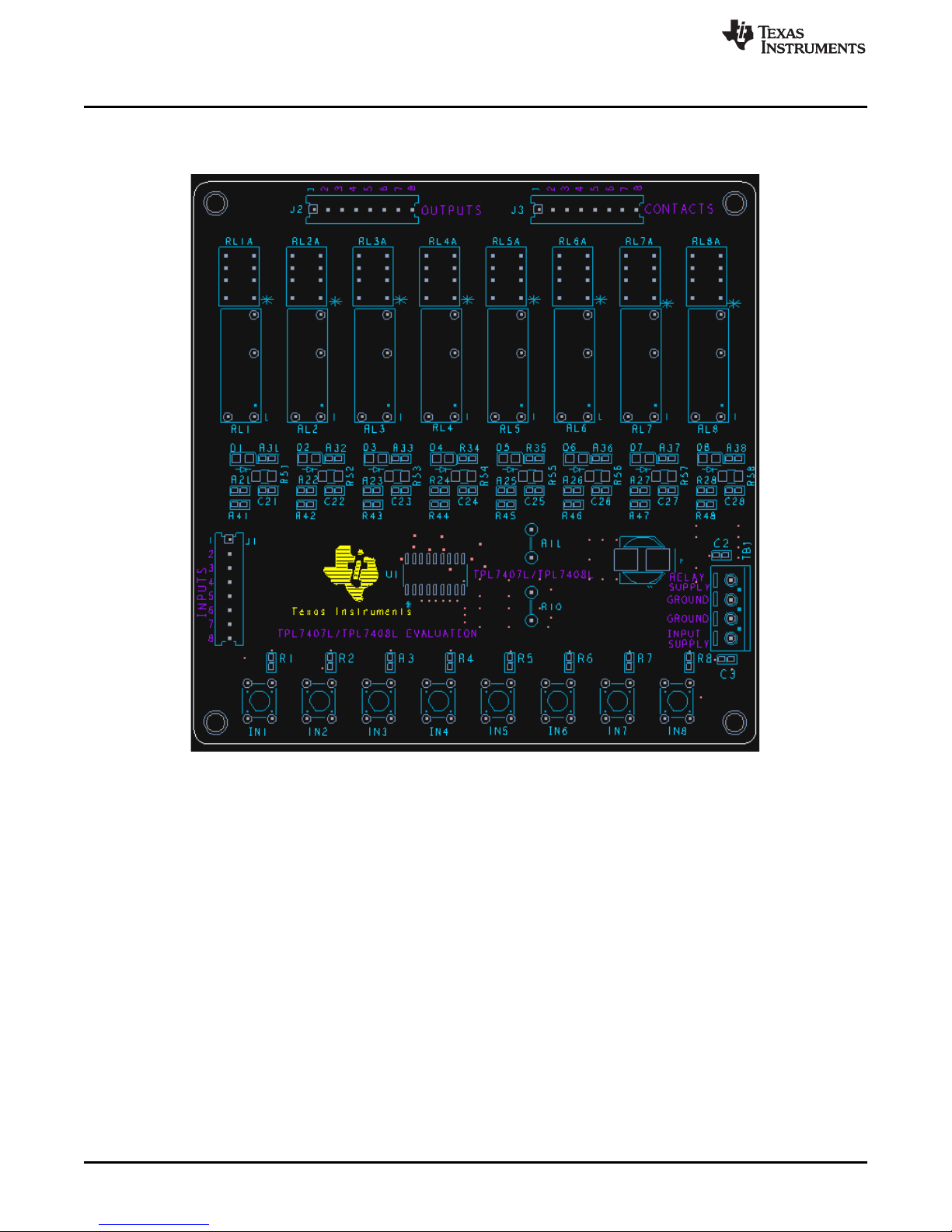
PCB Key Map
Physical structure for the TPL7407LEVM is illustrated in Figure 1.
www.ti.com
Figure 1. Physical Structure for the TPL7407LEVM (Approximate Layout)
2 Quick Setup Guide
This section describes the setup to quickly check the functionality of TPL7407LEVM.
2.1 Electrostatic Discharge Warning
Many of the components on the TPL7407LEVM are susceptible to damage by electrostatic discharge
(ESD). Customers are advised to observe proper ESD handling precautions when unpacking and handling
the EVM, including the use of a grounded wrist strap at an approved ESD workstation.
CAUTION: Failure to observe ESD handling procedures may result in damage to EVM components.
Unpacking the EVM
After opening the TPL7407LEVM package, check to ensure that the following items are included:
• 1 pc. TPL7407LEVM board using one TPL7407LDR
• 3 pc. Eight pin insulation displacement connectors that accept AWG 22 insulated wire.
2
TPL7407L7-Channel Relay and Inductive Load Sink Driver EVM SLRU005–February 2013
Copyright © 2013, Texas Instruments Incorporated
Submit Documentation Feedback
Page 3
TB1
Relay Supply ± 4
pin 8
Ground ± 3
Ground ± 2
Input Supply ± 1
C2 0.1F
C3
0.1F
+
470F
C1
C21-27
DNI
R21-R27 DNI
0
R51-R57
10K
R31-R37
D1
J2 - Output
IN1-7
COM
R41-R47
J3 - Contact
pins 1 - 7
TPL7407L
1 of 7
Channels
OUT1 - 7
J2 - Output
pins 1 - 7
J1 - Input
pin 1 - 7
J1 - Input
pin 8
R1-7
DNI
IN1-7
1M
Shared
GND
Regulation
Circuitry
DRIVER
50.
www.ti.com
Power Supply Setup
A 8.5V - 24V power supply capable of 500 mA of current is required.
Connect the positive power supply lead to the “Input Supply” on TB1-1 and also connect it to the “Relay
Supply” on TB1-4. Connect the negative power supply lead to either of the two ground connections on
TB1-2 or TB1-3.
It is important to connect the power supply correctly because opposite supply polarity will damage
the EVM.
Turn the power supply on. At this time, the EVM light emitting diodes (LEDS) should be off and no current
should be flowing from the power supply. The TPL7407L consumes no power when all seven channels
are off.
Press the pushbuttons labeled IN1 through IN7 one at a time. When pressed the corresponding relay will
click as the contacts engage and the LED will illuminate.
Releasing a pushbutton will disengage the corresponding relay contacts and extinguish the LED.
If all seven buttons operate as previously described, then the TPL7407LEVM passes functional testing.
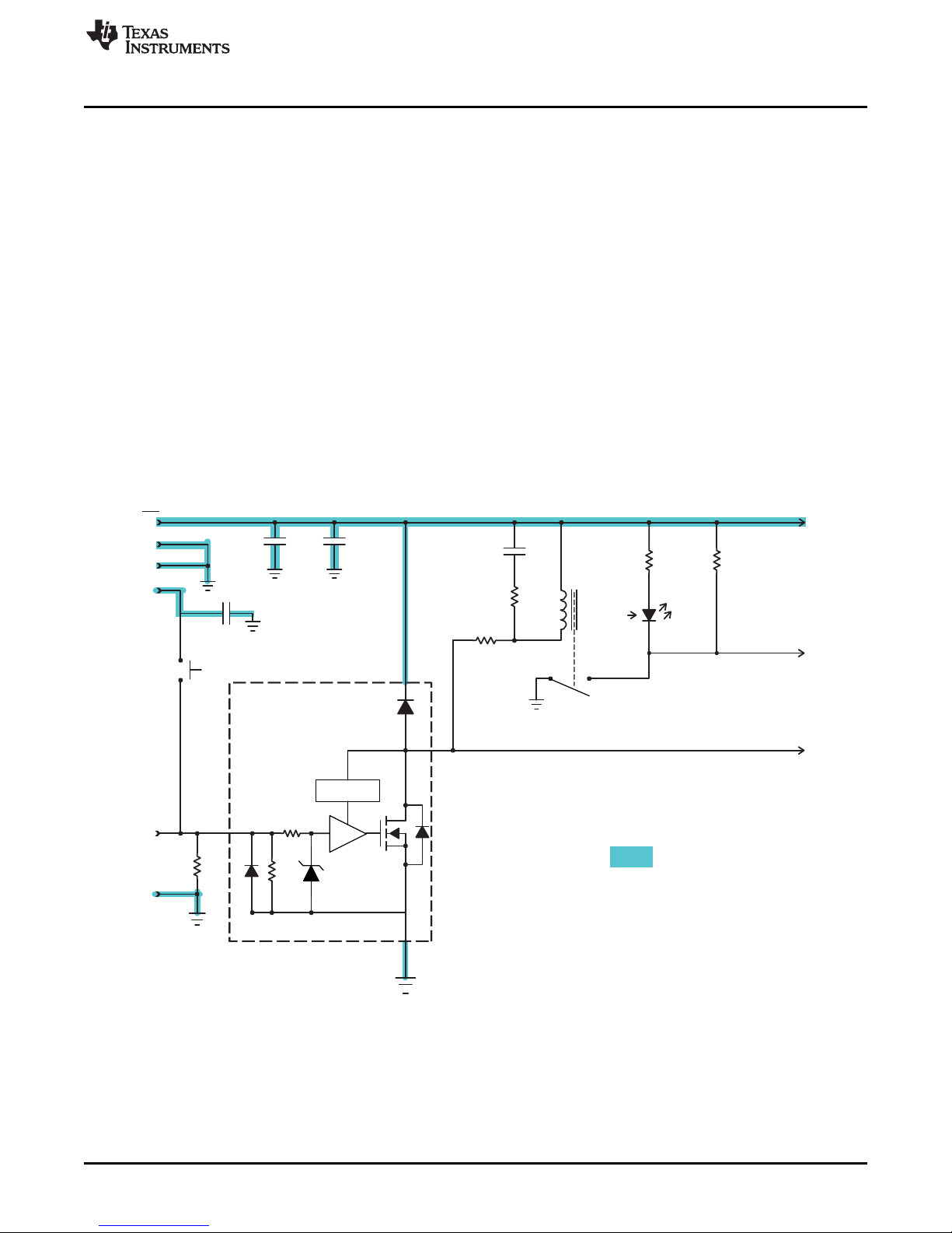
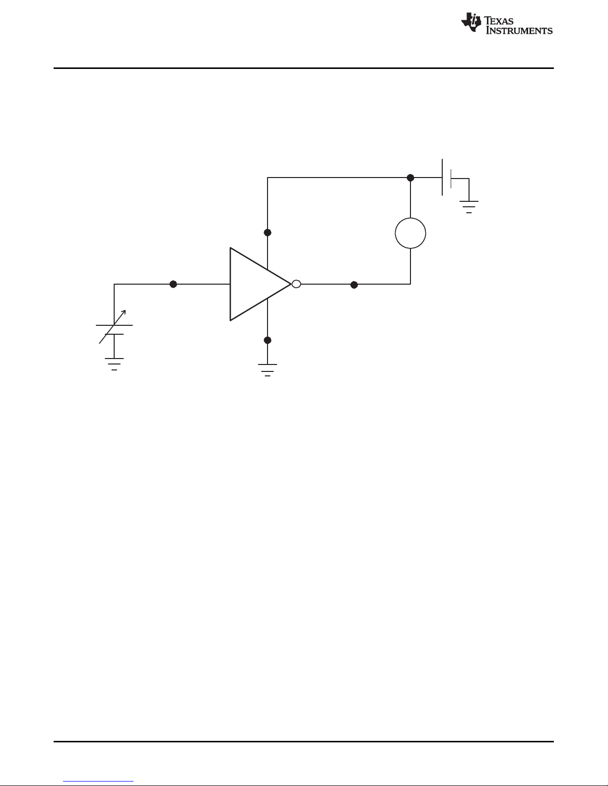
3 EVM Theory and Operation
The following single channel schematic is representative of the seven identical driver channels.
EVM Theory and Operation
The TPL7407LEVM is designed to accept an “Input Supply” on TB1-1 with a voltage range of 1.8V to 5.5V
and a “Relay Supply” on TB1-4 with a voltage range ideally set to 24V ±10%, but will still operate with a
minimum voltage of 8.5V and a maximum voltage of 40V.
SLRU005–February 2013 TPL7407L7-Channel Relay and Inductive Load Sink Driver EVM
Submit Documentation Feedback
Figure 2. Single Channel Schematic
Copyright © 2013, Texas Instruments Incorporated
3
Page 4

EVM Theory and Operation
When none of the buttons are pressed, the TPL7407L inputs will be open circuit and the internal resistors
in the TPL7407Lwill ensure zero volts on the inputs. With the inputs low, the TPL7407Loutput pins will set
to a high impedance state; therefore, no current will flow through the relay coils. The relay contact will not
be engaged and the voltage on the J3-Contact pins 1 to 7 will be pulled up to the relay supply voltage by a
10kΩ resistor on the PCB.
Pressing one of the input buttons, labeled IN1 to IN7, will apply the input voltage supply on TB1-1 to the
corresponding input pin on the TPL7407L. The internal resistor on the TPL7407L input pin will draw a
small current proportional to the input voltage. The nominal current is input voltage divided by 1MΩ, it can
also be expressed as the ratio, 1µA/V. The NMOS switch inside the TPL7407Lturns on providing a low
resistance path from output to ground. This completes the circuit and current flows from the relay supply
through the G5NB relay coil and through the TPL7407Loutput switch to ground and finally back through
the relay supply return lead. The relay coil current will engage the relay contacts. The relay contacts will
short the corresponding J3 “contact” pin to ground. It will also complete the corresponding LED circuit and
the LED will illuminate.
Releasing one of the input buttons, labeled IN1 to IN7, will remove the input voltage from the
corresponding input pin on the TPL7407L. The internal resistor on the TPL7407L input pin will decrease
the input voltage to zero. The NMOS switch inside the TPL7407Lturns off breaking the current path for the
relay coil. Since the coil is an inductor, the current cannot change in zero time. The coil voltage will
change polarity resulting in a TPL7407Loutput voltage that is greater than the relay supply voltage. This
will forward bias the diode inside the TPL7407Lpassing current back to the relay supply voltage. This
current will continue until the stored coil energy is depleted. The relay contacts will disengage and the
short on the J3-Contact pin will be removed and the pin voltage will increase back to the relay supply
voltage. The LED circuit will be open, thus extinguishing the LED.
The voltage on the output pins is always available on the J2-Output connector pins 1-7. Pin 8 is connected
to the COM pin on the TPL7407Land the relay supply voltage on TB1 pin 4. The J2-Output connector can
be used measure the output voltage. It can also be used to add additional loads to the TPL7407Loutput
pins. The series resistance between the J2-output connector and the TPL7407L is approximately 20 mΩ.
The onboard AGQ2003 relay coils can be removed from the TPL7407L by removing the seven 0Ω
resistors at locations R41 to R47.
The voltage on the input pins is always available on the J1-Input connector pins 1-7. Pin 8 is connected to
the GND pin on the TPL7407Land the ground voltage on TB1 pins 2 & 3. The J1-Input connector can be
used measure the input voltage. It can also be used to inject external signals onto the TPL7407Linput
pins.
Three user supplied components, per channel, can be added if needed. All three circuit board footprints
are SMD 0603 sized. The first location, R1 to R7, allows adding a resistor from each input to ground. The
second, R21 to R27, and third location, C21 to C27, are in series with each other and parallel with the
G5NB relay coils.
The terminal block, TB1, provides power for the input pushbuttons and relay coils. When directly
controlling the inputs using the J1-Input connector, the input source on TB1 pin1 may be disconnected.
The TPL7407L EVM board has seven identical channels. The single channel schematic is easier to read
then the complete schematic. The TPL7407Lsingle model functional diagram is enclosed by dotted lines.
The input pin has a 1MΩ resistor that keeps the driver off when no input is disconnected or put in to a high
impedance state. The NMOS transistor sinks to a shared ground connection when the input voltage is
applied. When the load is inductive and the NMOS turns off, the output voltage will increase beyond the
relay supply voltage and inductor current will continue to flow though the free wheeling diode to the COM
pin until the inductor is discharged.
Resistors R41 through R47 can be removed to isolate the output from the relay coils when external load
or automated test equipment is provided through the J2-Output connector.
The relay is an G5NB relay with a 2,880Ω, 24V, 8.3mA nominal coil. The pull-in voltage is less than 2.25V
(3V × 75%) and the drop out voltage is greater than 0.3V. The maximum coil voltage is 43.2V (24V ×
180%).
The relay contact when open will allow the J3-Contact pin to rise to the Relay supply voltage. The voltage
on J3-Contact connector can be measured by any high impedance (>100kΩ) measuring device. When the
contacts close the J2-Contact pin will be pulled down to ground potential.
www.ti.com
4
TPL7407L7-Channel Relay and Inductive Load Sink Driver EVM SLRU005–February 2013
Copyright © 2013, Texas Instruments Incorporated
Submit Documentation Feedback
Page 5
www.ti.com
TPL7407LEVM Performance Testing Using Lab Equipment
The TPL7407Loutput pins 16 to 10 are connected to relays RL1 to RL7 and J2-Output port pins 1 -7 (pin 8
is relay coil power sense).
The TPL7407LCOM, pin 9, is connected to the relay supply on TB1. This pin connects to the cathodes of
free wheeling diodes for each output. It provides a discharge path when the inductive load is turned off.
The inputs can be fully controlled by external test equipment using the J1-Input Port. The outputs can be
measured by external test equipment using the J2-Output Port. If relay supply voltage, TPL7407L COM
pin, exceeds 40V or full external control is required, then the relay coils should be disconnected by
removing the zero ohm resistors labeled R41 to R47.
The TPL7407LEVM has open 0603 foot prints for input resistors to ground as R11 to R17, coil wave
shaping resistor and capacitors as R31 to R37 and C31 to C37. The TPL7407L does not require these
components.
Increasing output load using onboard relays: Shorting two or more of the J2 pins 1-7 (output port) will
parallel the TPL7407Loutputs and relay coils. By activate just one of the inputs for the shorted output
channels will cause a single output to drive multiple relay coil loads. Two coils typically uses 16.6mA and
three coils typically use 24.9mA.
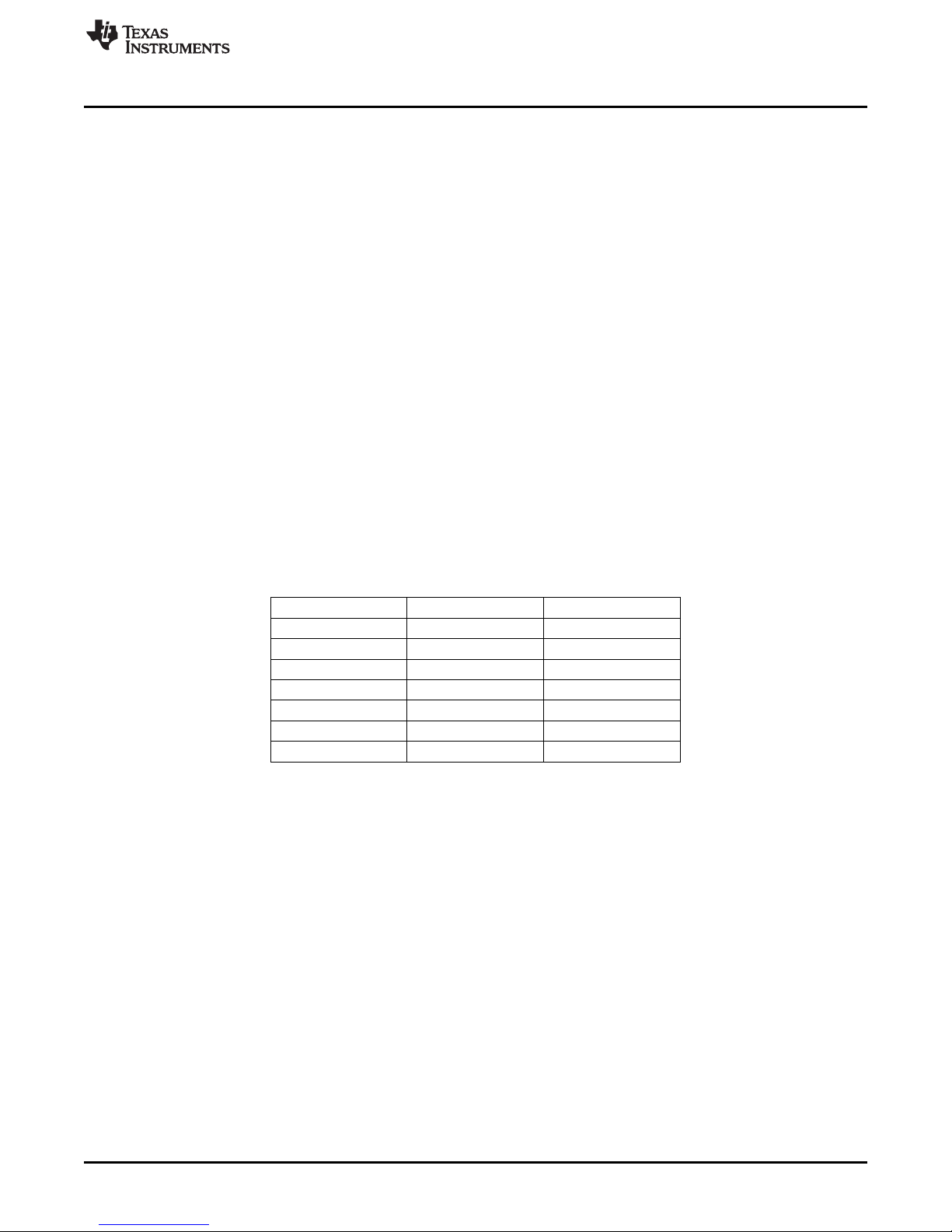
4 TPL7407LEVM Performance Testing Using Lab Equipment
Datasheet electrical characterization parameters can be measured using the following test setups. Setups
for both standard EVM boards and modified EVM boards that have R41 to R47 removed to disconnect the
onboard relay loads. It is acceptable to keep some channels “standard” (R4x installed) and other channels
“modified” (R4x removed). The capacitors (470µF & 0.1µF) on the TPL7407L COM pin are connected
regardless of R41 to R47 presence. Therefore the charging, discharging, and leakages of the capacitors
must be considered. Each output pin has an internal diode to the COM pin. Testing for channel 1 will be
described; test other channels by using a different pin on the J1(input) and J2(output) connectors.
Channel Tested J1(Input)-pin J2(Output)-pin
CH 1 J1–1 J2–1
CH 2 J1–2 J2–2
CH 3 J1–3 J2–3
CH 4 J1–4 J2–4
CH 5 J1–5 J2–5
CH 6 J1–6 J2–6
CH 7 J1–7 J2–7
Relay supply is connected to TB1 pin 4; the Relay supply sense line can also be connected to TB1-pin4.
Alternatively the sense line can be connected to J2 pin 8. The relay supply is the same node as the
TPL7407LCOM (pin 9).
Ground power and ground sense connection can be made to TB1 pins 2 and 3. An alternative ground
sense can be made at J1 pin 8.
Warning: All tests that supply current should be limited to the data sheet limit of 600mA. Input pin
voltage should be limited to 30V and output pin voltage should be limited to 40V.
SLRU005–February 2013 TPL7407L7-Channel Relay and Inductive Load Sink Driver EVM
Submit Documentation Feedback
5
Copyright © 2013, Texas Instruments Incorporated
Page 6
I
24V
Current
Limit 10 mA
TB1-4
Measure
Current
J1-1
IN
1/7
COM
OUT
J2-1
TPL7407L
Sweep
Voltage
0 to 1.5V
GND
TB1-2
TPL7407LEVM Performance Testing Using Lab Equipment
Input parameter VI(on) and VI(off) Channel 1 Test Setup and Typical Results
Board setup: Sweep input voltage on J1-1; Set Output J2-1 and Relay Supply to 24V, measure output
current on J2-1 [current clamp on measurement range of 10mA is recommended].
Note: any difference between voltage on J2-1 and Relay Supply(TB1-4) will affect low current accuracy
with Standard board.
www.ti.com
6
TPL7407L7-Channel Relay and Inductive Load Sink Driver EVM SLRU005–February 2013
Figure 3. VI(on) and VI(off) Schematic
Copyright © 2013, Texas Instruments Incorporated
Submit Documentation Feedback
Page 7

24 V
TB1-4
Measure
Current
J1-1
IN
1/7
COM
OUT
J2-1
I
Sweep
Voltage
0 to 5.5V
TPL7407L
GND
TB1-2
www.ti.com
TPL7407LEVM Performance Testing Using Lab Equipment
Input Parameter II(on) Channel 1 Test Setup and Typical Results
Input current is a function of input voltage alone. The output load impedance and termination voltage have
no impact on the results.
Board setup: Sweep input voltage on J1-1. Measure input current on J1-1. Optionally, Relay supply can be
connected to 24V.
SLRU005–February 2013 TPL7407L7-Channel Relay and Inductive Load Sink Driver EVM
Submit Documentation Feedback
Figure 4. II(on) Schematic
Copyright © 2013, Texas Instruments Incorporated
7
Page 8

24 V
TB1-4
Measure
Current
J1-1
IN
1/7
COM
OUT
J2-1
I
TPL7407L
GND
TB1-2
TB1-3
TPL7407LEVM Performance Testing Using Lab Equipment
Input Parameter II(off) Channel 1 Test Setup and Typical Results
Input current with zero input voltage will be very low. A pico-amp meter is recommended. This is a signal
point test.
Standard board setup: Set input voltage on J1-1 to 0V. Measure input current on J1-1. Optionally, output
J2-1 and Relay Supply can be set to 24V.
Modified board setup: Sweep CH1 voltage on J1-1; Set Output J2-1 and Relay Supply to 24V, measure
current on J1-1. The return lead of the pico-amp meter must be at board ground potential.
www.ti.com
8
TPL7407L7-Channel Relay and Inductive Load Sink Driver EVM SLRU005–February 2013
Figure 5. II(off) Schematic
Copyright © 2013, Texas Instruments Incorporated
Submit Documentation Feedback
Page 9

V
OPEN
TB1-4
J1-1
IN
1/7
COM
OUT
J2-1
Sweep
Current
TPL7407L
GND
Kelvin
0 to 500 mA
1.8V ± 5.0V
TB1-2
Connection
Measure
Voltage
TB-3
www.ti.com
TPL7407LEVM Performance Testing Using Lab Equipment
Output Parameter VOL Channel 1 Test Setup and Typical Results
This parameter was called collector emitter saturation voltage on the original TPL7407L device.
The data sheet has specifications for input voltages of 1.8V - 5V.
Board setup: Sweep output current on J2-1. Set desired input voltage on J1-1 [1.8V - 5V, and other
voltages]. Disconnect the relay supply on TB1-4. Measure output voltage on J2-1 (kelvin connections at
J2-1 and ground are highly recommended for accurate results).
SLRU005–February 2013 TPL7407L7-Channel Relay and Inductive Load Sink Driver EVM
Submit Documentation Feedback
Figure 6. VOL Schematic
Copyright © 2013, Texas Instruments Incorporated
9
Page 10

0.00
0.20
0.40
0.60
0.80
1.00
1.20
1.40
1.60
0 100 200 300 400 500 600 700
VOL (V)
Output Drain Current IDS(mA)
VOL at Various Temperatures
25C
70C
105C
-40C
TPL7407LEVM Performance Testing Using Lab Equipment
www.ti.com
Figure 7. VOL vs IOL
10
TPL7407L7-Channel Relay and Inductive Load Sink Driver EVM SLRU005–February 2013
Copyright © 2013, Texas Instruments Incorporated
Submit Documentation Feedback
Page 11

OPEN
TB1-4
J1-1
IN
1/7
COM
OUT
J2-1
Measure
Current
Sweep
Voltage
0 V to 5.5 V
TPL7407L
GND
TB1-2
I
SENSE
0.4 V
SENSE
TB1-3
www.ti.com
TPL7407LEVM Performance Testing Using Lab Equipment
Output Parameter IOUT(on) Channel 1 Test Setup and Typical Results
Board setup: Sweep input voltage on J1-1. Set output voltage on J2-1 to 0.4V. Disconnect the relay supply
on TB1-4. Measure output current on J2-1 (sense connections at J2-1 and ground are highly
recommended to keep 0.4V on the EVM regardless of line losses in wires and current meter).
SLRU005–February 2013 TPL7407L7-Channel Relay and Inductive Load Sink Driver EVM
Submit Documentation Feedback
Figure 8. IOUT(on) Schematic
Copyright © 2013, Texas Instruments Incorporated
11
Page 12

TEE
24V
Rising Edge
Slope
Trigger
50
J1-8
GND
J1-1
IN
1/7
TB1-4
COM
OUT
J2-8
COM
J2-1
50
10x Scope
3UREH³,QSXW´
GND
TB1-2
10x Scope
Probe
³2XWSXW´
3.3 V
Pulse Generator
100 kHz
0V
10% Duty Cycle
TPL7407L
TPL7407LEVM Performance Testing Using Lab Equipment
www.ti.com
Switching Parameter t
Board setup: The TPL7407Land TPL7407LEVM are primarily designed for slow responding loads like
relays, stepper motors, and DC lab equipment; however, the TPL7407Lrise/fall times and propagation
delays are short. Therefore line termination and short wires are important for signal quality. The waveform
below uses a 50 ohm cable “T” tapped within 3 cm of the J1-Input connector and terminated at the
oscilloscope set to 50 ohm input impedance. This input is used as the scope trigger. A locally grounded
10X scope probe is used to measure the input signal and the same probe was used to measure the output
on J2-1. A pull up resistor of 50Ω is connected between the output (J2-1) and Relay supply (J2-8). Set
scope trigger for rising edge. Pulse generator is 10% duty cycle 100kHz 3.3V logic level signal.
3.3V 50Ω Channel 1 Test Setup and Typical Results
PHL
Switching Parameter t
3.3V 50Ω Channel 1 Test Setup and Typical Results
PLH
Board setup: The TPL7407Land TPL7407LEVM are primarily designed for slow responding loads like
relays, stepper motors, and DC lab equipment; however, the TPL7407Lrise/fall times and propagation
delays are quite short. Therefore line termination and short wires are important for signal quality. The
waveform below uses a 50 ohm cable “T” tapped within 3 cm of the J1-Input connector and terminated at
the oscilloscope set to 50 ohm input impedance. This input is used as the scope trigger. A locally
grounded 10X scope probe is used to measure the input signal and the same probe was used to measure
the output on J2-1. A pull up resistor of 50Ω is connected between the output (J2-1) and Relay supply (J2-
8). Set scope trigger for falling edge. Pulse generator is 10% duty cycle 100kHz 3.3V logic level signal.
12
TPL7407L7-Channel Relay and Inductive Load Sink Driver EVM SLRU005–February 2013
Figure 9. T
Copyright © 2013, Texas Instruments Incorporated
Schematic
PHL
Submit Documentation Feedback
Page 13

TEE
24V
Falling Edge
Slope
Trigger
50
J1-8
GND
J1-1
IN
1/7
TB1-4
COM
OUT
J2-8
COM
J2-1
50
10x Scope
3UREH³,QSXW´
GND
TB1-2
10x Scope
Probe
³2XWSXW´
3.3 V
Pulse Generator
100 kHz
0V
10% Duty Cycle
TPL7407L
www.ti.com
TPL7407LEVM Performance Testing Using Lab Equipment
Switching Parameter RINChannel 1 Test Setup and Typical Results.
The data to calculate RIN, the DC input resistance, was recorded during the II(on) test. The input
resistance is simply input voltage divided by input current.
SLRU005–February 2013 TPL7407L7-Channel Relay and Inductive Load Sink Driver EVM
Submit Documentation Feedback
Figure 10. T
Copyright © 2013, Texas Instruments Incorporated
Schematic
PLH
13
Page 14

J1-1
IN
1/7
TB1-4
COM
OUT
Measure
Voltage
V
J2-1
OPEN
Sweep
GND
TB1-2
Current
0 to 600 mA
TPL7407L
TPL7407LEVM Performance Testing Using Lab Equipment
Free-wheeling Diode Parameter VF channel 1 Test Setup and Typical Results
Board setup: Sweep output current on J2-1. Set Relay supply voltage to 0V. On standard boards the X
axis (output current) will need to be compensated for coil current flow. The real diode current is
approximately X-VF/2,880Ω. Measure output current on J2-1 (Kelvin connections at J2-1 and relay supply
are highly recommended for accurate results).
www.ti.com
14
TPL7407L7-Channel Relay and Inductive Load Sink Driver EVM SLRU005–February 2013
Figure 11. VF Schematic
Copyright © 2013, Texas Instruments Incorporated
Submit Documentation Feedback
Page 15

0.000
0.100
0.200
0.300
0.400
0.500
0.600
0.700
0.800
0.000 0.200 0.400 0.600 0.800 1.000 1.200 1.400 1.600
IF (A)
VF (V)
Fly-back Diode Forward Voltage
www.ti.com
TPL7407LEVM Performance Testing Using Lab Equipment
Figure 12. VF = Diode(V) vs Diode(I)
SLRU005–February 2013 TPL7407L7-Channel Relay and Inductive Load Sink Driver EVM
Submit Documentation Feedback
15
Copyright © 2013, Texas Instruments Incorporated
Page 16

OUT4
OUT7
OUT1
OUT2
OUT3
OUT5
OUT6
OUT8
IN1
IN2
IN3
IN4
IN5
IN6
IN7
IN8
OUT8
OUT7
OUT6
OUT5
OUT4
OUT3
OUT2
OUT1
V_RELAY
V_RELAY
V_IN
V_IN
V_IN
OUT1
OUT2
OUT3
OUT4
OUT5
OUT6
OUT7
OUT8
CONTACT1
CONTACT2
CONTACT3
CONTACT4
CONTACT5
CONTACT6
CONTACT7
CONTACT8
R3R
DNI
R3R
DNI
IN8
SPST
DNI
IN8
SPST
DNI
142
3
R5R
DNI
R5R
DNI
R7R
DNI
R7R
DNI
+
C1
470UF
+
C1
470UF
J3
8 HEADERJ38 HEADER
1234567
8
U1
ULN2003LVDR
U1
P11P22P33P44P55P66P77P88P9
9
P1010P1111P1212P1313P1414P1515P1616P1717P18
18
R1R
DNI
R1R
DNI
MTG4MTG4
MTG3MTG3
IN5
SPST
IN5
SPST
142
3
MTG2MTG2
TB1
TERM BLOCK
TB1
TERM BLOCK
123
4
C2
0.1UFC20.1UF
MTG1MTG1
C3
0.1UFC30.1UF
R4R
DNI
R4R
DNI
J2
8 HEADERJ28 HEADER
1234567
8
R100R10
0
R6R
DNI
R6R
DNI
R11 0R11 0
IN1
SPST
IN1
SPST
142
3
R8R
DNI
R8R
DNI
R2R
DNI
R2R
DNI
IN7
SPST
IN7
SPST
142
3
IN2
SPST
IN2
SPST
142
3
IN3
SPST
IN3
SPST
142
3
IN4
SPST
IN4
SPST
142
3
IN6
SPST
IN6
SPST
142
3
J1
8 HEADERJ18 HEADER
1234567
8
TPL7407LEVM Performance Testing Using Lab Equipment
www.ti.com
16
TPL7407L7-Channel Relay and Inductive Load Sink Driver EVM SLRU005–February 2013
Figure 13. Full Schematic
Copyright © 2013, Texas Instruments Incorporated
Submit Documentation Feedback
Page 17

Evaluation Board/Kit Important Notice
Texas Instruments (TI) provides the enclosed product(s) under the following conditions:
This evaluation board/kit is intended for use for ENGINEERING DEVELOPMENT, DEMONSTRATION, OR EVALUATION PURPOSES
ONLY and is not considered by TI to be a finished end-product fit for general consumer use. Persons handling the product(s) must have
electronics training and observe good engineering practice standards. As such, the goods being provided are not intended to be complete
in terms of required design-, marketing-, and/or manufacturing-related protective considerations, including product safety and environmental
measures typically found in end products that incorporate such semiconductor components or circuit boards. This evaluation board/kit does
not fall within the scope of the European Union directives regarding electromagnetic compatibility, restricted substances (RoHS), recycling
(WEEE), FCC, CE or UL, and therefore may not meet the technical requirements of these directives or other related directives.
Should this evaluation board/kit not meet the specifications indicated in the User’s Guide, the board/kit may be returned within 30 days from
the date of delivery for a full refund. THE FOREGOING WARRANTY IS THE EXCLUSIVE WARRANTY MADE BY SELLER TO BUYER
AND IS IN LIEU OF ALL OTHER WARRANTIES, EXPRESSED, IMPLIED, OR STATUTORY, INCLUDING ANY WARRANTY OF
MERCHANTABILITY OR FITNESS FOR ANY PARTICULAR PURPOSE.
The user assumes all responsibility and liability for proper and safe handling of the goods. Further, the user indemnifies TI from all claims
arising from the handling or use of the goods. Due to the open construction of the product, it is the user’s responsibility to take any and all
appropriate precautions with regard to electrostatic discharge.
EXCEPT TO THE EXTENT OF THE INDEMNITY SET FORTH ABOVE, NEITHER PARTY SHALL BE LIABLE TO THE OTHER FOR ANY
INDIRECT, SPECIAL, INCIDENTAL, OR CONSEQUENTIAL DAMAGES.
TI currently deals with a variety of customers for products, and therefore our arrangement with the user is not exclusive.
TI assumes no liability for applications assistance, customer product design, software performance, or infringement of patents or
services described herein.
Please read the User’s Guide and, specifically, the Warnings and Restrictions notice in the User’s Guide prior to handling the product. This
notice contains important safety information about temperatures and voltages. For additional information on TI’s environmental and/or
safety programs, please contact the TI application engineer or visit www.ti.com/esh.
No license is granted under any patent right or other intellectual property right of TI covering or relating to any machine, process, or
combination in which such TI products or services might be or are used.
FCC Warning
This evaluation board/kit is intended for use for ENGINEERING DEVELOPMENT, DEMONSTRATION, OR EVALUATION PURPOSES
ONLY and is not considered by TI to be a finished end-product fit for general consumer use. It generates, uses, and can radiate radio
frequency energy and has not been tested for compliance with the limits of computing devices pursuant to part 15 of FCC rules, which are
designed to provide reasonable protection against radio frequency interference. Operation of this equipment in other environments may
cause interference with radio communications, in which case the user at his own expense will be required to take whatever measures may
be required to correct this interference.
EVM Warnings and Restrictions
It is important to operate this EVM within the input voltage range of and the output voltage range of .
Exceeding the specified input range may cause unexpected operation and/or irreversible damage to the EVM. If there are questions
concerning the input range, please contact a TI field representative prior to connecting the input power.
Applying loads outside of the specified output range may result in unintended operation and/or possible permanent damage to the EVM.
Please consult the EVM User's Guide prior to connecting any load to the EVM output. If there is uncertainty as to the load specification,
please contact a TI field representative.
During normal operation, some circuit components may have case temperatures greater than . The EVM is designed to operate properly
with certain components above as long as the input and output ranges are maintained. These components include but are not limited to
linear regulators, switching transistors, pass transistors, and current sense resistors. These types of devices can be identified using the
EVM schematic located in the EVM User's Guide. When placing measurement probes near these devices during operation, please be
aware that these devices may be very warm to the touch.
Mailing Address: Texas Instruments, Post Office Box 655303, Dallas, Texas 75265
Copyright © 2014, Texas Instruments Incorporated
Page 18

IMPORTANT NOTICE
Texas Instruments Incorporated and its subsidiaries (TI) reserve the right to make corrections, enhancements, improvements and other
changes to its semiconductor products and services per JESD46, latest issue, and to discontinue any product or service per JESD48, latest
issue. Buyers should obtain the latest relevant information before placing orders and should verify that such information is current and
complete. All semiconductor products (also referred to herein as “components”) are sold subject to TI’s terms and conditions of sale
supplied at the time of order acknowledgment.
TI warrants performance of its components to the specifications applicable at the time of sale, in accordance with the warranty in TI’s terms
and conditions of sale of semiconductor products. Testing and other quality control techniques are used to the extent TI deems necessary
to support this warranty. Except where mandated by applicable law, testing of all parameters of each component is not necessarily
performed.
TI assumes no liability for applications assistance or the design of Buyers’ products. Buyers are responsible for their products and
applications using TI components. To minimize the risks associated with Buyers’ products and applications, Buyers should provide
adequate design and operating safeguards.
TI does not warrant or represent that any license, either express or implied, is granted under any patent right, copyright, mask work right, or
other intellectual property right relating to any combination, machine, or process in which TI components or services are used. Information
published by TI regarding third-party products or services does not constitute a license to use such products or services or a warranty or
endorsement thereof. Use of such information may require a license from a third party under the patents or other intellectual property of the
third party, or a license from TI under the patents or other intellectual property of TI.
Reproduction of significant portions of TI information in TI data books or data sheets is permissible only if reproduction is without alteration
and is accompanied by all associated warranties, conditions, limitations, and notices. TI is not responsible or liable for such altered
documentation. Information of third parties may be subject to additional restrictions.
Resale of TI components or services with statements different from or beyond the parameters stated by TI for that component or service
voids all express and any implied warranties for the associated TI component or service and is an unfair and deceptive business practice.
TI is not responsible or liable for any such statements.
Buyer acknowledges and agrees that it is solely responsible for compliance with all legal, regulatory and safety-related requirements
concerning its products, and any use of TI components in its applications, notwithstanding any applications-related information or support
that may be provided by TI. Buyer represents and agrees that it has all the necessary expertise to create and implement safeguards which
anticipate dangerous consequences of failures, monitor failures and their consequences, lessen the likelihood of failures that might cause
harm and take appropriate remedial actions. Buyer will fully indemnify TI and its representatives against any damages arising out of the use
of any TI components in safety-critical applications.
In some cases, TI components may be promoted specifically to facilitate safety-related applications. With such components, TI’s goal is to
help enable customers to design and create their own end-product solutions that meet applicable functional safety standards and
requirements. Nonetheless, such components are subject to these terms.
No TI components are authorized for use in FDA Class III (or similar life-critical medical equipment) unless authorized officers of the parties
have executed a special agreement specifically governing such use.
Only those TI components which TI has specifically designated as military grade or “enhanced plastic” are designed and intended for use in
military/aerospace applications or environments. Buyer acknowledges and agrees that any military or aerospace use of TI components
which have not been so designated is solely at the Buyer's risk, and that Buyer is solely responsible for compliance with all legal and
regulatory requirements in connection with such use.
TI has specifically designated certain components as meeting ISO/TS16949 requirements, mainly for automotive use. In any case of use of
non-designated products, TI will not be responsible for any failure to meet ISO/TS16949.
Products Applications
Audio www.ti.com/audio Automotive and Transportation www.ti.com/automotive
Amplifiers amplifier.ti.com Communications and Telecom www.ti.com/communications
Data Converters dataconverter.ti.com Computers and Peripherals www.ti.com/computers
DLP® Products www.dlp.com Consumer Electronics www.ti.com/consumer-apps
DSP dsp.ti.com Energy and Lighting www.ti.com/energy
Clocks and Timers www.ti.com/clocks Industrial www.ti.com/industrial
Interface interface.ti.com Medical www.ti.com/medical
Logic logic.ti.com Security www.ti.com/security
Power Mgmt power.ti.com Space, Avionics and Defense www.ti.com/space-avionics-defense
Microcontrollers microcontroller.ti.com Video and Imaging www.ti.com/video
RFID www.ti-rfid.com
OMAP Applications Processors www.ti.com/omap TI E2E Community e2e.ti.com
Wireless Connectivity www.ti.com/wirelessconnectivity
Mailing Address: Texas Instruments, Post Office Box 655303, Dallas, Texas 75265
Copyright © 2014, Texas Instruments Incorporated
Page 19

Mouser Electronics
Authorized Distributor
Click to View Pricing, Inventory, Delivery & Lifecycle Information:
Texas Instruments:
TPL7407LEVM
 Loading...