

Page 1
GND
GPIO
V
IN+
V
IN-
ALERT
SDA
SCL
ADC
TMP512
TMP513
DXP1
DXN1
DXP2
DXN2
Subregulator
3.3V
V+
Filter C
Two-Wire
Interface
Power Register
Current Register
Voltage Register
ADC
Low-Pass Filter
Internal
Diode
Temperature
Sensor
Mux
A0
DXP3
DXN3
TMP512
TMP513
www.ti.com
SBOS491 –JUNE 2010
Temperature and Power Supply System Monitors
Check for Samples: TMP512, TMP513
1
FEATURES
234
• ±1°C REMOTE DIODE SENSORS
• ±1°C LOCAL TEMPERATURE SENSOR
• SERIES RESISTANCE CANCELLATION
• n-FACTOR CORRECTION
• TEMPERATURE ALERT FUNCTION temperatures, on-chip temperatures, and system
• AVERAGING
• 12-BIT RESOLUTION
• DIODE FAULT DETECTION
• SENSES BUS VOLTAGES FROM 0V TO +26V
• REPORTS CURRENT IN AMPS, VOLTAGE IN Remote accuracy is ±1°C for multiple IC
VOLTS AND POWER IN WATTS
• HIGH ACCURACY: 1% MAX OVER TEMP
• WATCHDOG LIMITS:
– Upper Over-Limit
– Lower Under-Limit
APPLICATIONS
• DESKTOP AND NOTEBOOK COMPUTERS
• SERVERS
• INDUSTRIAL CONTROLLERS
• CENTRAL OFFICE TELECOM EQUIPMENT
• LCD/ DLP®/LCOS PROJECTORS
• STORAGE AREA NETWORKS (SAN)
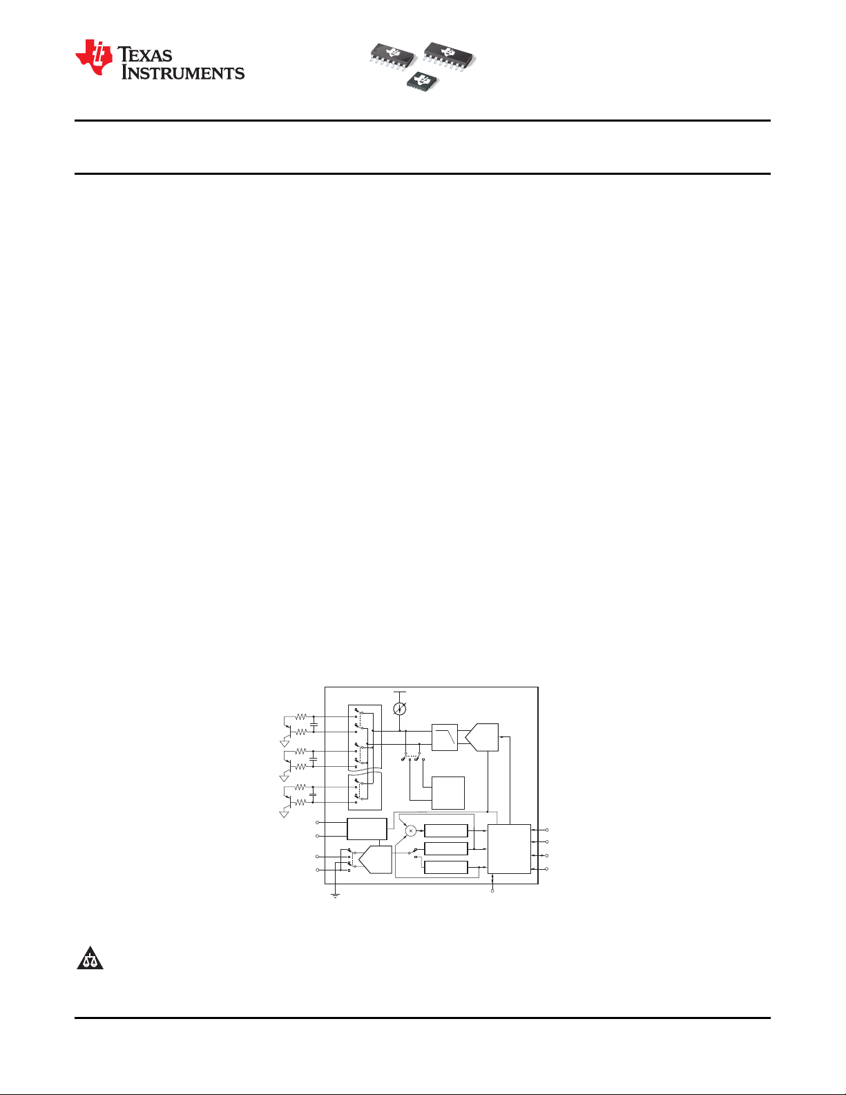
DESCRIPTION
The TMP512 (dual-channel) and TMP513
(triple-channel) are system monitors that include
remote sensors, a local temperature sensor, and a
high-side current shunt monitor. These system
monitors have the capability of measuring remote
voltage/power/current consumption.
The remote temperature sensor diode-connected
transistors are typically low-cost, NPN- or PNP-type
transistors or diodes that are an integral part of
microcontrollers, microprocessors, or FPGAs.
manufacturers, with no calibration needed. The
two-wire serial interface accepts SMBus™ or
two-wire write and read commands.
The onboard current shunt monitor is a high-side
current shunt and power monitor. It monitors both the
shunt drop and supply voltage. A programmable
calibration value (along with the TMP512/TMP513
internal digital multiplier) enables direct readout in
amps; an additional multiplication calculates power in
watts. The TMP512 and TMP513 both feature two
separate onboard watchdog capabilities: an over-limit
comparator and a lower-limit comparator.
These devices use a single +3V to +26V supply,
drawing a maximum of 1.4mA of supply current, and
they are specified for operation from –40°C to
+125°C.
1
2DLP is a registered trademark of Texas Instruments.
3SMBus is a trademark of Intel Corporation.
4All other trademarks are the property of their respective owners.
UNLESS OTHERWISE NOTED this document contains
PRODUCTION DATA information current as of publication date.
Products conform to specifications per the terms of Texas
Instruments standard warranty. Production processing does not
necessarily include testing of all parameters.
Please be aware that an important notice concerning availability, standard warranty, and use in critical applications of Texas
Instruments semiconductor products and disclaimers thereto appears at the end of this data sheet.
Copyright © 2010, Texas Instruments Incorporated
Page 2
TMP512
TMP513
SBOS491 –JUNE 2010
www.ti.com
This integrated circuit can be damaged by ESD. Texas Instruments recommends that all integrated circuits be handled with
appropriate precautions. Failure to observe proper handling and installation procedures can cause damage.
ESD damage can range from subtle performance degradation to complete device failure. Precision integrated circuits may be more
susceptible to damage because very small parametric changes could cause the device not to meet its published specifications.
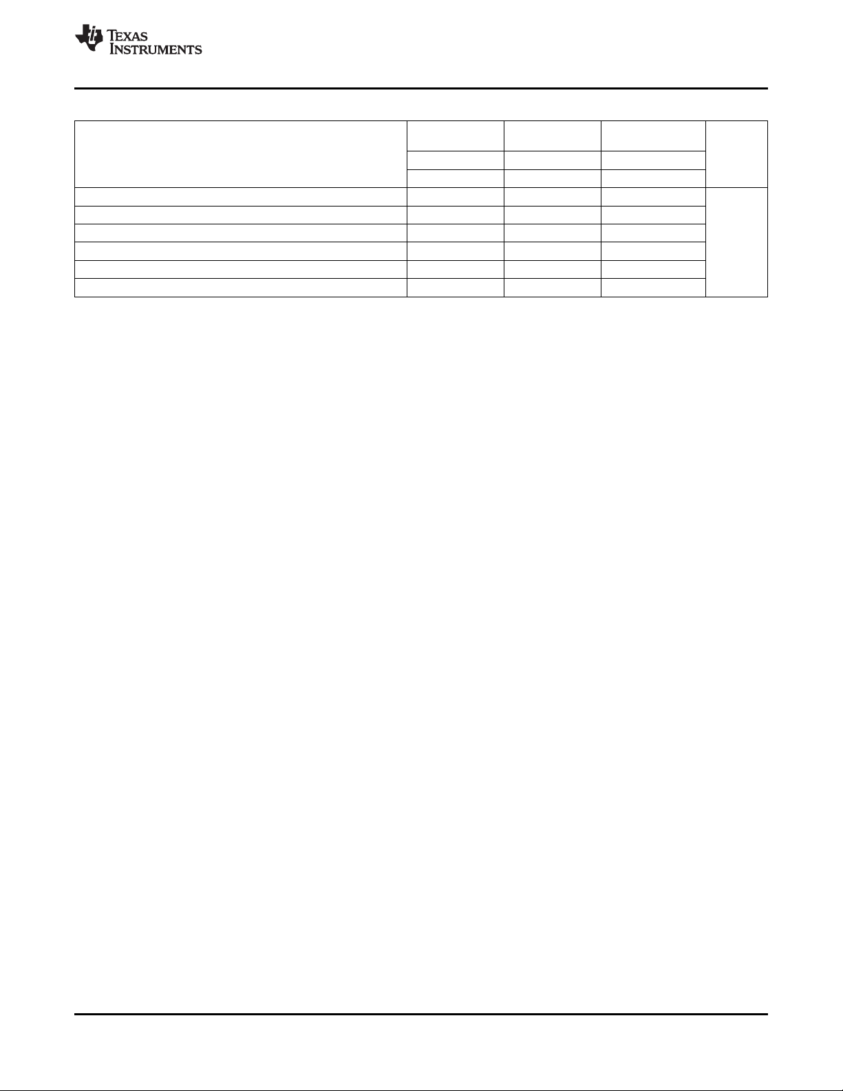
PACKAGE INFORMATION
(1)
PRODUCT PACKAGE-LEAD PACKAGE DESIGNATOR PACKAGE MARKING
TMP512 SO-14 D TMP512A
TMP513
SO-16 D TMP513A
(2)
QFN-16
RSA TMP513A
(1) For the most current package and ordering information see the Package Option Addendum at the end of this document, or visit the
TMP512/TMP513 product folder at www.ti.com.
(2) Product preview device.
ABSOLUTE MAXIMUM RATINGS
(1)
Over operating free-air temperature range (unless otherwise noted).
TMP512, TMP513 UNIT
Supply Voltage, V+ 26 V
Filter C
Analog Inputs, V
IN+
, V
IN–
Open-Drain Digital Outputs GND – 0.3 to +6 V
GPIO, DXP, DXN GND – 0.3 to V+ + 0.3 V
Input Current Into Any Pin 5 mA
Open-Drain Digital Output Current 10 mA
Storage Temperature –65 to +150 °C
Junction Temperature +150 °C
ESD Ratings Charged-Device Model (CDM) 1000 V
(1) Stresses above these ratings may cause permanent damage. Exposure to absolute maximum conditions for extended periods may
degrade device reliability. These are stress ratings only, and functional operation of the device at these or any other conditions beyond
those specified is not implied.
(2) V
IN+
+26V.
and V
may have a differential voltage of –26V to +26V; however, the voltage at these pins must not exceed the range –0.3V to
IN–
Voltage GND – 0.3 to +6 V
Current 10 mA
Differential (V
IN+
) – (V
IN–
(2)
)
–26 to +26 V
Common-Mode –0.3 to +26 V
Human Body Model (HBM) 2000 V
Machine Model (MM) 150 V
2 Submit Documentation Feedback Copyright © 2010, Texas Instruments Incorporated
Product Folder Link(s): TMP512 TMP513
Page 3
TMP512
TMP513
www.ti.com
SBOS491 –JUNE 2010
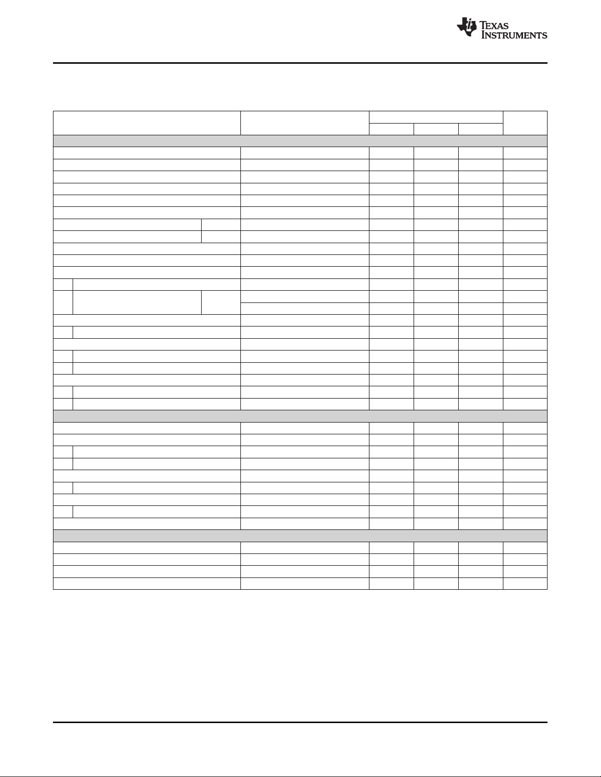
THERMAL INFORMATION
TMP512 TMP513AID
THERMAL METRIC
(1)
D (SOIC) D (SOIC) RSA
14 16 16
q
JA
q
JC(top)
q
JB
y
JT
y
JB
q
JC(bottom)
Junction-to-ambient thermal resistance
Junction-to-case(top) thermal resistance
Junction-to-board thermal resistance
Junction-to-top characterization parameter
Junction-to-board characterization parameter
Junction-to-case(bottom) thermal resistance
(2)
(3)
(4)
(5)
(6)
(7)
91.1 77.6 44.8
10.6 55.0 43.8
40.3 49.9 14.7
49.1 3.5 0.4
47.5 32.2 14.5
n/a n/a 2.6
(1) For more information about traditional and new thermal metrics, see the IC Package Thermal Metrics application report, SPRA953.
(2) The junction-to-ambient thermal resistance under natural convection is obtained in a simulation on a JEDEC-standard, high-K board, as
specified in JESD51-7, in an environment described in JESD51-2a.
(3) The junction-to-case (top) thermal resistance is obtained by simulating a cold plate test on the package top. No specific
JEDEC-standard test exists, but a close description can be found in the ANSI SEMI standard G30-88.
(4) The junction-to-board thermal resistance is obtained by simulating in an environment with a ring cold plate fixture to control the PCB
temperature, as described in JESD51-8.
(5) The junction-to-top characterization parameter, yJT, estimates the junction temperature of a device in a real system and is extracted
from the simulation data for obtaining qJA, using a procedure described in JESD51-2a (sections 6 and 7).
(6) The junction-to-board characterization parameter, yJB, estimates the junction temperature of a device in a real system and is extracted
from the simulation data for obtaining qJA, using a procedure described in JESD51-2a (sections 6 and 7).
(7) The junction-to-case (bottom) thermal resistance is obtained by simulating a cold plate test on the exposed (power) pad. No specific
JEDEC standard test exists, but a close description can be found in the ANSI SEMI standard G30-88.
TMP513AIRSAR
TMP513AIRSAT
UNITS
°C/W
Copyright © 2010, Texas Instruments Incorporated Submit Documentation Feedback 3
Product Folder Link(s): TMP512 TMP513
Page 4
TMP512
TMP513
SBOS491 –JUNE 2010
www.ti.com
ELECTRICAL CHARACTERISTICS: V+ = +12V
Boldface limits apply over the specified temperature range, TA= –40°C to +125°C.
At TA= +25°C, V+ = 12V, V
PARAMETER TEST CONDITIONS MIN TYP MAX UNIT
INPUT
Current Sense (Input) Voltage Range PGA = ÷ 1 0 ±40 mV
Bus Voltage (Input Voltage) Range
Common-Mode Rejection CMRR V
Offset Voltage, RTI
vs Temperature 0.2 mV/°C
vs Power Supply PSRR
Current Sense Gain Error ±0.04 %
vs Temperature 0.0025 %
Input Impedance Active Mode
V
IN+
V
IN–
Input Leakage Power-Down Mode
V
IN+
V
IN–
DC ACCURACY
ADC Basic Resolution 12 Bits
1 LSB Step Size
Shunt Voltage 10 mV
Bus Voltage 4 mV
Current Measurement Error ±0.2 ±0.5 %
over Temperature ±1 %
Bus Voltage Measurement Error ±0.2 ±0.5 %
over Temperature ±1 %
Differential Nonlinearity ±0.1 LSB
ADC TIMING
ADC Conversion Time 12-Bit 665 733 ms
(1) BRNG is bit 13 of Configuration Register 1.
(2) This parameter only expresses the full-scale range of the ADC scaling. In no event should more than 26V be applied to this device.
(3) Referred-to-input (RTI).
(4) See Subregulator section.
(3)
Pin 20 mA
Pin 20 || 320 mA || kΩ
Pin 0.1 0.5 mA
Pin 0.1 0.5 mA
SENSE
(2)
= (V
IN+
– V
) = 32mV, PGA = ÷ 1, and BRNG
IN–
PGA = ÷ 2 0 ±80 mV
PGA = ÷ 4 0 ±160 mV
PGA = ÷ 8 0 ±320 mV
BRNG = 0 0 16 V
BRNG = 1 0 32 V
= 0V to 26V 100 120 dB
IN+
V
OS
V+ = 3V to 5.5V, Configuration 3
V+ = 4.5V to 26V, subregulator supply 0.1 mV/V
PGA = ÷ 1 ±10 ±100 mV
PGA = ÷ 2 ±20 ±125 mV
PGA = ÷ 4 ±30 ±150 mV
PGA = ÷ 8 ±40 ±200 mV
11-Bit 345 380 ms
10-Bit 185 204 ms
9-Bit 105 117 ms
(1)
= 1, unless otherwise noted.
TMP512, TMP513
(4)
10 mV/V
4 Submit Documentation Feedback Copyright © 2010, Texas Instruments Incorporated
Product Folder Link(s): TMP512 TMP513
Page 5
TMP512
TMP513
www.ti.com
SBOS491 –JUNE 2010
ELECTRICAL CHARACTERISTICS: V+ = +12V (continued)
Boldface limits apply over the specified temperature range, TA= –40°C to +125°C.
At TA= +25°C, V+ = 12V, V
PARAMETER TEST CONDITIONS MIN TYP MAX UNIT
TEMPERATURE ERROR
Local Temperature Sensor TE
Remote Temperature Sensor
vs Supply, Local V+ = 3V to 5.5V, Configuration 3
vs Supply, Remote
TEMPERATURE MEASUREMENT
Conversion Time (per channel) 100 115 130 ms
Resolution
Local Temperature Sensor 13 Bits
Remote Temperature Sensor 13 Bits
Remote Sensor Source Currents Series Resistance 3kΩ max
High 120 mA
Medium High 60 mA
Medium Low 12 mA
Low 6 mA
Default Non-Ideality Factor n TMP512/12 Optimized Ideality Factor 1.008
SMBus
Logic Input High Voltage (SCL, SDA, GPIO,
A0)
Logic Input Low Voltage (SCL, SDA, GPIO,
A0)
Hysteresis 500 mV
SMBus Output Low Sink Current 6 mA
SDA Output Low Voltage V
Logic Input Current 0 ≤ VIN≤ 6V –1 1 mA
SMBus Input Capacitance (SCL, SDA, GPIO, A0) 3 pF
SMBus Clock Frequency 3.4 MHz
SMBus Timeout
SCL Falling Edge to SDA Valid Time 1 ms
POWER SUPPLY
Specified Supply Range
Quiescent Current 1 1.4 mA
Quiescent Current, Power-Down Mode 55 100 mA
Power-On Reset Threshold 2 V
TEMPERATURE RANGE
Specified Temperature Range –40 +125 °C
(7)
(5) Tested with one-shot measurements, and with less than 5Ω effective series resistance, and with 100pF differential input capacitance.
(6) See Subregulator section.
(7) SMBus timeout in the TMP512/13 resets the interface any time SCL or SDA is low for over 28ms.
(5)
(6)
SENSE
= (V
– V
IN+
) = 32mV, PGA = ÷ 1, and BRNG
IN–
LOCAL
TE
REMOTE
V
IH
V
IL
OL
V+ +3 +26 V
TA= –40°C to +125°C ±1.25 ±2.5 °C
TA= +15°C to +85°C, V+ = 12V ±0.25 ±1 °C
TA= +15°C to +85°C, TD= –40°C to+
TA= –40°C to +100°C, TD= –40°C to
TA= –40°C to +125°C, TD= –40°C to
V+ = 4.5V to 26V, subregulator supply 0.01 0.05 °C/V
150°C, V+ = 12V
+150°C, V+ = 12V
+150°C
V+ = 3V to 5.5V, Configuration 3
I
= 6mA 0.15 0.4 V
OUT
(1)
= 1, unless otherwise noted.
TMP512, TMP513
±0.25 ±1 °C
(6)
(6)
2.1 V
25 30 35 ms
±1 ±3 °C
±3 ±5 °C
0.2 0.5 °C/V
0.2 0.5 °C/V
0.8 V
Copyright © 2010, Texas Instruments Incorporated Submit Documentation Feedback 5
Product Folder Link(s): TMP512 TMP513
Page 6

1
2
3
4
5
6
7
V
IN-
SDA
SCL
A0
V
IN+
V+
Filter C
DXP2
DXN1
DXP1
GPIO
ALERT
GND
DXN2
14
13
12
11
10
9
8
TMP512
TMP512
TMP513
SBOS491 –JUNE 2010
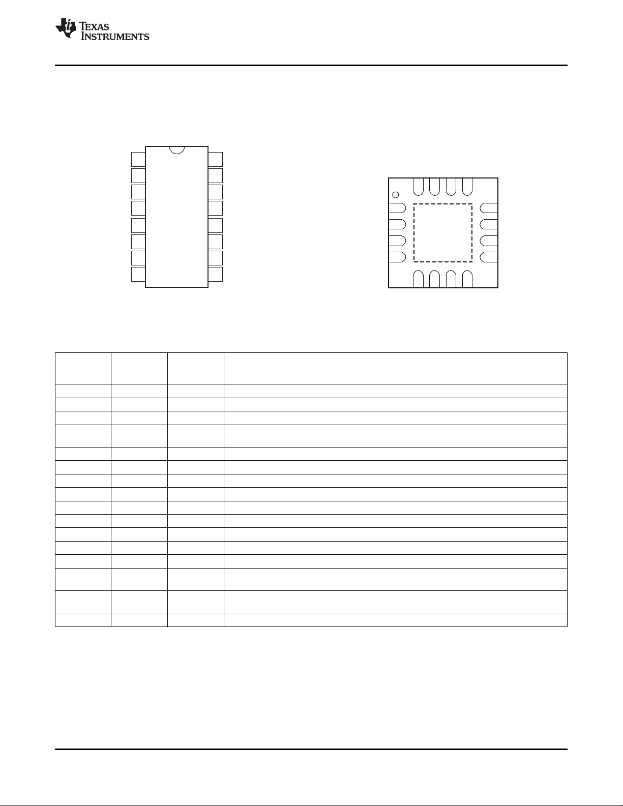
PIN CONFIGURATIONS
TMP512
space
D PACKAGE
SO-14
(TOP VIEW)
TMP512: PIN DESCRIPTIONS
PIN NO. NAME DESCRIPTION
1 Filter C Subregulator output and filter capacitor pin.
2 V+ Positive supply voltage (3V to 26V) See Figure 20.
3 V
4 V
IN+
IN-
5 SDA Serial bus data line for SMBus, open-drain; requires pull-up resistor.
6 SCL Serial bus clock line for SMBus, open-drain; requires pull-up resistor.
7 A0 Address pin
8 DXP1 Channel 1 positive connection to remote temperature sensor.
9 DXN1 Channel 1 negative connection to remote temperature sensor.
10 DXP2 Channel 2 positive connection to remote temperature sensor.
11 DXN2 Channel 2 negative connection to remote temperature sensor.
12 GPIO
13 ALERT Open-drain SMBus alert output. Controlled in SMBus Alert Mask Register. Default state is disabled.
14 GND Ground
Positive differential shunt voltage. Connect to positive side of shunt resistor.
Negative differential shunt voltage. Connect to negative side of shunt resistor. Bus voltage is measured
from this pin to ground.
General-purpose, user-programmable input/output. Totem-pole output. Connect to ground or supply
through a resistor if not used. Default state is as an input.
www.ti.com
6 Submit Documentation Feedback Copyright © 2010, Texas Instruments Incorporated
Product Folder Link(s): TMP512 TMP513
Page 7
1
2
3
4
5
6
7
8
16
15
14
13
12
11
10
9
Filter C
V+
V
IN+
V
IN-
SDA
SCL
A0
DXP1
GND
ALERT
GPIO
DXN3
DXP3
DXN2
DXP2
DXN1
TMP513
V
IN+
V
IN-
SDA
SCL
GPIO
DXN3
DXP3
DXN2
12
11
10
9
FilterC
1
2
3
4
5
6
7
8
13
14
15
16
A0
DXP1
DXN1
DXP2
ALERT
GND
V+
TMP513
TMP512
TMP513
www.ti.com
TMP513
space
D PACKAGE
SO-16
(TOP VIEW)
(1) Product preview device.
TMP513: PIN DESCRIPTIONS
D PACKAGE PACKAGE
SO-16 QFN-16 NAME DESCRIPTION
1 15 Filter C Subregulator output and filter capacitor pin.
2 16 V+ Positive supply voltage (3V to 26V) See Figure 20.
3 1 V
4 2 V
5 3 SDA Serial bus data line for SMBus, open-drain; requires pull-up resistor.
6 4 SCL Serial bus clock line for SMBus, open-drain; requires pull-up resistor.
7 5 A0 Address pin
8 6 DXP1 Channel 1 positive connection to remote temperature sensor.
9 7 DXN1 Channel 1 negative connection to remote temperature sensor.
10 8 DXP2 Channel 2 positive connection to remote temperature sensor.
11 9 DXN2 Channel 2 negative connection to remote temperature sensor.
12 10 DXP3 Channel 3 positive connection to remote temperature sensor.
13 11 DXN3 Channel 3 negative connection to remote temperature sensor.
14 12 GPIO
15 13 ALERT
16 14 GND Ground
RSA
IN+
IN-
Positive differential shunt voltage. Connect to positive side of shunt resistor.
Negative differential shunt voltage. Connect to negative side of shunt resistor. Bus voltage is
measured from this pin to ground.
General-purpose, user-programmable input/output. Totem-pole output. Connect to ground or
supply through a resistor if not used. Default state is as an input.
Open-drain SMBus alert output. Controlled in SMBus Alert Mask Register. Default state is
disabled.
RSA PACKAGE
SBOS491 –JUNE 2010
(1)
QFN-16
(TOP VIEW)
Product Folder Link(s): TMP512 TMP513
Copyright © 2010, Texas Instruments Incorporated Submit Documentation Feedback 7
Page 8
-40 -25 0 25 50
75
100 125
6
5
4
3
2
1
0
1
2
3
4
5
6
-
-
-
-
-
-
Remote Temperature Error ( C)?
Ambient Temperature ( C)?
34 Units Shown
10
100
1k
10k 100k
1M
Gain(dB)
InputFrequency(Hz)
0
10
20
30
40
50
60
70
80
90
100
-
-
-
-
-
-
-
-
-
-
-40
-25
0
25 50
75 100
Local Temperature Error ( C)°
Ambient Temperature ( C)°
125
14 Units Shown
2.0
1.5
1.0
0.5
0
0.5
1.0
1.5
2.0
-
-
-
-
-40
-25
0
25 50
75 100
Offset( V)m
Temperature( C)°
125
15
10
5
0
5
10
15
-
-
-
40mVRange
80mVRange
160mVRange
320mVRange
-40
-25
0
25 50
75 100
GainError(m%)
Temperature( C)°
125
250
200
150
100
50
0
50
100--
320mVRange
160mVRange
80mVRange
40mVRange
-40
-25
0
25 50
75 100
Offset (mV)
Temperature ( C)°
125
32V Range
16V Range
35
30
25
20
15
10
5
0
5
10
15
-
-
-
TMP512
TMP513
SBOS491 –JUNE 2010
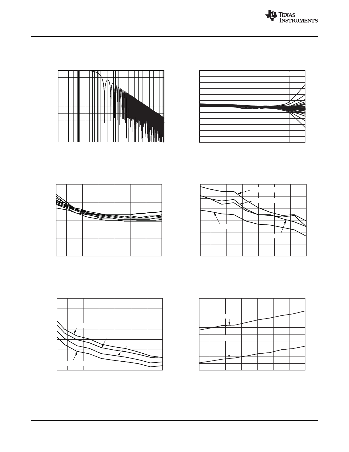
At TA= +25°C, V+ = 12V, V
LOCAL TEMPERATURE ERROR vs TEMPERATURE SHUNT OFFSET vs TEMPERATURE
www.ti.com
TYPICAL CHARACTERISTICS: V+ = +12V
= (V
– V
SENSE
IN+
FREQUENCY RESPONSE REMOTE TEMPERATURE ERROR vs TEMPERATURE
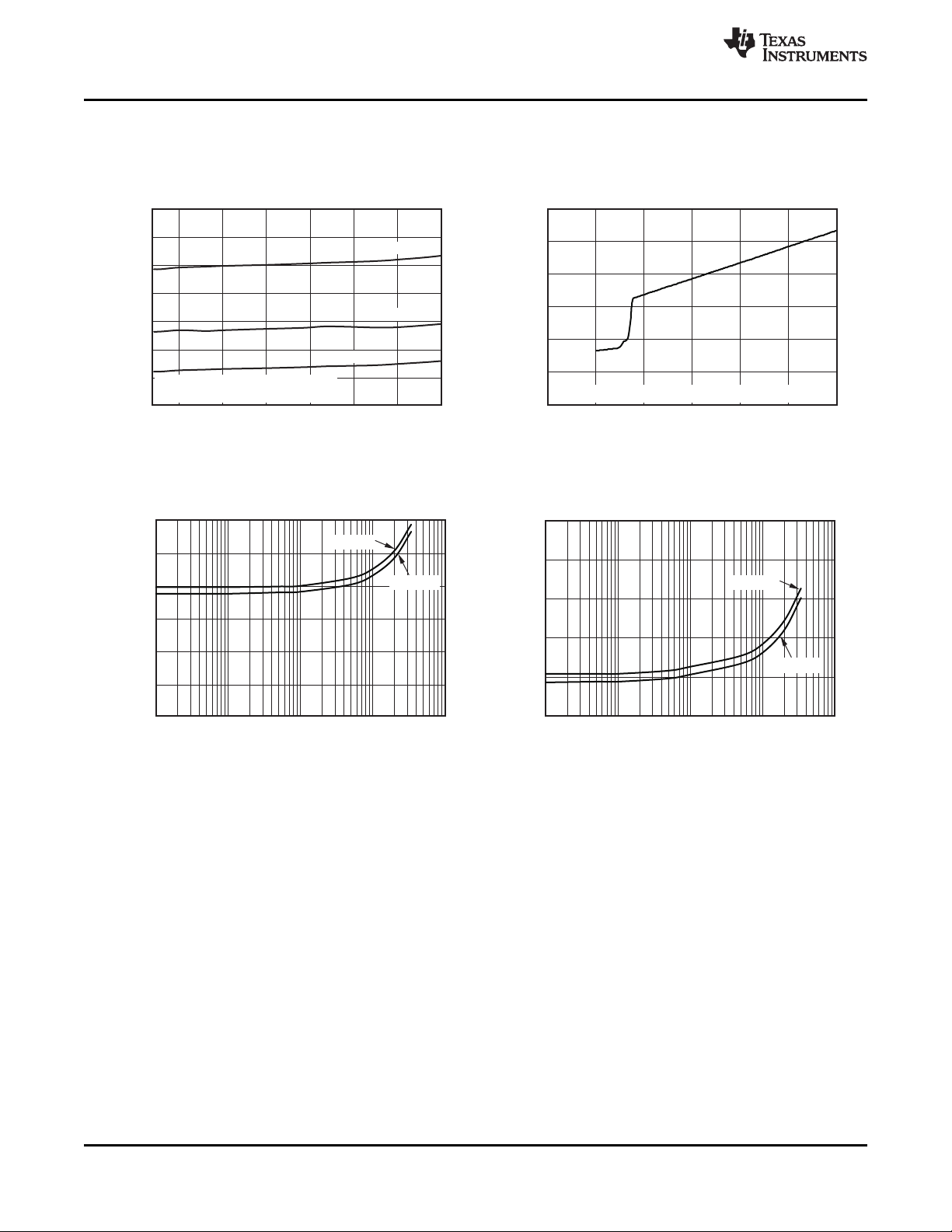
Figure 1. Figure 2.
) = 32mV, PGA = ÷ 1, and BRNG = 1, unless otherwise noted.
IN–
8 Submit Documentation Feedback Copyright © 2010, Texas Instruments Incorporated
Figure 3. Figure 4.
SHUNT GAIN ERROR vs TEMPERATURE BUS VOLTAGE OFFSET vs TEMPERATURE
Figure 5. Figure 6.
Product Folder Link(s): TMP512 TMP513
Page 9
20
15
10
5
0
-5
-10
-15
-20
-0.4
-0.3
-0.2
-0.1 0
0.1 0.2 0.3
INL( V)m
InputVoltage(V)
0.4
-40
-25
0
25 50
75 100
Gain Error (m%)
Temperature ( C)°
125
250
200
150
100
50
0
50
100--
32V Range
16V Range
0
5
10
15 20
25
Input Currents (mA)
V Voltage (V)
IN-
30
2.0
1.5
1.0
0.5
0
0.5
1.0
1.5
-
-
-
V+ = 5.5V
V+ 5.5V=
V+ = 3V
V+ 3V=
Current into V
IN-
Current into V
IN+
-40
-25
0
25 50
75 100
I (mA)
Q
Temperature ( C)°
125
V+ = 5.5V
V+ = 12V
V+ = 3V
1.4
1.2
1.0
0.8
0.6
0.4
0.2
0
TMP512
TMP513
www.ti.com
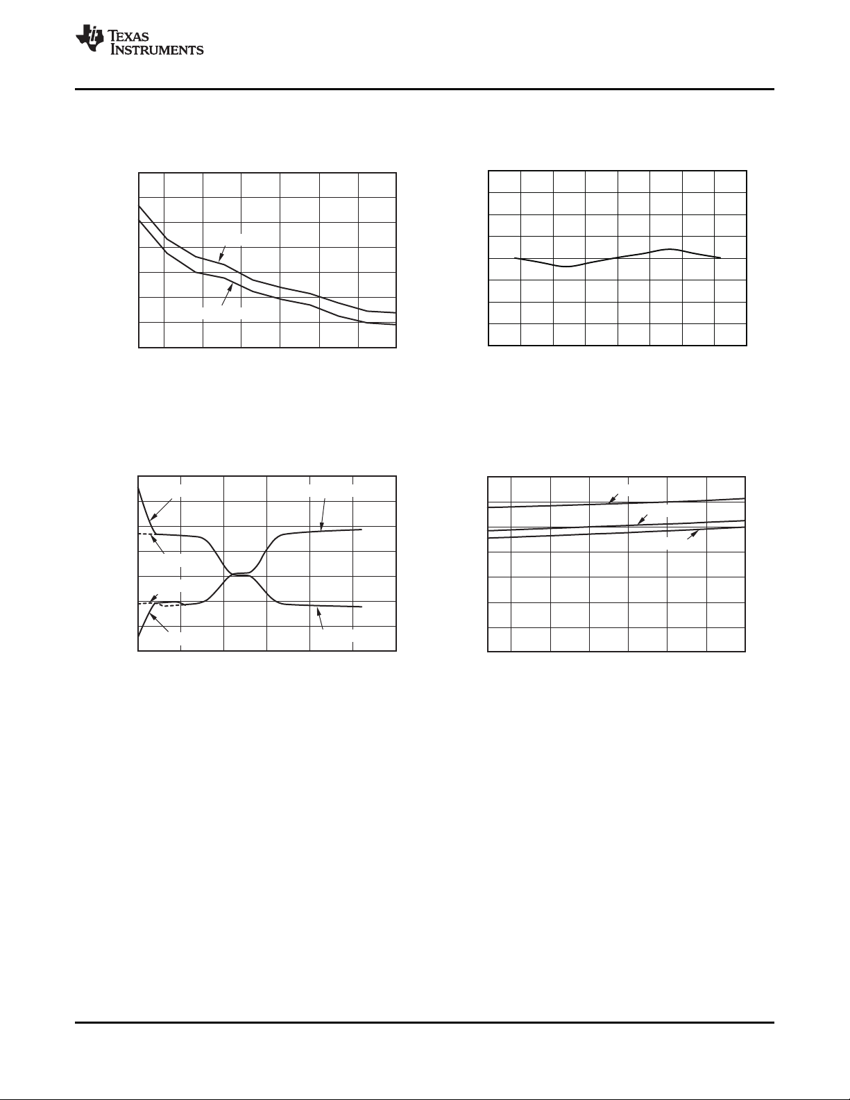
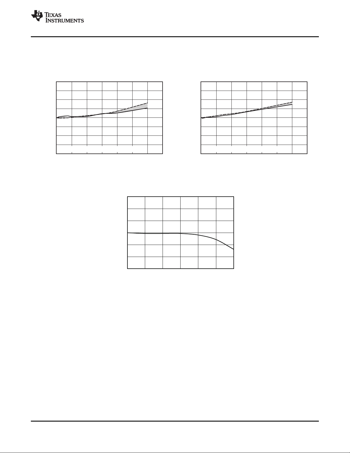
At TA= +25°C, V+ = 12V, V
BUS GAIN ERROR vs TEMPERATURE INTEGRAL NONLINEARITY vs INPUT VOLTAGE
INPUT CURRENTS WITH LARGE DIFFERENTIAL
(V
IN+
TYPICAL CHARACTERISTICS: V+ = +12V (continued)
= (V
– V
SENSE
IN+
Figure 7. Figure 8.
VOLTAGES
at 12V, Sweep of V
) = 32mV, PGA = ÷ 1, and BRNG = 1, unless otherwise noted.
IN–
) ACTIVE IQvs TEMPERATURE
IN–
SBOS491 –JUNE 2010
Copyright © 2010, Texas Instruments Incorporated Submit Documentation Feedback 9
Figure 9. Figure 10.
Product Folder Link(s): TMP512 TMP513
Page 10
I ( )
Q
mA
V (SV)
4.53.0 3.5 4.0 5.55.02.5
120
100
80
60
40
20
0
Note: Shutdown I vs V is for Subregulator Configuration 3
Q S
-40
-25
0
25
125
I ( A)m
Q
Temperature ( C)°
V+ = 5.5V
V+ = 12V
V+ = 3V
50 75 100
140
120
100
80
60
40
20
0
Note: Shutdown I vs Temperature is
for Subregulator Configurations 1 and 2
Q
1k
10k
100k
1M
10M
I ( A)m
Q
SCL Frequency (Hz)
V+ = 12V
V+ = 3.3V
1100
1050
1000
950
900
850
800
1k
10k
100k
1M
10M
I ( A)m
Q
SCL Frequency (Hz)
250
200
150
100
50
0
V+ = 12V
V+ = 3.3V
TMP512
TMP513
SBOS491 –JUNE 2010
At TA= +25°C, V+ = 12V, V
SHUTDOWN IQvs TEMPERATURE SUPPLY VOLTAGE
ACTIVE IQvs TWO-WIRE CLOCK FREQUENCY SHUTDOWN IQvs TWO-WIRE CLOCK FREQUENCY
TYPICAL CHARACTERISTICS: V+ = +12V (continued)
= (V
– V
SENSE
IN+
Figure 11. Figure 12.
) = 32mV, PGA = ÷ 1, and BRNG = 1, unless otherwise noted.
IN–
SHUTDOWN IQvs
www.ti.com
10 Submit Documentation Feedback Copyright © 2010, Texas Instruments Incorporated
Figure 13. Figure 14.
Product Folder Link(s): TMP512 TMP513
Page 11
Remote Temperature Error ( )°C
R ( W )
S
2.0
1.5
1.0
0.5
0
-0.5
-1.0
-1.5
-2.0
0 3500500 1000 1500 2000 2500 3000
Note: For all three subregulator configurations.
Remote Temperature Error ( )°C
R ( W )
S
2.0
1.5
1.0
0.5
0
-0.5
-1.0
-1.5
-2.0
0 3500500 1000 1500 2000 2500 3000
Note: For all three subregulator configurations.
3
2
1
0
-1
-2
-3
Capacitance(nF)
0 0.5 1.0 1.5 2.0 2.5 3.0
RemoteTemperatureError( C)°
TMP512
TMP513
www.ti.com
At TA= +25°C, V+ = 12V, V
REMOTE TEMPERATURE ERROR vs SERIES REMOTE TEMPERATURE ERROR vs SERIES
(Diode-Connected Transistor, 2N3906 PNP) (GND Collector-Connected Transistor, 2N3906 PNP)
TYPICAL CHARACTERISTICS: V+ = +12V (continued)
= (V
– V
SENSE
IN+
RESISTANCE RESISTANCE
Figure 15. Figure 16.
) = 32mV, PGA = ÷ 1, and BRNG = 1, unless otherwise noted.
IN–
REMOTE TEMPERATURE ERROR
vs DIFFERENTIAL CAPACITANCE
SBOS491 –JUNE 2010
Copyright © 2010, Texas Instruments Incorporated Submit Documentation Feedback 11
Figure 17.
Product Folder Link(s): TMP512 TMP513
Page 12
(b) Diode-Connected Transistor
(a) GND Collector-Connected Transistor
DXP
DXN
R
S1
(1)
R
S2
(1)
DXP
DXN
R
S1
(1)
R
S2
(1)
(b) Diode-ConnectedTransistor
(a) GNDCollector-ConnectedTransistor
DXP
DXN
C
DIFF
(1)
DXP
DXN
C
DIFF
(1)
TMP512
TMP513
SBOS491 –JUNE 2010
PARAMETRIC MEASUREMENT INFORMATION
TYPICAL CONNECTIONS
SERIES RESISTANCE CONFIGURATION
(1) RS1+ RS2should be less than 1kΩ; see Filtering section.
DIFFERENTIAL CAPACITANCE CONFIGURATION
www.ti.com
Figure 18.
(1) C
12 Submit Documentation Feedback Copyright © 2010, Texas Instruments Incorporated
should be less than 2200pF; see Filtering section.
DIFF
Figure 19.
Product Folder Link(s): TMP512 TMP513
Page 13
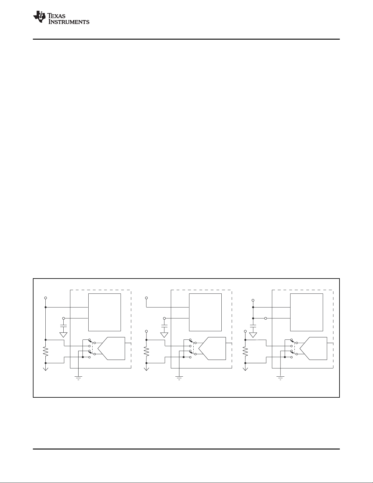
Configuration 1 Configuration 2 Configuration 3
GND
ADC
Subregulator
3.3V
Subregulator
3.3V
V+ = 4.5V to 26V
Filter C
Load
470nF
Bus Voltage Range = 4.5V to 26V
Shunt
R
SHUNT
V
IN+
V
IN-
GND
ADC
V+ = 4.5V to 26V
Load
Filter C
470nF
Bus Voltage Range = 0V to 26V
Shunt
R
SHUNT
V
IN+
V
IN-
GND
ADC
Subregulator
3.3V
V+ = 3V to 5.5V
Load
Filter C
100nF
Bus Voltage Range = 0V to 26V
Shunt
R
SHUNT
V
IN+
V
IN-
TMP512
TMP513
www.ti.com
SBOS491 –JUNE 2010
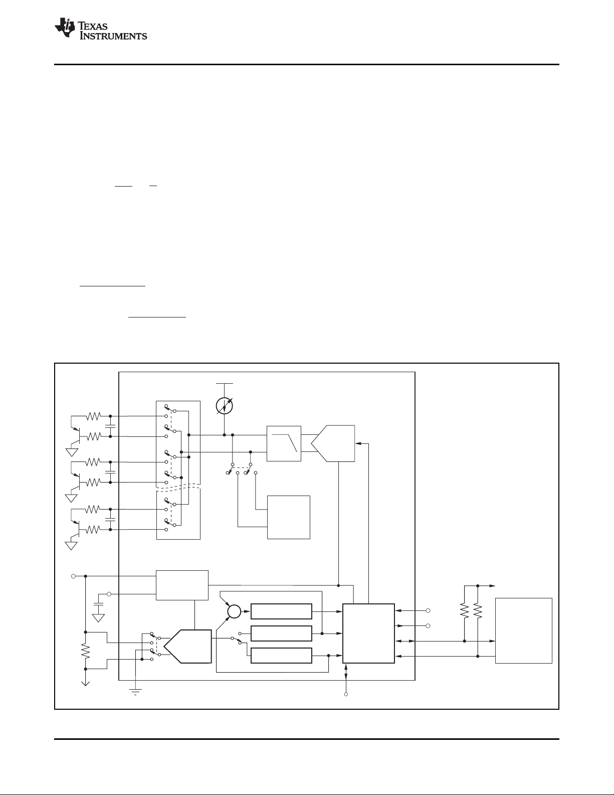
APPLICATION INFORMATION
between the two systems is being addressed. Two
DESCRIPTION
The TMP512/13 are digital temperature sensors with
a digital current-shunt monitor that combine a local
die temperature measurement channel and remote
junction temperature measurement channels: two for
the TMP512 and three for the TMP513. The
TMP512/13 contain multiple registers for holding The subregulator can be configured to three different
configuration information, temperature, and voltage modes of operation. Each mode has its advantage
measurement results. These devices provide digital and limitation. Figure 20 shows the three
current, voltage, and power readings necessary for configuration arrangements. The minimum
accurate decision-making in precisely-controlled capacitance on the Filter C pin for Configurations 1
systems. Programmable registers allow flexible and 2 is 470nF. The minimum capacitance on the
configuration for setting warning limits, measurement Filter C pin for Configuration 3 is 100nF.
resolution, and continuous-versus-triggered
operation. Detailed register information appears at
the end of this data sheet, beginning with Table 3.
For proper remote temperature sensing operation, the V+ supply range of 4.5V to 26V connected to the
TMP512 requires transistors connected between shunt voltage, the bus voltage range cannot go to
DXP1 and DXN1 and between DXP2 and DXN2, and zero and is limited to 4.5V to 26V.
for the TMP513, between DXP3 and DXN3 as well.
Unused channels on the TMP512/13 must be
connected to GND.
The TMP512/13 offer compatibility with two-wire and is not limited to 4.5V as in Configuration 1.
SMBus interfaces. The two-wire and SMBus
protocols are essentially compatible with each other.
Two-wire is used throughout this data sheet, with
SMBus being specified only when a difference
bi-directional lines, SCL and SDA, connect the
TMP512/13 to the bus. SDA is an open-drain
connection. See Figure 21 for a typical application
circuit.
SUBREGULATOR
Configuration 1 has V+ and V
supplies the subregulator, which in turn supplies the
3.3V to the Filter C pin and the internal die. With the
Configuration 2 has V+ to the subregulator without
any other connections. Under this configuration, the
bus voltage range can go from 0V to 26V, because it
Configuration 3 has the subregulator V+ and Filter C
pins shorted together. V+ is limited to 3V to 5.5V
because the Filter C pin supplies the internal die; it
cannot exceed this voltage range. The bus voltage
range can go from 0V to 26V, because it is not limited
to 4.5V as in Configuration 1.
tied together. V+
IN+
Copyright © 2010, Texas Instruments Incorporated Submit Documentation Feedback 13
Figure 20. Typical Subregulator Configurations
Product Folder Link(s): TMP512 TMP513
Page 14

TMP512
TMP513
SBOS491 –JUNE 2010
www.ti.com
SERIES RESISTANCE CANCELLATION Local Temperature Result Register and the Remote
Series resistance in an application circuit that typically
results from printed circuit board (PCB) trace
resistance and remote line length is automatically
cancelled by the TMP512/13, preventing what would
otherwise result in a temperature offset. A total of up
to 3kΩ of series line resistance is cancelled by the
TMP512/13, eliminating the need for additional
characterization and temperature offset correction.
See the Remote Temperature Error vs Series
Resistance typical characteristic curves (Figure 15 )
for details on the effects of series resistance and
power-supply voltage on sensed remote temperature
error.
Temperature Result Registers. Note that byte 1 is the
most significant byte, followed by byte 2, the least
significant byte. The first 13 bits are used to indicate
temperature. The least significant byte does not have
to be read if that information is not needed. The data
format for temperature is summarized in Table 10.
One LSB equals 0.0625°C. Negative numbers are
represented in binary twos complement format.
Following power-up or reset, the Temperature
Register will read 0°C until the first conversion is
complete. Unused bits in the Temperature Register
always read '0'.
REGISTER INFORMATION
DIFFERENTIAL INPUT CAPACITANCE The TMP512/13 contain multiple registers for holding
The TMP512/13 can tolerate differential input
capacitance of up to 2200pF with minimal change in
temperature error. The effect of capacitance on
sensed remote temperature error is illustrated in
Figure 16, Remote Temperature Error vs Differential
Capacitance. See the Filtering section for suggested
component values where filtering unwanted coupled
signals is needed.
configuration information, temperature and voltage
measurement results, and status information. These
registers are described in Table 3.
POINTER REGISTER
The 8-bit Pointer Register is used to address a given
data register. The Pointer Register identifies which of
the data registers should respond to a read or write
command on the two-wire bus. This register is set
TEMPERATURE MEASUREMENT DATA with every write command. A write command must be
Temperature measurement data may be taken over
an operating range of –40°C to +125°C for both local
and remote locations.
The Temperature Register of the TMP512/13 is
configured as a 13-bit, read-only register that stores
the output of the most recent conversion. Two bytes
must be read to obtain data, and are described in the
issued to set the proper value in the Pointer Register
before executing a read command. Table 3 describes
the pointer address of the TMP512/13 registers. The
power-on reset (POR) value of the Pointer Register is
00h (0000 0000b).
14 Submit Documentation Feedback Copyright © 2010, Texas Instruments Incorporated
Product Folder Link(s): TMP512 TMP513
Page 15
V V =-
BE2 BE1
nkT
q
I
I
2
1
(
(
In
n =
eff
1.008 300
(300 N )-
ADJUST
´
N 300
ADJUST
-=
300 1.008
n
eff
´
(
(
´
Power Register
Current Register
Two-Wire
Interface
Voltage Register
ADC
GND
GPIO
DXP1
DXN1
DXP2
DXN2
ADC
Low-Pass Filter
MUX
DXP3
DXN3
V
IN+
V
IN-
Current
Shunt
Load
Filter C
V+
Subregulator
3.3V
Internal
Diode
Temperature
Sensor
A0
ALERT
SDA
SCL
SMBus
Controller
3.3V Supply
TMP512
TMP513
TMP512
TMP513
www.ti.com
SBOS491 –JUNE 2010
n-FACTOR CORRECTION REGISTER twos-complement format, yielding an effective data
The TMP512/13 allow for a different n-factor value to
be used for converting remote channel
measurements to temperature. The remote channel
uses sequential current excitation to extract a
differential VBEvoltage measurement to determine
the temperature of the remote transistor. Equation 1
describes this voltage and temperature.
(1)
The value n in Equation 1 is a characteristic of the
particular transistor used for the remote channel. The
power-on reset value for the TMP512/13 is n = 1.008.
The value in the n-Factor Correction Register may be
used to adjust the effective n-factor according to
Equation 2 and Equation 3.
(2)
(3)
The n-factor value must be stored in Acknowledge and pulling SDA LOW.
range from –128 to +127. The n-factor value may be
written to and read from pointer address 16h for
remote channel 1, pointer address 17h for remote
channel 2, and pointer address 18h for remote
channel 3. The register power-on reset value is 00h,
thus having no effect unless the register is written to.
BUS OVERVIEW
The device that initiates the transfer is called a
master, and the devices controlled by the master are
slaves. The bus must be controlled by a master
device that generates the serial clock (SCL), controls
the bus access, and generates START and STOP
conditions.
To address a specific device, the master initiates a
START condition by pulling the data signal line (SDA)
from a HIGH to a LOW logic level while SCL is HIGH.
All slaves on the bus shift in the slave address byte
on the rising edge of SCL, with the last bit indicating
whether a read or write operation is intended. During
the ninth clock pulse, the slave being addressed
responds to the master by generating an
Copyright © 2010, Texas Instruments Incorporated Submit Documentation Feedback 15
Figure 21. Typical Application Circuit
Product Folder Link(s): TMP512 TMP513
Page 16

TMP512
TMP513
SBOS491 –JUNE 2010
www.ti.com
Data transfer is then initiated and eight bits of data WRITING TO/READING FROM THE
are sent, followed by an Acknowledge bit. During TMP512/13
data transfer, SDA must remain stable while SCL is
HIGH. Any change in SDA while SCL is HIGH is
interpreted as a START or STOP condition.
Accessing a particular register on the TMP512/13 is
accomplished by writing the appropriate value to the
register pointer. Refer to Table 3 for a complete list of
Once all data have been transferred, the master registers and corresponding addresses. The value for
generates a STOP condition, indicated by pulling the register pointer as shown in Figure 24 is the first
SDA from LOW to HIGH while SCL is HIGH. The byte transferred after the slave address byte with the
TMP512/13 includes a 28ms timeout on its interface R/W bit LOW. Every write operation to the
to prevent locking up an SMBus. TMP512/13 requires a value for the register pointer.
SERIAL BUS ADDRESS
To communicate with the TMP512/13, the master
must first address slave devices via a slave address
byte. The slave address byte consists of seven
address bits, and a direction bit indicating the intent
of executing a read or write operation.
The TMP512/13 feature an address pin to allow up to
four devices to be addressed on a single bus. Table 1
describes the pin logic levels used to properly
connect up to four devices. The state of the A0 pin is
sampled on every bus communication and should be
set before any activity on the interface occurs. The
address pin is read at the start of each
communication event.
Writing to a register begins with the first byte
transmitted by the master. This byte is the slave
address, with the R/W bit LOW. The TMP512/13 then
acknowledge receipt of a valid address. The next
byte transmitted by the master is the address of the
register to which data will be written. This register
address value updates the register pointer to the
desired register. The next two bytes are written to the
register addressed by the register pointer. The
TMP512/13 acknowledge receipt of each data byte.
The master may terminate data transfer by
generating a START or STOP condition.
When reading from the TMP512/13, the last value
stored in the register pointer by a write operation
determines which register is read during a read
operation. To change the register pointer for a read
Table 1. TMP512/13 Address Pins and
operation, a new value must be written to the register
Slave Addresses pointer. This write is accomplished by issuing a slave
DEVICE TWO-WIRE
ADDRESS A0 PIN CONNECTION
1011100 Ground
1011101 V+
1011110 SDA
1011111 SCL
address byte with the R/W bit LOW, followed by the
register pointer byte. No additional data are required.
The master then generates a START condition and
sends the slave address byte with the R/W bit HIGH
to initiate the read command. The next byte is
transmitted by the slave and is the most significant
byte of the register indicated by the register pointer.
This byte is followed by an Acknowledge from the
SERIAL INTERFACE
master; then the slave transmits the least significant
byte. The master acknowledges receipt of the data
The TMP512/13 operate only as slave devices on the byte. The master may terminate data transfer by
two-wire bus and SMBus. SCL is an input only, and generating a Not-Acknowledge after receiving any
TMP512/13 cannot drive it. Connections to the bus data byte, or generating a START or STOP condition.
are made via the open-drain I/O lines SDA and SCL. If repeated reads from the same register are desired,
The SDA and SCL pins feature integrated spike it is not necessary to continually send the register
suppression filters and Schmitt triggers to minimize pointer bytes; the TMP512/13 retain the register
the effects of input spikes and bus noise. The pointer value until it is changed by the next write
TMP512/13 support the transmission protocol for fast operation.
(1kHz to 400kHz) and high-speed (1kHz to 3.4MHz)
modes. All data bytes are transmitted MSB first.
Figure 22 and Figure 23 show read and write
operation timing diagrams, respectively. Note that
register bytes are sent most-significant byte first,
followed by the least significant byte. See Figure 25
for an illustration of a typical register pointer
configuration.
16 Submit Documentation Feedback Copyright © 2010, Texas Instruments Incorporated
Product Folder Link(s): TMP512 TMP513
Page 17
Frame1Two-WireSlaveAddressByte
(1)
Frame2DataMSByte
(2)
1
StartBy
Master
ACKBy
TMP512/TMP513
ACKBy
Master
From
TMP512/TMP513
1 9 1
9
SDA
SCL
0 1 1 R/
W D15 D14 D13 D12 D11 D10 D9 D8
1 A1 A0
Frame3DataLSByte
(2)
StopNoACKBy
(3)
Master
From
TMP512/TMP513
1
9
D7 D6 D5 D4 D3 D2 D1 D0
NOTES:(1)ThevalueoftheSlaveAddressByteisdeterminedbythesettingsoftheA0pin.
RefertoTable1.
(2)Readdataisfromthelastregisterpointerlocation.Ifanewregisterisdesired,theregister
pointermustbeupdated.SeeFigure23.
(3)ACKbyMastercanalsobesent.
Frame1Two-WireSlaveAddressByte
(1)
Frame2RegisterPointerByte
StartBy
Master
ACKBy
TMP512/TMP513
ACKBy
TMP512/TMP513
1 9 1
ACKBy
TMP512/TMP513
1
D15 D14 D13 D12 D11 D10 D9 D8
9
9
SDA
SCL
1 0 1 1 1
A1 A0 R/W P7 P6 P5 P4 P3 P2 P1 P0
NOTE(1):ThevalueoftheSlaveAddressByteisdeterminedbythesettingsoftheA0pin.RefertoTable1.
Frame4DataLSByteFrame3DataMSByte
ACKBy
TMP512/TMP513
StopBy
Master
1
D7 D6 D5 D4 D3 D2 D1 D0
9
TMP512
TMP513
www.ti.com
SBOS491 –JUNE 2010
Figure 22. Timing Diagram for Write Word Format
Copyright © 2010, Texas Instruments Incorporated Submit Documentation Feedback 17
Product Folder Link(s): TMP512 TMP513
Figure 23. Timing Diagram for Read Word Format
Page 18

Frame1SMBusALERTResponseAddressByte Frame2SlaveAddressByte
(1)
StartBy
Master
ACKBy
TMP512/TMP513
From
TMP512/TMP513
NACKBy
Master
StopBy
Master
1 9 1
9
SDA
SCL
ALERT
0 0 0 1 1 0 0 R/
W 1 0 1 1 1 A1 A0
0
NOTE(1):ThevalueoftheSlaveAddressByteisdeterminedbythesettingsoftheA0pin.RefertoTable1.
Frame1Two-WireSlaveAddressByte
(1)
Frame2RegisterPointerByte
1
StartBy
Master
ACKBy
TMP512/TMP513
ACKBy
TMP512/TMP513
1 9 1 9
SDA
SCL
0 1 1 1 A1 A0 R/W P7 P6 P5 P4 P3 P2 P1 P0 Stop
¼
NOTE(1):ThevalueoftheSlaveAddressByteisdeterminedbythesettingsoftheA0pin.RefertoTable1.
TMP512
TMP513
SBOS491 –JUNE 2010
www.ti.com
Figure 24. Timing Diagram for SMBus ALERT
Figure 25. Typical Register Pointer Set
18 Submit Documentation Feedback Copyright © 2010, Texas Instruments Incorporated
Product Folder Link(s): TMP512 TMP513
Page 19

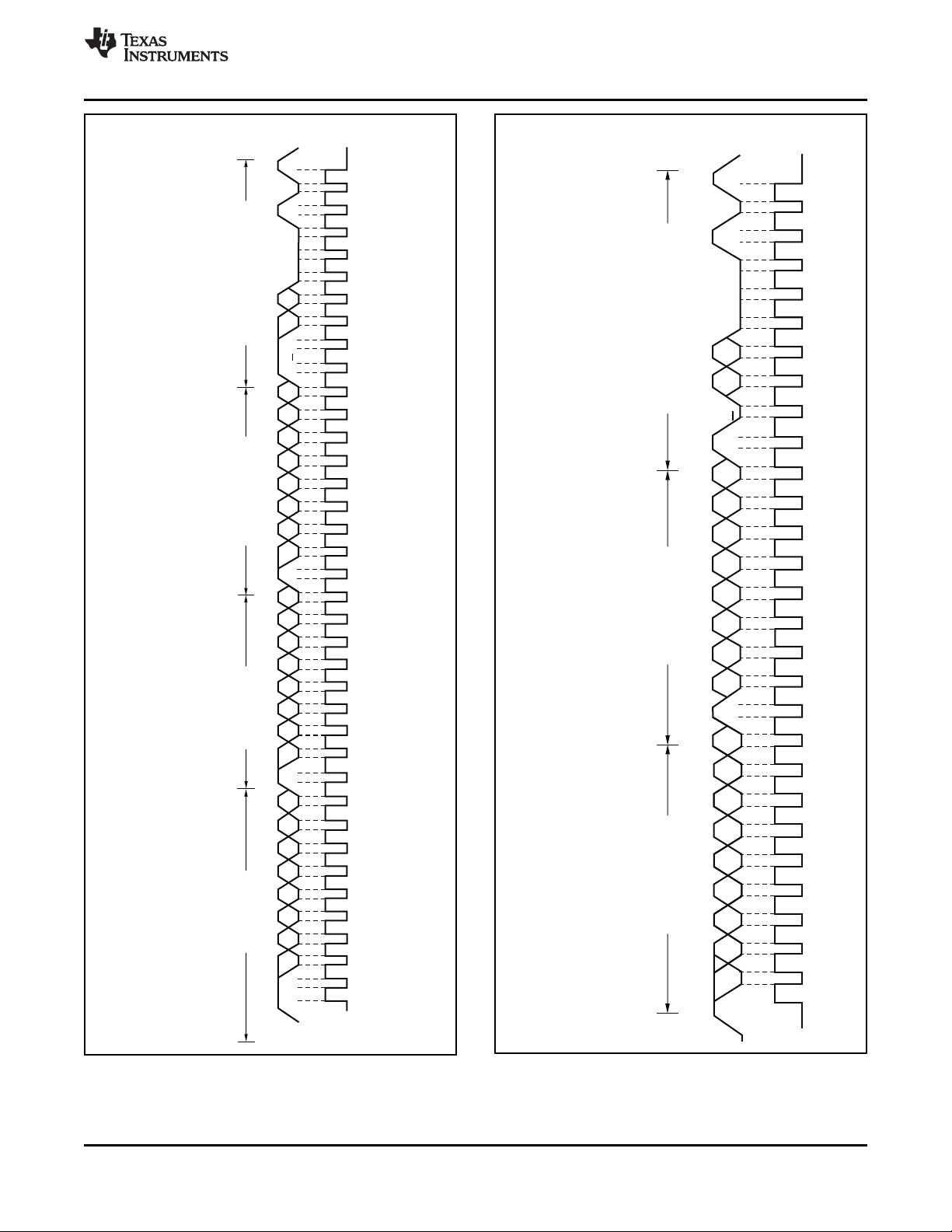
SCL
SDA
t
(LOW)
t
R
t
F
t
(HDSTA)
t
(HDSTA)
t
(HDDAT)
t
(BUF)
t
(SUDAT)
t
(HIGH)
t
(SUSTA)
t
(SUSTO)
P S S P
TMP512
TMP513
www.ti.com
SBOS491 –JUNE 2010
TIMING DIAGRAMS Data Transfer: The number of data bytes transferred
Figure 26 describes the timing operations on the
TMP512/13. Parameters for Figure 26 are defined in
Table 2. Bus definitions are:
Bus Idle: Both SDA and SCL lines remain high.
Start Data Transfer: A change in the state of the
SDA line, from high to low, while the SCL line is high,
defines a START condition. Each data transfer
initiates with a START condition. Denoted as S in
Figure 26.
Stop Data Transfer: A change in the state of the
SDA line from low to high while the SCL line is high
defines a STOP condition. Each data transfer
terminates with a repeated START or STOP
condition. Denoted as P in Figure 26.
between a START and a STOP condition is not
limited and is determined by the master device. The
receiver acknowledges data transfer.
Acknowledge: Each receiving device, when
addressed, is obliged to generate an Acknowledge
bit. A device that acknowledges must pull down the
SDA line during the Acknowledge clock pulse in such
a way that the SDA line is stable low during the high
period of the Acknowledge clock pulse. Setup and
hold times must be taken into account. On a master
receive, data transfer termination can be signaled by
the master generating a Not-Acknowledge on the last
byte that has been transmitted by the slave.
Figure 26. Two-Wire Timing Diagram
Table 2. Timing Characteristics for Figure 26
FAST MODE HIGH-SPEED MODE
PARAMETER MIN MAX MIN MAX UNIT
SCL Operating Frequency f
Bus Free Time Between STOP and START Condition t
Hold time after repeated START condition. After this period, the first clock
is generated.
Repeated START Condition Setup Time t
STOP Condition Setup Time t
Data Hold Time t
Data Setup Time t
SCL Clock LOW Period t
SCL Clock HIGH Period t
Clock/Data Fall Time t
Clock/Data Rise Time t
for SCL ≤ 100kHz t
(SCL)
(BUF)
t
(HDSTA)
(SUSTA)
(SUSTO)
(HDDAT)
(SUDAT)
(LOW)
(HIGH)
(1) For cases with fall time of SCL less than 20ns and/or the rise or fall time of SDA less than 20ns, the hold time should be greater than
20ns.
(2) For cases with a fall time of SCL less than 10ns and/or the rise or fall time of SDA less than 10ns, the hold time should be greater than
10ns.
0.001 0.4 0.001 3.4 MHz
600 160 ns
100 100 ns
100 100 ns
100 100 ns
(1)
0
100 10 ns
1300 160 ns
600 60 ns
F
R
R
300 160 ns
300 160
1000
(2)
0
ns
ns
Copyright © 2010, Texas Instruments Incorporated Submit Documentation Feedback 19
Product Folder Link(s): TMP512 TMP513
Page 20

TMP512
TMP513
SBOS491 –JUNE 2010
www.ti.com
HIGH-SPEED MODE SENSOR FAULT
In order for the two-wire bus to operate at frequencies The TMP512/13 can sense an open circuit.
above 400kHz, the master device must issue a Short-circuit conditions return a value of –256°C. The
High-Speed mode (Hs-mode) master code (0000 detection circuitry consists of a voltage comparator
1xxx) as the first byte after a START condition to that trips when the voltage at DXP exceeds (V+) –
switch the bus to high-speed operation. The 0.6V (typical). The comparator output is continuously
TMP512/13 do not acknowledge this byte, but switch checked during a conversion. If a fault is detected,
the input filters on SDA and SCL and the output filter the OPEN bit (bit 0) in the temperature result register
on SDA to operate in Hs-mode, allowing transfers at is set to '1' and the rest of the register bits should be
up to 3.4MHz. After the Hs-mode master code has ignored.
been issued, the master transmits a START condition
to a two-wire slave address that initiates a data
transfer operation. The bus continues to operate in
Hs-mode until a STOP condition occurs on the bus.
Upon receiving the STOP condition, the TMP512/13
switch the input and output filters back to Fast mode
operation.
POWER-UP CONDITIONS
Power-up conditions apply to a software reset via the
RST bit (bit 15) in the Configuration Register, or the
two-wire bus General Call Reset. At device power up,
all Status bits are masked, and the SMBus Alert
function is disabled. All watchdog outputs default to
active low and transparent (non-latched) modes.
SHUTDOWN MODE
The TMP512/13 shutdown mode of operation allows the user flexibility to shut down the shunt/bus voltage measurement and the temperature measurement functions individually. TEMPERATURE AVERAGING
When not using the remote sensor with the
TMP512/13, the DXP and DXN inputs must be
connected together to prevent meaningless fault
warnings.
UNDERVOLTAGE LOCKOUT
The TMP512/13 sense when the power-supply
voltage has reached a minimum voltage level for the
ADC to function. The detection circuitry consists of a
voltage comparator that enables the ADC after the
power supply (V+) exceeds 2.7V (typical). The
comparator output is continuously checked during a
conversion. The TMP512/13 do not perform a
temperature conversion if the power supply is not
valid. The PVLD bit (see Status Register; Local
Temperature Reset Register; Remote Temperature
Reset 1, 2 and 3 Registers) of the individual
Local/Remote Temperature Result Registers are set
to '1' and the temperature result may be incorrect.
To shut down the shunt/bus voltage measurement The TMP512/13 average the input diode voltages
function immediately, set bits 2 through 0 in that determine the remote temperature by sampling
Configuration Register 1 (00h) to '000' respectively. multiple times throughout a conversion. The
To shut down the shunt/bus voltage measurement temperature result can be extracted from four
after the end of the current conversion, set bits 2 different VBEreadings and is sampled 600 times in
through 0 in Configuration Resister 1 (00h) to '100' 130ms (max). Each VBEvoltage is sampled 150 times
respectively. through integration capacitors that average the
To shut down the temperature measurement function
immediately, set bits 15 through 11 in Configuration
Register 2 (01h) to '00000' respectively. To shut
down the temperature measurement after the end of
the current conversion, set bit 15 in Configuration
Register 2 (01h) to '0'.
ONE-SHOT COMMAND
For the TMP512/13, when the temperature core is in
shutdown and the voltage core is in triggered mode, a
single conversion is started on all enabled channels
by writing a '1' to the OS bit in Configuration Register
1. This write operation starts one conversion; the
TMP512/13 returns to shutdown mode when that
conversion completes. At the end of the conversion,
the Conversion Ready flags (bit 6 and bit 5) in the
Status Register are set to indicate end of conversion.
results throughout the conversion time. A delta-sigma
(ΔΣ) modulator and digital filter integrate the V
voltages and create a sync filter averaging system. In
addition, a low-pass filter is present at the input of the
converter with a cutoff frequency of 65kHz. This
integrating topology offers superior noise immunity.
BE
FILTERING
Remote junction temperature sensors are usually
implemented in a noisy environment. Noise is
frequently generated by fast digital signals and if not
filtered properly will induce errors that can corrupt
temperature measurements. The TMP512/13 have a
built-in 65kHz filter on the inputs of DXP and DXN to
minimize the effects of noise. However, a bypass
capacitor placed differentially across the inputs of the
remote temperature sensor is recommended to make
the application more robust against unwanted
20 Submit Documentation Feedback Copyright © 2010, Texas Instruments Incorporated
Product Folder Link(s): TMP512 TMP513
Page 21

T
ERR
=
1.004 1.008
1.008
-
(
(
´ °273.15+100 C
)
)
T =1.48 C
ERR
°
T
ERR
=
n 1.008
1.008
-
(
(
´ °273.15+T( C)
TMP512
TMP513
www.ti.com
coupled signals. The value of this capacitor should be Where:
between 100pF and 1nF. Some applications attain
better overall accuracy with additional series
resistance; however, this increased accuracy is
application-specific. When series resistance is added,
the total value should not be greater than 3kΩ. If
filtering is needed, suggested component values are
100pF and 50Ω on each input; exact values are
application-specific.
n = ideality factor of remote temperature sensor.
T(°C) = actual temperature.
T
Degree delta is the same for °C and K.
For n = 1.004 and T(°C) = 100°C:
GENERAL CALL RESET
The TMP512/13 support reset via the two-wire
General Call address 00h (0000 0000b). The
TMP512/13 acknowledge the General Call address
and respond to the second byte. If the second byte is
06h (0000 0110b), the TMP512/13 execute a
software reset state to all TMP512/13 registers, and
abort any conversion in progress. The TMP512/13
take no action in response to other values in the
second byte.
REMOTE SENSING
The TMP512/13 are designed to be used with either
discrete transistors or substrate transistors built into
processor chips and ASICs. Either NPN or PNP
transistors can be used, as long as the base-emitter
junction is used as the remote temperature sense.
NPN transistors must be diode-connected. PNP
transistors can either be transistor- or
diode-connected, as Figure 18 and Figure 19 show.
Errors in remote temperature sensor readings are
typically the consequence of the ideality factor and
current excitation used by the TMP512/13 versus the
manufacturer-specified operating current for a given
transistor. Some manufacturers specify a high-level
and low-level current for the temperature-sensing
substrate transistors. The TMP512/13 use 6mA for
I
and 120mA for I
LOW
The ideality factor (n) is a measured characteristic of
a remote temperature sensor diode as compared to
an ideal diode. The TMP512/13 allow for different
n-factor values; see the n-Factor Correction Register
section.
The ideality factor for the TMP512/13 is trimmed to
be 1.008. For transistors that have an ideality factor
that does not match the TMP512/13, Equation 4 can
be used to calculate the temperature error. Note that
for the equation to be used correctly, actual
temperature (°C) must be converted to kelvins (K).
space
HIGH
.
(4)
If a discrete transistor is used as the remote
temperature sensor with the TMP512/13, the best
accuracy can be achieved by selecting the transistor
according to the following criteria:
1. Base-emitter voltage > 0.25V at 6mA, at the
highest sensed temperature.
2. Base-emitter voltage < 0.95V at 120mA, at the
lowest sensed temperature.
3. Base resistance < 100Ω.
4. Tight control of VBEcharacteristics indicated by
small variations in hFE(that is, 50 to 150).
Based on these criteria, two recommended
small-signal transistors are the 2N3904 (NPN) or
2N3906 (PNP).
BASIC ADC FUNCTIONS
The two analog inputs to the TMP512/13, V
V
, connect to a shunt resistor in the bus of interest.
IN–
The TMP512/13 are powered by an internal
subregulator, which has a typical output of 3.3V. The
bus being sensed can vary from 0V to 26V. There are
no special considerations for power-supply
sequencing (for example, a bus voltage can be
present with the supply voltage off, and vice-versa).
The TMP512/13 sense the small drop across the
shunt for shunt voltage, and sense the voltage with
respect to ground from V
Figure 27 for an illustration of this operation.
When the TMP512/13 are in the normal operating
mode (that is, MODE bits of Configuration Register 1
are set to '111'), the devices continuously convert the
shunt voltage up to the number set in the shunt
voltage averaging function (Configuration Register 1,
SADC bits). The devices then convert the bus voltage
up to the number set in the bus voltage averaging
(Configuration Register 1, BADC bits). The Mode
control in Configuration Register 1 also permits
selecting modes to convert only voltage or current,
either continuously or in response to a two-wire
command.
SBOS491 –JUNE 2010
= error in TMP512/13 because n ≠ 1.008.
ERR
for the bus voltage. See
IN–
IN+
(5)
and
Copyright © 2010, Texas Instruments Incorporated Submit Documentation Feedback 21
Product Folder Link(s): TMP512 TMP513
Page 22

´
Power Register
Current Register
Two-Wire
Interface
Voltage Register
ADC
GPIO
GND
DXP1
DXN1
DXP2
DXN2
ADC
Low-Pass Filter
MUX
DXP3
DXN3
V
IN+
V
IN-
Current
Shunt
Load
Filter C
V+
Subregulator
3.3V
Internal
Diode
Temperature
Sensor
A0
ALERT
SDA
SCL
SMBus
Controller
3.3V Supply
TMP512
TMP513
V = V -
SHUNT IN+VIN-
Typically < 50mV
V =
BUS
GND-V
IN-
Range of 0V to 26V
Typical Application: 12V
TMP512
TMP513
SBOS491 –JUNE 2010
www.ti.com
Figure 27. TMP512/13 Configured for Shunt and Bus Voltage Measurement
All current and power calculations are performed in
the background and do not contribute to conversion
time; conversion times shown in the Electrical
Characteristics table can be used to determine the
actual conversion time.
Power-Down mode reduces the quiescent current
and turns off current into the TMP512/13 inputs,
avoiding any supply drain. Full recovery from
Power-Down requires 40ms. ADC Off mode (set by
Configuration Register 1, MODE bits) stops all
conversions.
Although the TMP512/13 can be read at any time,
and the data from the last conversion remain
available, the Conversion Ready bit and the
Conversion Ready Temperature bit (Status Register,
CVR and CRT) are provided to help co-ordinate
one-shot or triggered conversions. The Conversion
Ready bit and the Conversion Ready Temperature bit
are set after all conversions, averaging, and
multiplication operations are complete.
The Conversion Ready bit and the Conversion Ready
Temperature bit clear when reading the Status
Register or triggering a single-shot conversion.
POWER MEASUREMENT
Current and bus voltage are converted at different
points in time, depending on the resolution and
averaging mode settings. For instance, when
configured for 12-bit and 128 sample averaging, up to
81ms in time between sampling these two values is
possible. Again, these calculations are performed in
the background and do not add to the overall
conversion time.
PGA FUNCTION
If larger full-scale shunt voltages are desired, the
TMP512/13 provide a PGA function that increases
the full-scale range up to 2, 4, or 8 times (320mV).
Additionally, the bus voltage measurement has two
full-scale ranges: 16V or 32V.
22 Submit Documentation Feedback Copyright © 2010, Texas Instruments Incorporated
Product Folder Link(s): TMP512 TMP513
Page 23

´
Power Register
Current Register
Two-Wire
Interface
Voltage Register
ADC
GND GPIO
DXP1
DXN1
DXP2
DXN2
ADC
Low-Pass Filter
MUX
DXP3
DXN3
V
IN+
V
IN-
Current
Shunt
Load
Filter C
V+
Subregulator
3.3V
Internal
Diode
Temperature
Sensor
A0
ALERT
SDA
SCL
SMBus
Controller
3.3V Supply
TMP512
TMP513
0.1 F to 1 F
Ceramic Capacitor
m m
10W
10W
TMP512
TMP513
www.ti.com
SBOS491 –JUNE 2010
COMPATIBILITY WITH TI HOT-SWAP This architecture has good inherent noise rejection;
CONTROLLERS however, transients that occur at or very close to the
The TMP512/13 are designed for compatibility with
hot-swap controllers such the TI TPS2490. The
TPS2490 uses a high-side shunt with a limit at 50mV;
the TMP512/13 full-scale range of 40mV enables the
use of the same shunt for current sensing below this
limit. When sensing is required at (or through) the
50mV sense point of the TPS2490, the PGA of the
TMP512/13 can be set to ÷2 to provide an 80mV
full-scale range. Overload conditions are another consideration for the
FILTERING AND INPUT CONSIDERATIONS
Measuring current is often noisy, and such noise can
be difficult to define. The TMP512/13 offer several
options for filtering by choosing resolution and
averaging in Configuration Register 1. These filtering
options can be set independently for either voltage or
current measurement.
The internal ADC is based on a delta-sigma (ΔΣ)
front-end with a 500kHz (±10%) typical sampling rate.
sampling rate harmonics can cause problems.
Because these signals are at 1MHz and higher, they
can be dealt with by incorporating filtering at the input
of the TMP512/13. The high frequency enables the
use of low-value series resistors on the filter for
negligible effects on measurement accuracy.
Figure 28 shows the TMP512/13 with an additional
filter added at the input.
TMP512/13 inputs. The TMP512/13 inputs are
specified to tolerate 26V across the inputs. A large
differential scenario might be a short to ground on the
load side of the shunt. This type of event can result in
full power-supply voltage across the shunt (as long
the power supply or energy storage capacitors
support it). It must be remembered that removing a
short to ground can result in inductive kickbacks that
could exceed the 26V differential and common-mode
rating of the TMP512/13. Inductive kickback voltages
are best dealt with by zener-type transient-absorbing
devices (commonly called transzorbs) combined with
sufficient energy storage capacitance.
Copyright © 2010, Texas Instruments Incorporated Submit Documentation Feedback 23
Figure 28. TMP512/13 with Input Filtering
Product Folder Link(s): TMP512 TMP513
Page 24

TMP512
TMP513
SBOS491 –JUNE 2010
www.ti.com
In applications that do not have large energy storage not generate an Acknowledge and continues to hold
electrolytics on one or both sides of the shunt, an the ALERT line low until the interrupt is cleared.
input overstress condition may result from an Successful completion of the read alert response
excessive dV/dt of the voltage applied to the input. A protocol clears the SMBus ALERT pin, provided that
hard physical short is the most likely cause of this the condition causing the alert no longer exists. The
event, particularly in applications with no large SMBus Alert flag is cleared separately by either
electrolytics present. This problem occurs because an reading the Status Register or by disabling the
excessive dV/dt can activate the ESD protection in SMBus Alert function.
the TMP512/13 in systems where large currents are
available. Testing has demonstrated that the addition
of 10Ω resistors in series with each input of the
TMP512/13 sufficiently protects the inputs against
dV/dt failure up to the 26V rating of the TMP512/13.
These resistors have no significant effect on
accuracy.
SMBus ALERT RESPONSE
The SMBus alert response functions only when the
Alert pin is active and in latch mode (03h, bit 0 = 1);
see Figure 24. The ALERT interrupt output signal is
latched and can be cleared only by either reading the
Status Register or by successfully responding to an
alert response address. If the fault is still present, the
ALERT pin re-asserts. Asserting the ALERT pin does
not halt automatic conversions that are already in
progress. The ALERT output pin is open-drain,
allowing multiple devices to share a common interrupt
line.
The TMP512/13 respond to the SMBus alert
response address, an interrupt pointer return-address
feature. The SMBus alert response interrupt pointer
provides quick fault identification for simple slave
devices. When an ALERT occurs, the master can
broadcast the alert response slave address (0001
100). Following this alert response, any slave devices
that generated interrupts identify themselves by
putting the respective addresses on the bus.
The alert response can activate several different
The Status Register flags indicate which (if any) of
the watchdogs have been activated. After power-on
reset (POR), the normal state of all flag bits is '0',
assuming that no alarm conditions exist.
EXTERNAL CIRCUITRY FOR ADDITIONAL
V
INPUT
BUS
The TMP512/13 GPIO can be used to control an
external circuit to switch the V
alternate location. Switching is most often done to
perform bus voltage measurements on the opposite
side of a MOSFET switch in series with the shunt
resistor.
Consideration must be given to the typical 20mA input
current of each TMP512/13 input, along with the
320kΩ impedance present at the V
bus voltage is measured. These effects can create
errors through the resistance of any external
switching method used. The easiest way to avoid
these errors is by reducing this resistance to a
minimum; select switching MOSFETs with the lowest
possible R
DS(on)
values.
The circuit shown in Figure 29 uses MOSFET pairs to
reduce package count. Back-to-back MOSFETs must
be used in each leg because of the built-in back
diodes from source-to-drain. In this circuit, the normal
connection for V
is at the shunt, with the optional
IN–
voltage measurement at the output of the control
FET.
measurement to an
BUS
input where the
IN–
slave devices simultaneously, similar to the two-wire
General Call. If more than one slave attempts to
respond, bus arbitration rules apply; the device with
the lower address code wins. The losing device does
24 Submit Documentation Feedback Copyright © 2010, Texas Instruments Incorporated
Product Folder Link(s): TMP512 TMP513
Page 25

´
Power Register
Current Register
Two-Wire
Interface
Voltage Register
ADC
GND
DXP1
DXN1
DXP2
DXN2
ADC
Low-Pass Filter
MUX
DXP3
DXN3
V
IN+
V
IN-
Load
Filter C
V+
Subregulator
3.3V
Internal
Diode
Temperature
Sensor
A0
ALERT
SDA
SCL
SMBus
Controller
3.3V Supply
TMP512
TMP513
Shunt
R
SHUNT
10kW
10kW
From
Hot-Swap
Controller
Control
FET
GPIO
N-Channel MOSFETs
Dual pairs such as Vishay SI1034
N-Channel MOSFETs
Dual pairs such as Vishay SI1034
P-Channel MOSFETs
Dual pairs such as
Vishay SI3991DV
TMP512
TMP513
www.ti.com
SBOS491 –JUNE 2010
Figure 29. External Circuitry for Additional V
BUS
Input
Copyright © 2010, Texas Instruments Incorporated Submit Documentation Feedback 25
Product Folder Link(s): TMP512 TMP513
Page 26

MaxPossible_I=
V
R
SHUNT_MAX
SHUNT
MaxPossible_I=0.64
Minimum_LSB=
Max_Expected_I
32767
Minimum_LSB=18.311 10´
-6
Maximum_LSB =
Max_Expected_I
4095
Maximum_LSB = 146.520 10´
-6
Cal=trunc
0.04096
Current_LSB R´
SHUNT
Cal=4096
TMP512
TMP513
SBOS491 –JUNE 2010
www.ti.com
PROGRAMMING THE TMP512/13 POWER MEASUREMENT ENGINE
Calibration Register and Scaling
The Calibration Register makes it possible to set the scaling of the Current and Power Registers to whatever
values are most useful for a given application. One strategy may be to set the Calibration Register such that the
largest possible number is generated in the Current Register or Power Register at the expected full-scale point;
this approach yields the highest resolution. The Calibration Register can also be selected to provide values in the
Current and Power Registers that either provide direct decimal equivalents of the values being measured, or
yield a round LSB number. After these choices have been made, the Calibration Register also offers possibilities
for end user system-level calibration, where the value is adjusted slightly to cancel total system error.
This section presents two examples for configuring the TMP512/13 calibration. Both examples are written so the
information relates directly to the calibration setup found in the TMP512/13EVM software.
Calibration Example 1: Calibrating the TMP512/13 with no possibility for overflow.
NOTE
The numbers used in this example are the same used with the TMP512/13EVM software
as shown in Figure 30.
1. Establish the following parameters:
V
BUS_MAX
V
SHUNT_MAX
R
SHUNT
2. Use Equation 6 to determine the maximum possible current .
= 32
= 0.32
= 0.5
(6)
3. Choose the desired maximum current value. This value is selected based on system expectations.
Max_Expected_I = 0.6
4. Calculate the possible range of current LSBs. To calculate this range, first compute a range of LSBs that is
appropriate for the design. Next, select an LSB within this range. Note that the results will have the most
resolution when the minimum LSB is selected. Typically, an LSB is selected to be the nearest round number
to the minimum LSB value.
(7)
(8)
Choose an LSB in the range: Minimum_LSB < Selected_LSB < Maximum_LSB
Current_LSB = 20 × 10
–6
Note:
This value was selected to be a round number near the Minimum_LSB. This selection allows for
good resolution with a rounded LSB.
5. Compute the Calibration Register value using Equation 9:
26 Submit Documentation Feedback Copyright © 2010, Texas Instruments Incorporated
(9)
Product Folder Link(s): TMP512 TMP513
Page 27

Power_LSB=20Current_LSB
Power_LSB=400 10´
-6
Max_Current=Current_LSB 32767´
Max_Current=0.65534
Max_ShuntVoltage=Max_Current_Before_Overflow R´
SHUNT
Max_ShuntVoltage=0.32
MaximumPower=Max_Current_Before_Overflow V´
BUS_MAX
MaximumPower=20.48
Corrected_Full_Scale_Cal=trunc
Cal MeasShuntCurrent
TMP513_Current
´
Corrected_Full_Scale_Cal=3548
TMP512
TMP513
www.ti.com
SBOS491 –JUNE 2010
6. Calculate the Power LSB with Equation 10. Equation 10 shows a general formula; because the bus voltage
measurement LSB is always 4mV, the power formula reduces to the calculated result.
(10)
7. Compute the maximum current and shunt voltage values (before overflow), as shown by Equation 11 and
Equation 12. Note that both Equation 11 and Equation 12 involve an If - then condition:
(11)
If Max_Current ≥ MaxPossible_I then
Max_Current_Before_Overflow = MaxPossible_I
Else
Max_Current_Before_Overflow = Max_Current
End If
(Note that Max_Current is greater than MaxPossible_I in this example.)
Max_Current_Before_Overflow = 0.64
(12)
If Max_ShuntVoltage ≥ V
Max_ShuntVoltage_Before_Overflow = V
SHUNT_MAX
SHUNT_MAX
Else
Max_ShuntVoltage_Before_Overflow= Max_ShuntVoltage
End If
(Note that Max_ShuntVoltage is greater than V
SHUNT_MAX
in this example.)
Max_ShuntVoltage_Before_Overflow = 0.32
8. Compute the maximum power with Equation 13.
9. (Optional second Calibration step.) Compute corrected full-scale calibration value based on measured
current.
TMP513_Current = 0.63484
MeaShuntCurrent = 0.55
Figure 30 illustrates how to perform the same procedure discussed in this example using the automated
TMP512/13EVM software. Note that the same numbers used in this nine-step example are used in the software
example. Note also that Figure 30 illustrates which results correspond to which step (for example, the information
entered in Step 1 is enclosed in a box in Figure 30 and labeled).
Copyright © 2010, Texas Instruments Incorporated Submit Documentation Feedback 27
Product Folder Link(s): TMP512 TMP513
(13)
(14)
Page 28

TMP512
TMP513
SBOS491 –JUNE 2010
www.ti.com
Figure 30. TMP512/513EVM Calibration Software Automatically Computes Calibration Steps 1-9
28 Submit Documentation Feedback Copyright © 2010, Texas Instruments Incorporated
Product Folder Link(s): TMP512 TMP513
Page 29

MaxPossible_I=
V
R
SHUNT_MAX
SHUNT
MaxPossible_I=0.064
Minimum_LSB=
Max_Expected_I
32767
Minimum_LSB=1.831 10´
-6
Maximum_LSB =
Max_Expected_I
4095
Maximum_LSB = 14.652 10´
-6
Cal=trunc
0.04096
Current_LSB R´
SHUNT
Cal=4311
Power_LSB=20Current_LSB
Power_LSB=38 10´
-6
TMP512
TMP513
www.ti.com
SBOS491 –JUNE 2010
Calibration Example 2 (Overflow Possible)
This design example uses the nine-step procedure for calibrating the TMP512/13 where overflow is possible.
Figure 31 illustrates how the same procedure is performed using the automated TMP512/13EVN software. The
same numbers used in the nine-step example are used in the software example shown in Figure 31. Note also
that Figure 31 illustrates which results correspond to which step (for example, the information entered in Step 1
is circled in Figure 31 and labeled).
1. Establish the following parameters:
V
BUS_MAX
V
SHUNT_MAX
R
SHUNT
2. Determine the maximum possible current using Equation 15:
3. Choose the desired maximum current value: Max_Expected_I, ≤ MaxPossible_I. This value is selected
based on system expectations.
Max_Expected_I = 0.06
4. Calculate the possible range of current LSBs. This calculation is done by first computing a range of LSB's
that is appropriate for the design. Next, select an LSB withing this range. Note that the results will have the
most resolution when the minimum LSB is selected. Typically, an LSB is selected to be the nearest round
number to the minimum LSB.
= 32
= 0.32
= 5
(15)
(16)
(17)
Choose an LSB in the range: Minimum_LSB < Selected_LSB < Maximum_LSB
Current_LSB = 1.9 × 10
–6
Note:
This value was selected to be a round number near the Minimum_LSB. This section allows for good
resolution with a rounded LSB.
5. Compute the calibration register using Equation 18:
(18)
6. Calculate the Power LSB using Equation 19. Equation 19 shows a general formula; because the bus voltage
measurement LSB is always 4mV, the power formula reduces to calculate the result.
(19)
Copyright © 2010, Texas Instruments Incorporated Submit Documentation Feedback 29
Product Folder Link(s): TMP512 TMP513
Page 30

Max_Current=Current_LSB 32767´
Max_Current=0.06226
Max_ShuntVoltage=Max_Current_Before_Overflow R´
SHUNT
Max_ShuntVoltage=0.3113
MaximumPower=Max_Current_Before_Overflow V´
BUS_MAX
MaximumPower=1.992
Corrected_Full_Scale_Cal=trunc
Cal MeasShuntCurrent
TMP513_Current
´
Corrected_Full_Scale_Cal=3462
TMP512
TMP513
SBOS491 –JUNE 2010
www.ti.com
7. Compute the maximum current and shunt voltage values (before overflow), as shown by Equation 20 and
Equation 21. Note that both Equation 20 and Equation 21 involve an If - then condition.
(20)
If Max_Current ≥ MaxPossible_I then
Max_Current_Before_Overflow = MaxPossible_I
Else
Max_Current_Before_Overflow = Max_Current
End If
(Note that Max_Current is less than MaxPossible_I in this example.)
Max_Current_Before_Overflow = 0.06226
(21)
If Max_ShuntVoltage ≥ V
Max_ShuntVoltage_Before_Overflow = V
SHUNT_MAX
SHUNT_MAX
Else
Max_ShuntVoltage_Before_Overflow= Max_ShuntVoltage
End If
(Note that Max_ShuntVoltage is less than V
SHUNT_MAX
in this example.)
Max_ShuntVoltage_Before_Overflow = 0.3113
8. Compute the maximum power with Equation 22.
(22)
9. (Optional second calibration step.) Compute the corrected full-scale calibration value based on measured
current.
TMP513_Current = 0.06226
MeaShuntCurrent = 0.05
(23)
30 Submit Documentation Feedback Copyright © 2010, Texas Instruments Incorporated
Product Folder Link(s): TMP512 TMP513
Page 31

TMP512
TMP513
www.ti.com
SBOS491 –JUNE 2010
Figure 31. TMP512/513EVM Calibration Software Automatically Computes Calibration Steps 1-9
Copyright © 2010, Texas Instruments Incorporated Submit Documentation Feedback 31
Product Folder Link(s): TMP512 TMP513
Page 32

TMP512
TMP513
SBOS491 –JUNE 2010
www.ti.com
REGISTER INFORMATION
The TMP512/13 uses a bank of registers for holding the write command. Therefore, a 4ms delay is
configuration settings, measurement results, required between the completion of a write to a given
maximum/minimum limits, and status information. register and a subsequent read of that register
Table 3 summarizes the TMP512/13 registers. (without changing the pointer) when using SCL
Register contents are updated 4ms after completion of frequencies in excess of 1MHz.
Table 3. Summary of Register Set
POINTER
ADDRESS POWER-ON RESET
HEX REGISTER NAME FUNCTION BINARY HEX TYPE
00 Configuration Register 1 ADC resolution/averaging, Shunt ADC resolution/averaging, 00111001 10011111 399F R/W
01 Channels enable, Local Channel enable, resistance correction 1011111110000x00 BF80/BF84 R/W
01 Channels enable, Local Channel enable, resistance correction 11111111 10000x00 FF80/FF84 R/W
02 Status Register Contains the alert and conversion ready flags. 00000000 00000000 0000 R
03 Contains masks to enable/disable the alert functions. 00000000 00000000 0000 R/W
04 Shunt Voltage Result Shunt voltage measurement result. 00000000 00000000 0000 R
05 Bus Voltage Result Bus voltage measurement result. 00000000 00000000 0000 R
06 Power Result Power measurement result. 00000000 00000000 0000 R
07 Shunt Current Result
08 Local Temperature Result Contains local temperature measurement result. 00000000 00000000 0000 R
09 Contains remote temperature measurement result. 00000000 00000000 0000 R
0A Contains remote temperature measurement result. 00000000 00000000 0000 R
0B
0C Contains the positive limit for Shunt Voltage. 00000000 00000000 0000 R/W
0D Contains the negative limit for Shunt Voltage. 00000000 00000000 0000 R/W
0E Bus Voltage Positive Limit Contains the positive limit for Bus Voltage. 0000000000000000 0000 R/W
0F Bus Voltage Negative Limit Contains the negative limit for Bus Voltage. 00000000 00000000 0000 R/W
10 Power Limit Contains the positive limit for Power. 00000000 00000000 0000 R/W
11 Local Temperature Limit Contains positive limit for local temperature. 00101010 10000000 2A80 R/W
Configuration Register 2
Configuration Register 2
SMBus Alert Mask/Enable
Control Register
Remote Temperature
Remote Temperature
(3)
Remote Temperature
Shunt Voltage Positive
Shunt Voltage Negative
TMP512
TMP513
Result 1
Result 2
Result 3
Limit
Limit
All-register reset, settings for bus voltage range, PGA Gain, Bus
one-shot, Operation Mode.
Settings for Temperature Continuous conversion, Remote
enable, Conversion rate bits, and GPIO mode bit and readback.
Settings for Temperature Continuous conversion, Remote
enable, Conversion rate bits, and GPIO mode bit and readback.
Contains the value of the current flowing through the shunt
(2)
resistor.
Contains remote temperature measurement result. 00000000 00000000 0000 R
00000000 00000000 0000 R
(1) Type: R = Read-Only, R/W = Read/Write.
(2) Current Register defaults to '0' because the Calibration Register defaults to '0', yielding a zero current value until the Calibration Register
is programmed.
(3) For TMP513 only.
(1)
32 Submit Documentation Feedback Copyright © 2010, Texas Instruments Incorporated
Product Folder Link(s): TMP512 TMP513
Page 33

TMP512
TMP513
www.ti.com
SBOS491 –JUNE 2010
Table 3. Summary of Register Set (continued)
POINTER
ADDRESS POWER-ON RESET
HEX REGISTER NAME FUNCTION BINARY HEX TYPE
12 Contains positive limit for remote temperature. 00101010 10000000 2A80 R/W
13 Contains positive limit for remote temperature. 00101010 10000000 2A80 R/W
(4)
14
15 Shunt Calibration Register 00000000 00000000 0000 R/W
16 n-Factor 1 00000000 00000000 0000 R/W
17 n-Factor 2 Contains the N-factor value for Remote Channel 2. 00000000 00000000 0000 R/W
(4)
18
1E/FE Manufacturer ID Register Contains the Manufacturer ID. 01010101 11111111 55FF R
1F/FF Contains the Device ID. 00100010 11111111 22FF R
1F/FF Contains the Device ID. 00100011 11111111 23FF R
Remote Temperature
Limit 1
Remote Temperature
Limit 2
Remote Temperature
Limit 3
n-Factor 3 Contains the N-factor value for Remote Channel 3. 00000000 00000000 0000 R/W
TMP512 Device ID
Register
TMP513 Device ID
Register
Contains positive limit for remote temperature. 00101010 10000000 2A80 R/W
Sets the current that corresponds to a full-scale drop across the
shunt.
Contains the N-factor value for Remote Channel 1 and
Hysteresis for temperature limits.
(4) For TMP513 only.
space
space
(1)
REGISTER DETAILS
All TMP512/13 registers are 16-bit registers. 16-bit register data are sent in two 8-bit bytes via the two-wire
interface.
Configuration Register 1—Shunt Measurement Configuration 00h (Read/Write)
BIT # D15 D14 D13 D12 D11 D10 D9 D8 D7 D6 D5 D4 D3 D2 D1 D0
BIT ONE-
NAME SHOT
POR
VALUE
RST: Reset Bit
Bit 15 Setting this bit to '1' generates a system reset that is the same as power-on reset. Resets all registers to default
ONE-SHOT One-Shot Bit
Bit 14 Setting this bit to '1' generates a one-shot command.
BRNG: Bus Voltage Range
Bit 13 0 = 16V FSR
PG: PGA (Shunt Voltage Only)
Bits 12, 11 Sets PGA gain and range. Note that the PGA defaults to ÷8 (320mV range). Table 4 shows the gain and range for
RST BRNG PG1 PG0 BADC4 BADC3 BADC2 BADC1 SADC4 SADC3 SADC2 SADC1 MODE3 MODE2 MODE1
0 0 1 1 1 0 0 1 1 0 0 1 1 1 1 1
Bit Descriptions
values; this bit self-clears.
1 = 32V FSR (default value)
the various product gain settings.
Copyright © 2010, Texas Instruments Incorporated Submit Documentation Feedback 33
Product Folder Link(s): TMP512 TMP513
Page 34

TMP512
TMP513
SBOS491 –JUNE 2010
Table 4. PG Bit Settings
PG1 PG0 GAIN RANGE
0 0 1 ±40mV
0 1 ÷2 ±80mV
1 0 ÷4 ±160mV
1 1 ÷8 ±320mV
(1)
(1) Shaded values are default.
BADC: BADC Bus ADC Resolution/Averaging
Bits 10–7 These bits adjust the Bus ADC resolution (9-, 10-, 11-, or 12-bit) or set the number of samples used when
averaging results for the Bus Voltage Register (05h).
SADC: SADC Shunt ADC Resolution/Averaging
Bits 6–3 These bits adjust the Shunt ADC resolution (9-, 10-, 11-, or 12-bit) or set the number of samples used when
averaging results for the Shunt Voltage Register (04h).
BADC (Bus) and SADC (Shunt) ADC resolution/averaging and conversion time settings are shown in Table 5.
Table 5. ADC Settings
ADC4 ADC3 ADC2 ADC1 MODE/SAMPLES CONVERSION TIME
0 X
0 X
0 X
0 X
1 0 0 0 12-bit 665ms
1 0 0 1 2 1.3ms
1 0 1 0 4 2.58ms
1 0 1 1 8 5.13ms
1 1 0 0 16 10.25ms
1 1 0 1 32 20.49ms
1 1 1 0 64 40.97ms
1 1 1 1 128 81.92ms
(2)
(2)
(2)
(2)
0 0 9-bit 105ms
0 1 10-bit 185ms
1 0 11-bit 345ms
1 1 12-bit 665ms
(1)
(1) Shaded values are default.
(2) X = Don't care.
www.ti.com
MODE: Operating Mode
Bits 2–0 Selects continuous, triggered, or power-down mode of operation. These bits default to continuous shunt and bus
measurement mode. The mode settings are shown in Table 6.
Table 6. Mode Settings
MODE3 MODE2 MODE1 MODE
0 0 0 Power-Down
0 0 1 Shunt Voltage, Triggered
0 1 0 Bus Voltage, Triggered
0 1 1 Shunt and Bus, Triggered
1 0 0 ADC Off (disabled)
1 0 1 Shunt Voltage, Continuous
1 1 0 Bus Voltage, Continuous
1 1 1 Shunt and Bus, Continuous
(1)
(2)
(3)
(3)
(3)
(4)
(1) Shaded values are default.
(2) Combination '000' stops converter immediately.
(3) In triggered modes the converter goes to power down. It can be triggered by a write of '1' to bit 14
(One-Shot) in Configuration Register 1 or by the delay scheme of the temperature sensor core. See
Table 7.
(4) Combination '100' stops the converter at conversion end.
34 Submit Documentation Feedback Copyright © 2010, Texas Instruments Incorporated
Product Folder Link(s): TMP512 TMP513
Page 35

TMP512
TMP513
www.ti.com
SBOS491 –JUNE 2010
Configuration Register 2—Temperature Measurement Configuration 01h (Read/Write)
BIT # D15 D14 D13 D12 D11 D10 D9 D8 D7 D6 D5 D4 D3 D2 D1 D0
BIT
NAME
TMP512
POR 1 0 1 1 1 1 1 1 1 0 0 0 0 X 0 0
VALUE
TMP513
POR 1 1 1 1 1 1 1 1 1 0 0 0 0 X 0 0
VALUE
CONT: Continuous Conversion
Bit 15 0: When all bits 14 to 11 are '0', the temp sensor core goes immediately to shutdown mode. When all bits 14 to 11
REN3: Remote Channel 3 Enable (TMP513 only)
Bit 14 0: Remote channel 3 disabled.
REN2: Remote Channel 2 Enable
Bit 13 0: Remote channel 2 disabled.
REN1: Remote Channel 1 Enable
Bit 12 0: Remote channel 1 disabled.
LEN: Local Temperature Enable
Bit 11 0: Local temperature disabled.
RC: Resistance Correction
Bit 10 0: Resistance correction disabled.
R2, R1, R0: Conversion Rate
Bits 9-7 These bits set the conversion rate as shown in Table 7.
CONT REN3 REN2 REN1 LEN RC R2 R1 R0 — — — — GP GPM1 GPM0
are not '0', the temp sensor core stops when all enabled conversions are done. When this bit is '0', a one-shot
command can be triggered by writing a "1" to bit 14 of Configuration Register 1.
1: Continuous temperature conversion mode.
1: Remote channel 3 enabled.
1: Remote channel 2 enabled.
1: Remote channel 1 enabled.
1: Local temperature enabled.
1: Resistance correction enabled.
Table 7. Conversion Rate Settings
(1)
R2 R1 R0 CONVERSIONS/SEC
0 0 0 0.0625
0 0 1 0.125
0 1 0 0.25
0 1 1 0.5
1 0 0 1
1 0 1 2
1 1 0 4
1 1 1 8
(2)
(3)
(1) Shaded values are default.
(2) Conversion rate shown is for only one or two enabled measurement channels. When three channels
are enabled, the conversion rate is 2 and 2/3 conversions per second. When four channels are
enabled, the conversion rate is 2 per second.
(3) Conversion rate shown is for only one enabled measurement channel. When two channels are
enabled, the conversion rate is 4 conversions per second. When three channels are enabled, the
conversion rate is 2 and 2/3 conversions per second.
Copyright © 2010, Texas Instruments Incorporated Submit Documentation Feedback 35
Product Folder Link(s): TMP512 TMP513
Page 36

TMP512
TMP513
SBOS491 –JUNE 2010
www.ti.com
When all of the following conditions are met, the temperature sensor core triggers a single conversion of the
voltage measurement core at the same rate as the conversion rate shown by bits R2 to R0.
• The conversion rate is different than '111';
• There is at least one enabled temperature channel; and
• The voltage measurement core is in triggered mode of operation.
The temperature sensor core triggers a single conversion of the ADC core at the same rate as the conversion
rate shown by R2 to R0.
GP: GPIO Read-Back
Bit 2 Shows the state of the GPIO pin.
GPM: GPIO Mode
Bits 1-0 The GPIO mode settings are shown in Table 8. GPIO should not be left floating at start-up.
Table 8. GPIO Mode Settings
GPM[1] GPM[0] GPIO PIN DESCRIPTION
0 0 Hi-Z
0 1 Hi-Z
1 0 0 Use to output 0 to GPIO pin
1 1 1 Use to output 1 to GPIO pin
(1) Shaded values are default.
(1)
Use as an input for either of these
modes.
36 Submit Documentation Feedback Copyright © 2010, Texas Instruments Incorporated
Product Folder Link(s): TMP512 TMP513
Page 37

TMP512
TMP513
www.ti.com
SBOS491 –JUNE 2010
Status Register 02h (Read)
BIT # D15 D14 D13 D12 D11 D10 D9 D8 D7 D6 D5 D4 D3 D2 D1 D0
BIT
NAME
POR
VALUE
SHP SHN BVP BVN PWR LCL RM1 RM2 RM3 CVR CRT PVLD SMBA OVF — —
0 0 0 0 0 0 0 0 0 0 0 0 0 0 0 0
The Status Register flags activate whenever any limit is violated, and latch if the alert is in latch mode. In latch
mode, these flags are cleared when the Status Register is read (if the limit is exceeded, then at next conversion
end, the flag sets again). In transparent mode, these flags are cleared when any corresponding limit is not
violated any longer.
After power-up and initial setup, the Status Register should be read once to clear any flags set as a result of
power-up values prior to setup.
Bit Descriptions
SHP: Shunt Positive Over-Voltage
Bit 15 This bit is set to '1' when the result in the Shunt Voltage Register (04h) exceeds the level set in the Shunt Positive
SHN: Shunt Negative Under-Voltage
Bit 14 This bit is set to '1' when the result in the Shunt Voltage Register (04h) goes below the level set in the Shunt
BVP: Bus Positive Over-Voltage
Bit 13 This bit is set to '1' when the result in the Bus Voltage Register (05h) exceeds the level set in the Bus Voltage
BVN: Bus Negative Under-Voltage
Bit 12 This bit is set to '1' when the result in the Bus Voltage Register (05h) goes below the level set in the Bus Voltage
PWR: Power Over–Limit
Bit 11 This bit is set to '1' when the result in the Power Register (06h) exceeds the level set in the Power Limit Register
LCL: Local Temperature Over-Limit
Bit 10 This bit is set to '1' when the result in the Local Temperature Result Register (08h) exceeds the level set in the
RM1: Remote Temperature 1 Over-Limit
Bit 9 This bit is set to '1' when the result in the Remote Temperature Result 1 Register (09h) exceeds the level set in the
RM2: Remote Temperature 2 Over-Limit
Bit 8 This bit is set to '1' when the result in the Remote Temperature Result 2 Register (0Ah) exceeds the level set in the
Limit Register (0Ch).
Negative Limit Register (0Dh).
Positive Limit Register (0Eh).
Negative Limit Register (0Fh).
(10h).
Local Temperature Limit Register (11h) plus half of the temperature hysteresis. It clears in transparent mode when
the result in the Local Temperature Result Register (08h) is below the level set in the Local Temperature Limit
Register (11h) minus half of the temperature hysteresis.
Remote Temperature Limit 1 Register (12h) plus half of the temperature hysteresis. It also sets if, during conversion
of remote channel 1, an open diode condition was detected. It clears in transparent mode when the result in the
Remote Temperature Result 1 Register (09h) is below the level set in the Remote Temperature Limit 1 Register
(12h) minus half of the temperature hysteresis, and the last conversion of channel 1 was done without open-diode
detection.
Remote Temperature Limit 2 Register (13h) plus half of the temperature hysteresis. It also sets if, during conversion
of remote channel 2, an open diode condition was detected. It clears in transparent mode when the result in the
Remote Temperature Result 2 Register (0Ah) is below the level set in the Remote Temperature Limit 2 Register
(13h) minus half of the temperature hysteresis, and the last conversion of channel 2 was done without open-diode
detection.
Copyright © 2010, Texas Instruments Incorporated Submit Documentation Feedback 37
Product Folder Link(s): TMP512 TMP513
Page 38

TMP512
TMP513
SBOS491 –JUNE 2010
www.ti.com
Bit Descriptions (continued)
RM3: Remote Temperature 3 Over-Limit (TMP513 only)
Bit 7 This bit is set to '1' when the result in the Remote Temperature Result 3 Register (0Bh) exceeds the level set in the
CVR: Conversion Ready
Bit 6 The Conversion Ready line is provided to help coordinate one-shot conversions for shunt voltage, bus voltage,
CRT: Conversion Ready Temperature
Bit 5 The Conversion Ready Temperature line is provided to help coordinate one-shot conversions for local and remote
PVLD: Power Valid Error
Bit 4 In latch mode, this bit is set to '1' when the brown-out detect fires during a conversion. The flag sets to '1' at the
SMBA: SMBus Alert
Bit 3 This bit is set when the Alert pin is active. When in latch mode, it clears only on reading the Status Register,
OVF: Math Overflow
Bit 2 This bit is set to '1' if an arithmetic operation resulted in an overflow error. It indicates that current and power data
Remote Temperature Limit 3 Register (14h) plus half of the temperature hysteresis. It sets also if during conversion
of remote channel 3 an open diode condition was detected. It clears in transparent mode when the result in the
Remote Temperature Result 3Register (0Bh) is below the level set in the Remote Temperature Limit 3 Register
(14h) minus half of the temperature hysteresis and the last conversion of channel 3 was done without open-diode
detection.
current and power measurements. The Conversion bit is set after all conversions, averaging, and multiplication
events are complete. Conversion Ready clears under the following conditions:
1. Writing to the One-Shot bit in Configuration Register 1.
2. Reading the Status Register.
temperature measurements. The Conversion bit is set after all enabled channels complete the respective
conversions. Conversion Ready Temperature clears under the following conditions:
1. Writing to the One-Shot bit in Configuration Register 1.
2. Reading the Status Register.
conversion end. It clears by reading the Status Register.
disabling the SMBus Alert function, or using SMBus Alert Response. In transparent mode, it clears when the
triggering condition is not present.
may be meaningless. It does not set the Alert pin.
38 Submit Documentation Feedback Copyright © 2010, Texas Instruments Incorporated
Product Folder Link(s): TMP512 TMP513
Page 39

TMP512
TMP513
www.ti.com
SBOS491 –JUNE 2010
SMBus Alert Register—Mask and Alert Control Functions 03h (Read/Write)
BIT # D15 D14 D13 D12 D11 D10 D9 D8 D7 D6 D5 D4 D3 D2 D1 D0
BIT
NAME
POR
VALUE
SHPM SHNM BVPM BVNM PWRM LCLM R1M R2M R3M CVRM CRTM PVLM FC1 FC0 POL LATCH
0 0 0 0 0 0 0 0 0 0 0 0 0 0 0 0
Bits D4–D15 of the SMBus Alert Register mask correspond to bits D4 to D15 of the Status Register to prevent
them from initiating an SMBus Alert. It does not prevent the Status Register bit from setting. Writing a '0' to an
SMBus Alert Mask bit masks it from activating the SMBus Alert. All default values are '0'.
Bit Descriptions
SHPM: Shunt Positive Over-Voltage Mask
Bit 15 0: SHP flag in Status Register cannot activate Alert pin.
1: SHP flag (when set to '1') in Status Register activates Alert pin.
SHNM: Shunt Negative Under-Voltage Mask
Bit 14 0: SHN flag in Status Register cannot activate Alert pin.
1: SHN flag (when set to '1') in Status Register activates Alert pin.
BVPM: Bus Voltage Positive Over-Voltage Mask
Bit 13 0: BVP flag in Status Register cannot activate Alert pin.
1: BVP flag (when set to '1') in Status Register activates Alert pin.
BVNM: Bus Voltage Negative Under-Voltage Mask
Bit 12 0: BVN flag in Status Register cannot activate Alert pin.
1: BVN flag (when set to '1') in Status Register activates Alert pin.
PWRM: Power Over-Limit Mask
Bit 11 0: PWR flag in Status Register cannot activate Alert pin.
1: PWR flag (when set to '1') in Status Register activates Alert pin.
LCLM: Local Temperature Over-Limit Mask
Bit 10 0: LCL flag in Status Register cannot activate Alert pin.
1: LCL flag (when set to '1') in Status Register activates Alert pin.
R1M: Remote Temperature1 Over-Limit Mask
Bit 9 0: RM1 flag in Status Register cannot activate Alert pin.
1: RM1 flag (when set to '1') in Status Register activates Alert pin.
R2M: Remote Temperature2 Over-Limit Mask
Bit 8 0: RM2 flag in Status Register cannot activate Alert pin.
1: RM2 flag (when set to '1') in Status Register activates Alert pin.
R3M: Remote Temperature3 Over-Limit Mask (TMP513 only)
Bit 7 0: RM3 flag in Status Register cannot activate Alert pin.
1: RM3 flag (when set to '1') in Status Register activates Alert pin.
CVRM: Conversion Ready Mask
Bit 6 0: CVR flag in Status Register cannot activate Alert pin.
1: CVR flag (when set to '1') in Status Register activates Alert pin.
CRTM: Conversion Ready Temperature Mask
Bit 5 0: CRT flag in Status Register cannot activate Alert pin.
1: CRT flag (when set to '1') in Status Register activates Alert pin.
PVLM: Power Valid Limit Mask
Bit 4 0: PVLD flag in Status Register cannot activate Alert pin.
1: PVLD flag (when set to '1') in Status Register activates Alert pin.
Copyright © 2010, Texas Instruments Incorporated Submit Documentation Feedback 39
Product Folder Link(s): TMP512 TMP513
Page 40

TMP512
TMP513
SBOS491 –JUNE 2010
www.ti.com
Bit Descriptions (continued)
FC0, FC1 Fault Count Control Bits
The Fault Count Control Bits affect flags in SMBus Alert Register bits D15-D7.
Bit 3, 2 00: These flags are activated after the first conversion result with a violated limit.
01: These flags are activated after the second consecutive conversion result with a violated limit.
10: These flags are activated after the fourth consecutive conversion result with a violated limit.
11: These flags are activated after the eighth consecutive conversion result with a violated limit.
POL: Alert Polarity
Bit 1 0: Alert pin is active low.
1: Alert pin is active high.
LATCH: Alert Mode of Operation
Bit 0 0: Alert pin works in transparent mode. The SMB alert response function does not function. Alert is deasserted
when the triggering condition goes away.
1: Alert pin works in latch mode. The SMB alert response function functions when Alert pin is active. Alert will
remain asserted even if the triggering condition goes away. Alert can be deasserted by reading the Status register
(02h), using the SMBus Alert response function, resetting the part, or by disabling the alert function using the mask
bits.
40 Submit Documentation Feedback Copyright © 2010, Texas Instruments Incorporated
Product Folder Link(s): TMP512 TMP513
Page 41

TMP512
TMP513
www.ti.com
SBOS491 –JUNE 2010
Shunt Voltage Register 04h (Read-Only)
The Shunt Voltage Register stores the current shunt voltage reading, V
. Shunt Voltage Register bits are
SHUNT
shifted according to the PGA setting selected in Configuration Register 1 (00h). When multiple sign bits are
present, they will all be the same value. Negative numbers are represented in twos complement format.
Generate the twos complement of a negative number by complementing the absolute value binary number and
adding 1. Extend the sign, denoting a negative number by setting the MSB = '1'. Extend the sign to any
additional sign bits to form the 16-bit word.
Example: For a value of V
SHUNT
= –320mV:
1. Take the absolute value (include accuracy to 0.01mV)==> 320.00
2. Translate this number to a whole decimal number ==> 32000
3. Convert it to binary==> 111 1101 0000 0000
4. Complement the binary result : 000 0010 1111 1111
5. Add 1 to the Complement to create the twos complement formatted result ==> 000 0011 0000 0000
6. Extend the sign and create the 16-bit word: 1000 0011 0000 0000 = 8300h (Remember to extend the sign to
all sign-bits, as necessary based on the PGA setting.)
At PGA = ÷8, full-scale range = ±320mV (decimal = 32000, positive value hex = 7D00, negative value hex =
8300), and LSB = 10mV.
BIT # D15 D14 D13 D12 D11 D10 D9 D8 D7 D6 D5 D4 D3 D2 D1 D0
BIT
NAME
POR
VALUE
SIGN SD14_8 SD13_8 SD12_8 SD11_8 SD10_8 SD9_8 SD8_8 SD7_8 SD6_8 SD5_8 SD4_8 SD3_8 SD2_8 SD1_8 SD0_8
0 0 0 0 0 0 0 0 0 0 0 0 0 0 0 0
At PGA = ÷4, full-scale range = ±160mV (decimal = 16000, positive value hex = 3E80, negative value hex =
C180), and LSB = 10mV.
BIT # D15 D14 D13 D12 D11 D10 D9 D8 D7 D6 D5 D4 D3 D2 D1 D0
BIT
NAME
POR
VALUE
SIGN SIGN SD13_4 SD12_4 SD11_4 SD10_4 SD9_4 SD8_4 SD7_4 SD6_4 SD5_4 SD4_4 SD3_4 SD2_4 SD1_4 SD0_4
0 0 0 0 0 0 0 0 0 0 0 0 0 0 0 0
At PGA = ÷2, full-scale range = ±80mV (decimal = 8000, positive value hex = 1F40, negative value hex = E0C0),
and LSB = 10mV.
BIT # D15 D14 D13 D12 D11 D10 D9 D8 D7 D6 D5 D4 D3 D2 D1 D0
BIT
NAME
POR
VALUE
SIGN SIGN SIGN SD12_2 SD11_2 SD10_2 SD9_2 SD8_2 SD7_2 SD6_2 SD5_2 SD4_2 SD3_2 SD2_2 SD1_2 SD0_2
0 0 0 0 0 0 0 0 0 0 0 0 0 0 0 0
At PGA = ÷1, full-scale range = ±40mV (decimal = 4000, positive value hex = 0FA0, negative value hex = F060),
and LSB = 10mV.
BIT # D15 D14 D13 D12 D11 D10 D9 D8 D7 D6 D5 D4 D3 D2 D1 D0
BIT
NAME
POR
VALUE
SIGN SIGN SIGN SIGN SD11_1 SD10_1 SD9_1 SD8_1 SD7_1 SD6_1 SD5_1 SD4_1 SD3_1 SD2_1 SD1_1 SD0_1
0 0 0 0 0 0 0 0 0 0 0 0 0 0 0 0
Copyright © 2010, Texas Instruments Incorporated Submit Documentation Feedback 41
Product Folder Link(s): TMP512 TMP513
Page 42

TMP512
TMP513
SBOS491 –JUNE 2010
Table 9. Shunt Voltage Register Format
V
SHUNT
Reading (mV) Value (D15…..................D0) (D15…..................D0) (D15…..................D0) (D15…..................D0)
320.02 32002 0111 1101 0000 0000 0011 1110 1000 0000 0001 1111 0100 0000 0000 1111 1010 0000
320.01 32001 0111 1101 0000 0000 0011 1110 1000 0000 0001 1111 0100 0000 0000 1111 1010 0000
320.00 32000 0111 1101 0000 0000 0011 1110 1000 0000 0001 1111 0100 0000 0000 1111 1010 0000
319.99 31999 0111 1100 1111 1111 0011 1110 1000 0000 0001 1111 0100 0000 0000 1111 1010 0000
319.98 31998 0111 1100 1111 1110 0011 1110 1000 0000 0001 1111 0100 0000 0000 1111 1010 0000
160.02 16002 0011 1110 1000 0010 0011 1110 1000 0000 0001 1111 0100 0000 0000 1111 1010 0000
160.01 16001 0011 1110 1000 0001 0011 1110 1000 0000 0001 1111 0100 0000 0000 1111 1010 0000
160.00 16000 0011 1110 1000 0000 0011 1110 1000 0000 0001 1111 0100 0000 0000 1111 1010 0000
159.99 15999 0011 1110 0111 1111 0011 1110 0111 1111 0001 1111 0100 0000 0000 1111 1010 0000
159.98 15998 0011 1110 0111 1110 0011 1110 0111 1110 0001 1111 0100 0000 0000 1111 1010 0000
80.02 8002 0001 1111 0100 0010 0001 1111 0100 0010 0001 1111 0100 0000 0000 1111 1010 0000
80.01 8001 0001 1111 0100 0001 0001 1111 0100 0001 0001 1111 0100 0000 0000 1111 1010 0000
80.00 8000 0001 1111 0100 0000 0001 1111 0100 0000 0001 1111 0100 0000 0000 1111 1010 0000
79.99 7999 0001 1111 0011 1111 0001 1111 0011 1111 0001 1111 0011 1111 0000 1111 1010 0000
79.98 7998 0001 1111 0011 1110 0001 1111 0011 1110 0001 1111 0011 1110 0000 1111 1010 0000
40.02 4002 0000 1111 1010 0010 0000 1111 1010 0010 0000 1111 1010 0010 0000 1111 1010 0000
40.01 4001 0000 1111 1010 0001 0000 1111 1010 0001 0000 1111 1010 0001 0000 1111 1010 0000
40.00 4000 0000 1111 1010 0000 0000 1111 1010 0000 0000 1111 1010 0000 0000 1111 1010 0000
39.99 3999 0000 1111 1001 1111 0000 1111 1001 1111 0000 1111 1001 1111 0000 1111 1001 1111
39.98 3998 0000 1111 1001 1110 0000 1111 1001 1110 0000 1111 1001 1110 0000 1111 1001 1110
Decimal PGA = ÷ 8 PGA = ÷ 4 PGA = ÷ 2 PGA = ÷ 1
(1)
www.ti.com
0.02 2 0000 0000 0000 0010 0000 0000 0000 0010 0000 0000 0000 0010 0000 0000 0000 0010
0.01 1 0000 0000 0000 0001 0000 0000 0000 0001 0000 0000 0000 0001 0000 0000 0000 0001
0 0 0000 0000 0000 0000 0000 0000 0000 0000 0000 0000 0000 0000 0000 0000 0000 0000
–0.01 –1 1111 1111 1111 1111 1111 1111 1111 1111 1111 1111 1111 1111 1111 1111 1111 1111
–0.02 –2 1111 1111 1111 1110 1111 1111 1111 1110 1111 1111 1111 1110 1111 1111 1111 1110
–39.98 –3998 1111 0000 0110 0010 1111 0000 0110 0010 1111 0000 0110 0010 1111 0000 0110 0010
–39.99 –3999 1111 0000 0110 0001 1111 0000 0110 0001 1111 0000 0110 0001 1111 0000 0110 0001
–40.00 –4000 1111 0000 0110 0000 1111 0000 0110 0000 1111 0000 0110 0000 1111 0000 0110 0000
–40.01 –4001 1111 0000 0101 1111 1111 0000 0101 1111 1111 0000 0101 1111 1111 0000 0110 0000
–40.02 –4002 1111 0000 0101 1110 1111 0000 0101 1110 1111 0000 0101 1110 1111 0000 0110 0000
–79.98 –7998 1110 0000 1100 0010 1110 0000 1100 0010 1110 0000 1100 0010 1111 0000 0110 0000
–79.99 –7999 1110 0000 1100 0001 1110 0000 1100 0001 1110 0000 1100 0001 1111 0000 0110 0000
–80.00 –8000 1110 0000 1100 0000 1110 0000 1100 0000 1110 0000 1100 0000 1111 0000 0110 0000
–80.01 –8001 1110 0000 1011 1111 1110 0000 1011 1111 1110 0000 1100 0000 1111 0000 0110 0000
–80.02 –8002 1110 0000 1011 1110 1110 0000 1011 1110 1110 0000 1100 0000 1111 0000 0110 0000
–159.98 –15998 1100 0001 1000 0010 1100 0001 1000 0010 1110 0000 1100 0000 1111 0000 0110 0000
–159.99 –15999 1100 0001 1000 0001 1100 0001 1000 0001 1110 0000 1100 0000 1111 0000 0110 0000
–160.00 –16000 1100 0001 1000 0000 1100 0001 1000 0000 1110 0000 1100 0000 1111 0000 0110 0000
–160.01 –16001 1100 0001 0111 1111 1100 0001 1000 0000 1110 0000 1100 0000 1111 0000 0110 0000
–160.02 –16002 1100 0001 0111 1110 1100 0001 1000 0000 1110 0000 1100 0000 1111 0000 0110 0000
–319.98 –31998 1000 0011 0000 0010 1100 0001 1000 0000 1110 0000 1100 0000 1111 0000 0110 0000
–319.99 –31999 1000 0011 0000 0001 1100 0001 1000 0000 1110 0000 1100 0000 1111 0000 0110 0000
–320.00 –32000 1000 0011 0000 0000 1100 0001 1000 0000 1110 0000 1100 0000 1111 0000 0110 0000
–320.01 –32001 1000 0011 0000 0000 1100 0001 1000 0000 1110 0000 1100 0000 1111 0000 0110 0000
–320.02 –32002 1000 0011 0000 0000 1100 0001 1000 0000 1110 0000 1100 0000 1111 0000 0110 0000
(1) Out-of-range values are shaded.
42 Submit Documentation Feedback Copyright © 2010, Texas Instruments Incorporated
Product Folder Link(s): TMP512 TMP513
Page 43

Power=
Current BusVoltage´
5000
Current=
ShuntVoltage CalibrationRegister´
4096
TMP512
TMP513
www.ti.com
SBOS491 –JUNE 2010
Bus Voltage Register 05h (Read-Only)
The Bus Voltage Register stores the most recent bus voltage reading, V
BUS
.
At full-scale range = 32V (decimal = 8000, hex = 1F40), and LSB = 4mV.
BIT # D15 D14 D13 D12 D11 D10 D9 D8 D7 D6 D5 D4 D3 D2 D1 D0
BIT
NAME
POR
VALUE
BD12 BD11 BD10 BD9 BD8 BD7 BD6 BD5 BD4 BD3 BD2 BD1 BD0 — — —
0 0 0 0 0 0 0 0 0 0 0 0 0 0 0 0
At full-scale range = 16V (decimal = 4000, hex = 0FA0), and LSB = 4mV.
BIT # D15 D14 D13 D12 D11 D10 D9 D8 D7 D6 D5 D4 D3 D2 D1 D0
BIT
NAME
POR
VALUE
0 BD11 BD10 BD9 BD8 BD7 BD6 BD5 BD4 BD3 BD2 BD1 BD0 — — —
0 0 0 0 0 0 0 0 0 0 0 0 0 0 0 0
Power Register 06h (Read-Only)
Full-scale range and LSB are set by the Calibration Register. See the Programming the TMP512/13 Power
Measurement Engine section.
BIT # D15 D14 D13 D12 D11 D10 D9 D8 D7 D6 D5 D4 D3 D2 D1 D0
BIT
NAME
POR
VALUE
PD15 PD14 PD13 PD12 PD11 PD10 PD9 PD8 PD7 PD6 PD5 PD4 PD3 PD2 PD1 PD0
0 0 0 0 0 0 0 0 0 0 0 0 0 0 0 0
The Power Register records power in watts by multiplying the values of the current with the value of the bus
voltage according to the equation:
Current Register 07h (Read-Only)
Full-scale range and LSB depend on the value entered in the Calibration Register. See the Programming the
TMP512/13 Power Measurement Engine section. Negative values are stored in twos complement format.
BIT # D15 D14 D13 D12 D11 D10 D9 D8 D7 D6 D5 D4 D3 D2 D1 D0
BIT
NAME
POR
VALUE
CSIGN CD14 CD13 CD12 CD11 CD10 CD9 CD8 CD7 CD6 CD5 CD4 CD3 CD2 CD1 CD0
0 0 0 0 0 0 0 0 0 0 0 0 0 0 0 0
The value of the Current Register is calculated by multiplying the value in the Shunt Voltage Register with the
value in the Calibration Register according to the equation:
Copyright © 2010, Texas Instruments Incorporated Submit Documentation Feedback 43
Product Folder Link(s): TMP512 TMP513
Page 44

TMP512
TMP513
SBOS491 –JUNE 2010
www.ti.com
Local Temperature Result Register 08h (Read-Only)
BIT # D15 D14 D13 D12 D11 D10 D9 D8 D7 D6 D5 D4 D3 D2 D1 D0
BIT
NAME
POR
VALUE
T12 T11 T10 T9 T8 T7 T6 T5 T4 T3 T2 T1 T0 — PVLD —
0 0 0 0 0 0 0 0 0 0 0 0 0 0 0 0
The data format is 13 bits, 0.0625°C per bit. Full-scale allows display up to ±256°C.
T12–T0: Temperature Result
Bits 15-3 Shows the temperature result according to the format shown in Table 10.
Table 10. 13-Bit Temperature Data Format
TEMPERATURE (°C) DIGITAL OUTPUT (BINARY) HEX
150 0 1001 0110 0000 0960
128 0 1000 0000 0000 0800
127.9375 0 0111 1111 1111 07FF
100 0 0110 0100 0000 0640
80 0 0101 0000 0000 0500
75 0 0100 1011 0000 04B0
50 0 0011 0010 0000 0320
25 0 0001 1001 0000 0190
0.25 0 0000 0000 0100 0004
0 0 0000 0000 0000 0000
–0.25 1 1111 1111 1100 1FFC
–25 1 1110 0111 0000 1E70
–55 1 1100 1001 0000 1C90
For positive temperatures (for example, +50°C):
Twos complement is not performed on positive numbers. Therefore, simply convert the number to binary code
with the 13-bit, left-justified format, and MSB = 0 to denote a positive sign.
Example: (+50°C)/(0.0625°C/count) = 800 = 320h = 0011 0010 0000
For negative temperatures (for example, –25°C):
Generate the twos complement of a negative number by complementing the absolute value binary number and
adding 1. Denote a negative number with MSB = 1.
Example: (–25°C)/(0.0625°C/count) = 400 = 190h = 0001 1001 0000
Twos complement format: 1110 0110 1111 + 1 = 1110 0111 0000
PVLD Power Valid Flag
Bit 1 This bit is the power valid flag.
The TMP512/13 do not start a temperature conversion if the power supply is not valid. If the voltage is less than
2.7V during a conversion, the PVLD bit is set to '1' and the temperature result may be incorrect.
44 Submit Documentation Feedback Copyright © 2010, Texas Instruments Incorporated
Product Folder Link(s): TMP512 TMP513
Page 45

TMP512
TMP513
www.ti.com
SBOS491 –JUNE 2010
Remote Temperature Result 1 Register 09h, Remote Temperature Result 2 Register 0Ah, Remote Temperature Result 3 Register (TMP513 Only) 0Bh (Read-Only)
BIT # D15 D14 D13 D12 D11 D10 D9 D8 D7 D6 D5 D4 D3 D2 D1 D0
BIT
NAME
POR
VALUE
RT12 RT11 RT10 RT9 RT8 RT7 RT6 RT5 RT4 RT3 RT2 RT1 RT0 — PVLD DO
0 0 0 0 0 0 0 0 0 0 0 0 0 0 0 0
The data format is 13 bits, 0.0625°C per bit. Full-scale allows display up to ±256°C.
RT12–RT0: Remote Temperature Result
Bits 3-15 Shows the remote temperature measurement result.
PVLD Power Valid Flag
Bit 1 This bit is the power valid flag.
The TMP512/13 do not start a temperature conversion if the power supply is not valid. If the voltage is less than
2.7V during a conversion, the PVLD bit is set to '1' and the temperature result may be incorrect.
DO Diode Open Flag
Bit 0 This bit is the diode open flag.
If the Remote Channels are open during a conversion, then Diode Open bit is set at the end of the conversion.
Shunt Positive Limit Register 0Ch (Read/Write)
At full-scale range = ±320mV, 15-bit + sign, LSB = 10mV (decimal = 32000, positive value hex = 7D00, negative
value hex = 8300).
BIT # D15 D14 D13 D12 D11 D10 D9 D8 D7 D6 D5 D4 D3 D2 D1 D0
BIT SWP
NAME SIGN
POR
VALUE
SWP14 SWP13 SWP12 SWP11 SWP10 SWP9 SWP8 SWP7 SWP6 SWP5 SWP4 SWP3 SWP2 SWP1 SWP0
0 0 0 0 0 0 0 0 0 0 0 0 0 0 0 0
Shunt Negative Limit Register 0Dh (Read/Write)
At full-scale range = ±320mV (decimal = 32000, positive value hex = 7D00, negative value hex = 8300). 15 bit +
sign, LSB = 10mV.
BIT # D15 D14 D13 D12 D11 D10 D9 D8 D7 D6 D5 D4 D3 D2 D1 D0
BIT SWN
NAME SIGN
POR
VALUE
SWN14 SWN13 SWN12 SWN11 SWN10 SWN9 SWN8 SWN7 SWN6 SWN5 SWN4 SWN3 SWN2 SWN1 SWN0
0 0 0 0 0 0 0 0 0 0 0 0 0 0 0 0
Bus Voltage Positive Limit Register 0Eh (Read/Write)
At full-scale range = 32V (decimal = 8000, hex = 1F40), and LSB = 4mV.
BIT # D15 D14 D13 D12 D11 D10 D9 D8 D7 D6 D5 D4 D3 D2 D1 D0
BIT
NAME
POR
VALUE
BWU12 BWU11 BWU10 BWU9 BWU8 BWU7 BWU6 BWU5 BWU4 BWU3 BWU2 BWU1 BWU0 — — —
0 0 0 0 0 0 0 0 0 0 0 0 0 0 0 0
Copyright © 2010, Texas Instruments Incorporated Submit Documentation Feedback 45
Product Folder Link(s): TMP512 TMP513
Page 46

TMP512
TMP513
SBOS491 –JUNE 2010
www.ti.com
Bus Voltage Negative Limit Register 0Fh (Read/Write)
At full-scale range = 32V (decimal = 8000, hex = 1F40), and LSB = 4mV.
BIT # D15 D14 D13 D12 D11 D10 D9 D8 D7 D6 D5 D4 D3 D2 D1 D0
BIT
NAME
POR
VALUE
BUO12 BUO11 BUO10 BUO9 BUO8 BUO7 BUO6 BUO5 BUO4 BUO3 BUO2 BUO1 BUO0 — — —
0 0 0 0 0 0 0 0 0 0 0 0 0 0 0 0
Power Limit Register 10h (Read/Write)
At full-scale range, same as the Power Register (06h).
BIT # D15 D14 D13 D12 D11 D10 D9 D8 D7 D6 D5 D4 D3 D2 D1 D0
BIT
NAME
POR
VALUE
PW15 PW14 PW13 PW12 PW11 PW10 PW9 PW8 PW7 PW6 PW5 PW4 PW3 PW2 PW1 PW0
0 0 0 0 0 0 0 0 0 0 0 0 0 0 0 0
Local Temperature Limit Register 11h, Remote Temperature Limit 1 Register 12h, Remote Temperature Limit 2 Register 13h, Remote Temperature Limit 3 Register 14h (TMP513 Only) (Read/Write)
BIT # D15 D14 D13 D12 D11 D10 D9 D8 D7 D6 D5 D4 D3 D2 D1 D0
BIT
NAME
POR
VALUE
TH12 TH11 TH10 TH9 TH8 TH7 TH6 TH5 TH4 TH3 TH2 TH1 TH0 — — —
0 0 1 0 1 0 1 0 1 0 0 0 0 0 0 0
The data format is 13 bits.
TH12–TH0: Temperature Limit
Bits 15-3 Shows the temperature limit.
Shunt Calibration Register 15h (Read/Write)
Current and power calibration are set in the Calibration Register. Note that bit D0 is not used in the calculation.
This register sets the current that corresponds to a full-scale drop across the shunt. Full-scale range and the LSB
of the current and power measurement depend on the value entered in this register. See the Programming the
TMP512/13 Power Measurement Engine section. This register is suitable for use in overall system calibration.
Note that the '0' POR values are all default.
BIT # D15 D14 D13 D12 D11 D10 D9 D8 D7 D6 D5 D4 D3 D2 D1 D0
BIT
NAME
POR
VALUE
FS15 FS14 FS13 FS12 FS11 FS10 FS9 FS8 FS7 FS6 FS5 FS4 FS3 FS2 FS1 FS0
0 0 0 0 0 0 0 0 0 0 0 0 0 0 0 0
(1) D0 is a void bit and is always '0'. It is not possible to write a '1' to D0.
(1)
46 Submit Documentation Feedback Copyright © 2010, Texas Instruments Incorporated
Product Folder Link(s): TMP512 TMP513
Page 47

TMP512
TMP513
www.ti.com
SBOS491 –JUNE 2010
n-Factor 1 Register 16h (Read/Write)
BIT # D15 D14 D13 D12 D11 D10 D9 D8 D7 D6 D5 D4 D3 D2 D1 D0
BIT
NAME
POR
VALUE
NF7–NF0: n-Factor Bits
Bits 15-8 Shows the n-factor for Channel 1 according to the range indicated in Table 11.
NF7 NF6 NF5 NF4 NF3 NF2 NF1 NF0 HST7 HST6 HST5 HST4 HST3 HST2 HST1 HST0
0 0 0 0 0 0 0 0 0 0 0 0 0 0 0 0
Table 11. n-Factor Range
N
ADJUST
BINARY HEX DECIMAL n
0111 1111 7F 127 1.747977
0000 1010 0A 10 1.042759
0000 1000 08 8 1.035616
0000 0110 06 6 1.028571
0000 0100 04 4 1.021622
0000 0010 02 2 1.014765
0000 0001 01 1 1.011371
0000 0000 00 0 1.008
1111 1111 FF –1 1.004651
1111 1110 FE –2 1.001325
1111 1100 FC –4 0.994737
1111 1010 FA –6 0.988235
1111 1000 F8 –8 0.981818
1111 0110 F6 –10 0.975484
1000 0000 80 –128 0.706542
(1)
(1) Shaded values are default.
HST7–HST0: Hysteresis Register Bits
Bits 7-0 The hysteresis register is binary coded. 1LSB is equal to 0.5°C, so the possible hysteresis range is 0°C to 127.5°C.
n-Factor 2 Register 17h (Read/Write)
BIT # D15 D14 D13 D12 D11 D10 D9 D8 D7 D6 D5 D4 D3 D2 D1 D0
BIT
NAME
POR
VALUE
NF7 NF6 NF5 NF4 NF3 NF2 NF1 NF0 — — — — — — — —
0 0 0 0 0 0 0 0 0 0 0 0 0 0 0 0
NF7–NF0: n-Factor Bits
Bits 15-8 Shows the n-factor for Channel 2 according to the range indicated in Table 11.
n-Factor 3 Register 18h (TMP513 Only) (Read/Write)
BIT # D15 D14 D13 D12 D11 D10 D9 D8 D7 D6 D5 D4 D3 D2 D1 D0
BIT
NAME
POR
VALUE
NF7–NF0: n-Factor Bits
Bits 15-8 Shows the n-factor for Channel 3 according to the range indicated in Table 11.
Copyright © 2010, Texas Instruments Incorporated Submit Documentation Feedback 47
NF7 NF6 NF5 NF4 NF3 NF2 NF1 NF0 — — — — — — — —
0 0 0 0 0 0 0 0 0 0 0 0 0 0 0 0
Product Folder Link(s): TMP512 TMP513
Page 48

TMP512
TMP513
SBOS491 –JUNE 2010
www.ti.com
Manufacturer ID Register 1Eh and FEh (Read-Only)
BIT # D15 D14 D13 D12 D11 D10 D9 D8 D7 D6 D5 D4 D3 D2 D1 D0
BIT
NAME
POR
VALUE
ID7 ID6 ID5 ID4 ID3 ID2 ID1 ID0 — — — — — — — —
0 1 0 1 0 1 0 1 1 1 1 1 1 1 1 1
ID7–ID0: Identification Register Bits
Bits 15-8 These bits provide the manufacturer ID.
Device ID Register 1Fh and FFh (Read-Only)
BIT # D15 D14 D13 D12 D11 D10 D9 D8 D7 D6 D5 D4 D3 D2 D1 D0
BIT
NAME
TMP512
POR 0 0 1 0 0 0 1 0 1 1 1 1 1 1 1 1
VALUE
TMP513
POR 0 0 1 0 0 0 1 1 1 1 1 1 1 1 1 1
VALUE
DID7–DID0: Identification Register Bits
Bits 15-8 These bits provide the device ID.
DID7 DID6 DID5 DID4 DID3 DID2 DID1 DID0 — — — — — — — —
48 Submit Documentation Feedback Copyright © 2010, Texas Instruments Incorporated
Product Folder Link(s): TMP512 TMP513
Page 49

PACKAGE OPTION ADDENDUM
www.ti.com
2-Jul-2010
PACKAGING INFORMATION
Orderable Device
TMP512AID ACTIVE SOIC D 14 50 Green (RoHS
TMP512AIDR ACTIVE SOIC D 14 2500 Green (RoHS
TMP513AID ACTIVE SOIC D 16 40 Green (RoHS
TMP513AIDR ACTIVE SOIC D 16 2500 Green (RoHS
(1)
The marketing status values are defined as follows:
ACTIVE: Product device recommended for new designs.
LIFEBUY: TI has announced that the device will be discontinued, and a lifetime-buy period is in effect.
NRND: Not recommended for new designs. Device is in production to support existing customers, but TI does not recommend using this part in a new design.
PREVIEW: Device has been announced but is not in production. Samples may or may not be available.
OBSOLETE: TI has discontinued the production of the device.
Status
(1)
Package Type Package
Drawing
Pins Package Qty
Eco Plan
& no Sb/Br)
& no Sb/Br)
& no Sb/Br)
& no Sb/Br)
(2)
Lead/
Ball Finish
CU NIPDAU Level-2-260C-1 YEAR Purchase Samples
CU NIPDAU Level-2-260C-1 YEAR Request Free Samples
CU NIPDAU Level-2-260C-1 YEAR Purchase Samples
CU NIPDAU Level-2-260C-1 YEAR Request Free Samples
MSL Peak Temp
(3)
Samples
(Requires Login)
(2)
Eco Plan - The planned eco-friendly classification: Pb-Free (RoHS), Pb-Free (RoHS Exempt), or Green (RoHS & no Sb/Br) - please check http://www.ti.com/productcontent for the latest availability
information and additional product content details.
TBD: The Pb-Free/Green conversion plan has not been defined.
Pb-Free (RoHS): TI's terms "Lead-Free" or "Pb-Free" mean semiconductor products that are compatible with the current RoHS requirements for all 6 substances, including the requirement that
lead not exceed 0.1% by weight in homogeneous materials. Where designed to be soldered at high temperatures, TI Pb-Free products are suitable for use in specified lead-free processes.
Pb-Free (RoHS Exempt): This component has a RoHS exemption for either 1) lead-based flip-chip solder bumps used between the die and package, or 2) lead-based die adhesive used between
the die and leadframe. The component is otherwise considered Pb-Free (RoHS compatible) as defined above.
Green (RoHS & no Sb/Br): TI defines "Green" to mean Pb-Free (RoHS compatible), and free of Bromine (Br) and Antimony (Sb) based flame retardants (Br or Sb do not exceed 0.1% by weight
in homogeneous material)
(3)
MSL, Peak Temp. -- The Moisture Sensitivity Level rating according to the JEDEC industry standard classifications, and peak solder temperature.
Important Information and Disclaimer:The information provided on this page represents TI's knowledge and belief as of the date that it is provided. TI bases its knowledge and belief on information
provided by third parties, and makes no representation or warranty as to the accuracy of such information. Efforts are underway to better integrate information from third parties. TI has taken and
continues to take reasonable steps to provide representative and accurate information but may not have conducted destructive testing or chemical analysis on incoming materials and chemicals.
TI and TI suppliers consider certain information to be proprietary, and thus CAS numbers and other limited information may not be available for release.
In no event shall TI's liability arising out of such information exceed the total purchase price of the TI part(s) at issue in this document sold by TI to Customer on an annual basis.
Addendum-Page 1
Page 50

PACKAGE MATERIALS INFORMATION
www.ti.com 20-Jul-2010
TAPE AND REEL INFORMATION
*All dimensions are nominal
Device Package
Type
TMP512AIDR SOIC D 14 2500 330.0 16.4 6.5 9.0 2.1 8.0 16.0 Q1
Package
Drawing
Pins SPQ Reel
Diameter
(mm)
Reel
Width
W1 (mm)
A0
(mm)B0(mm)K0(mm)P1(mm)W(mm)
Pin1
Quadrant
Pack Materials-Page 1
Page 51

PACKAGE MATERIALS INFORMATION
www.ti.com 20-Jul-2010
*All dimensions are nominal
Device Package Type Package Drawing Pins SPQ Length (mm) Width (mm) Height (mm)
TMP512AIDR SOIC D 14 2500 346.0 346.0 33.0
Pack Materials-Page 2
Page 52

Page 53

Page 54

IMPORTANT NOTICE
Texas Instruments Incorporated and its subsidiaries (TI) reserve the right to make corrections, modifications, enhancements, improvements,
and other changes to its products and services at any time and to discontinue any product or service without notice. Customers should
obtain the latest relevant information before placing orders and should verify that such information is current and complete. All products are
sold subject to TI’s terms and conditions of sale supplied at the time of order acknowledgment.
TI warrants performance of its hardware products to the specifications applicable at the time of sale in accordance with TI’s standard
warranty. Testing and other quality control techniques are used to the extent TI deems necessary to support this warranty. Except where
mandated by government requirements, testing of all parameters of each product is not necessarily performed.
TI assumes no liability for applications assistance or customer product design. Customers are responsible for their products and
applications using TI components. To minimize the risks associated with customer products and applications, customers should provide
adequate design and operating safeguards.
TI does not warrant or represent that any license, either express or implied, is granted under any TI patent right, copyright, mask work right,
or other TI intellectual property right relating to any combination, machine, or process in which TI products or services are used. Information
published by TI regarding third-party products or services does not constitute a license from TI to use such products or services or a
warranty or endorsement thereof. Use of such information may require a license from a third party under the patents or other intellectual
property of the third party, or a license from TI under the patents or other intellectual property of TI.
Reproduction of TI information in TI data books or data sheets is permissible only if reproduction is without alteration and is accompanied
by all associated warranties, conditions, limitations, and notices. Reproduction of this information with alteration is an unfair and deceptive
business practice. TI is not responsible or liable for such altered documentation. Information of third parties may be subject to additional
restrictions.
Resale of TI products or services with statements different from or beyond the parameters stated by TI for that product or service voids all
express and any implied warranties for the associated TI product or service and is an unfair and deceptive business practice. TI is not
responsible or liable for any such statements.
TI products are not authorized for use in safety-critical applications (such as life support) where a failure of the TI product would reasonably
be expected to cause severe personal injury or death, unless officers of the parties have executed an agreement specifically governing
such use. Buyers represent that they have all necessary expertise in the safety and regulatory ramifications of their applications, and
acknowledge and agree that they are solely responsible for all legal, regulatory and safety-related requirements concerning their products
and any use of TI products in such safety-critical applications, notwithstanding any applications-related information or support that may be
provided by TI. Further, Buyers must fully indemnify TI and its representatives against any damages arising out of the use of TI products in
such safety-critical applications.
TI products are neither designed nor intended for use in military/aerospace applications or environments unless the TI products are
specifically designated by TI as military-grade or "enhanced plastic." Only products designated by TI as military-grade meet military
specifications. Buyers acknowledge and agree that any such use of TI products which TI has not designated as military-grade is solely at
the Buyer's risk, and that they are solely responsible for compliance with all legal and regulatory requirements in connection with such use.
TI products are neither designed nor intended for use in automotive applications or environments unless the specific TI products are
designated by TI as compliant with ISO/TS 16949 requirements. Buyers acknowledge and agree that, if they use any non-designated
products in automotive applications, TI will not be responsible for any failure to meet such requirements.
Following are URLs where you can obtain information on other Texas Instruments products and application solutions:
Products Applications
Amplifiers amplifier.ti.com Audio www.ti.com/audio
Data Converters dataconverter.ti.com Automotive www.ti.com/automotive
DLP® Products www.dlp.com Communications and www.ti.com/communications
DSP dsp.ti.com Computers and www.ti.com/computers
Clocks and Timers www.ti.com/clocks Consumer Electronics www.ti.com/consumer-apps
Interface interface.ti.com Energy www.ti.com/energy
Logic logic.ti.com Industrial www.ti.com/industrial
Power Mgmt power.ti.com Medical www.ti.com/medical
Microcontrollers microcontroller.ti.com Security www.ti.com/security
RFID www.ti-rfid.com Space, Avionics & www.ti.com/space-avionics-defense
RF/IF and ZigBee® Solutions www.ti.com/lprf Video and Imaging www.ti.com/video
Mailing Address: Texas Instruments, Post Office Box 655303, Dallas, Texas 75265
Copyright © 2010, Texas Instruments Incorporated
Telecom
Peripherals
Defense
Wireless www.ti.com/wireless-apps
 Loading...