

Texas Instruments TLV990PFB, TLV990APFB, TLV990-28PFB, TLV990-21PFB, TLV990-13PFB Datasheet
TLV990
3-V, 10-BIT, 28-MSPS AREA CCD AND VIDEO SIGNAL PROCESSOR
SLVS298 – MAY 2000
1
POST OFFICE BOX 655303 • DALLAS, TEXAS 75265
features
D
Single-Chip CCD and Video Signal
Processor
D
10-Bit, 28-MSPS, A/D-Converter Single 3-V
Supply Operation
D
Very Low Power: 150 mW Typical, 2-mW
Power-Down Mode
D
Differential Nonlinearity Error:
< ±0.5 LSB Typical
D
Integral Nonlinearity Error: <±0.9 LSB
T ypical
D
Programmable Gain Amplifier (PGA) With
0-dB to 36-dB Gain Range (0.045 dB/Step)
D
Automatic or Programmable Optical Black
Level and Offset Calibration With Digital
Filter and Bad Pixel Limits
D
Additional DACs for External Analog
Setting
D
Serial Interface for Register Configuration
D
Internal-Reference V oltages
D
48-Pin TQFP Package
application
D
Video Camcorder
description
The TL V990 is a complete CCD and video signal
processor/digitizer designed for video camcorder
applications. The TLV990 performs all the analog-processing functions necessary to maximize the dynamic
range, corrects various errors associated with the CCD sensor, and then digitizes the results with an on-chip
high-speed analog-to-digital converter (ADC).
The key components of the TLV990 include: an input clamp circuit for CCD and analog video signals, a
correlated double sampler (CDS), a programmable-gain amplifier (PGA) with 0 to 36-dB gain range, two internal
digital-to-analog converters (DAC) for automatic or programmable optical black level and offset calibration, a
10-bit, 28-MSPS pipeline ADC, a parallel data port for easy microprocessor interface, a serial port for
configuring internal control registers, two additional DACs for external system control, and internal reference
voltages.
Designed in advanced CMOS process, the TLV990 operates from a single 3-V power supply with a normal
power consumption of 150 mW at 28 MSPS, and 2 mW in power-down mode.
Its very high throughput rate, single 3-V operation, very low-power consumption, and fully-integrated analog
processing circuitry make the TLV990 an ideal CCD and video signal-processing solution for electronic
video-camcorder applications.
This device is available in a 48-pin TQFP package and is specified over a –20°C to 75°C operating-temperature
range.
Copyright 2000, Texas Instruments Incorporated
PRODUCTION DATA information is current as of publication date.
Products conform to specifications per the terms of Texas Instruments
standard warranty. Production processing does not necessarily include
testing of all parameters.
Please be aware that an important notice concerning availability, standard warranty, and use in critical applications of
Texas Instruments semiconductor products and disclaimers thereto appears at the end of this data sheet.
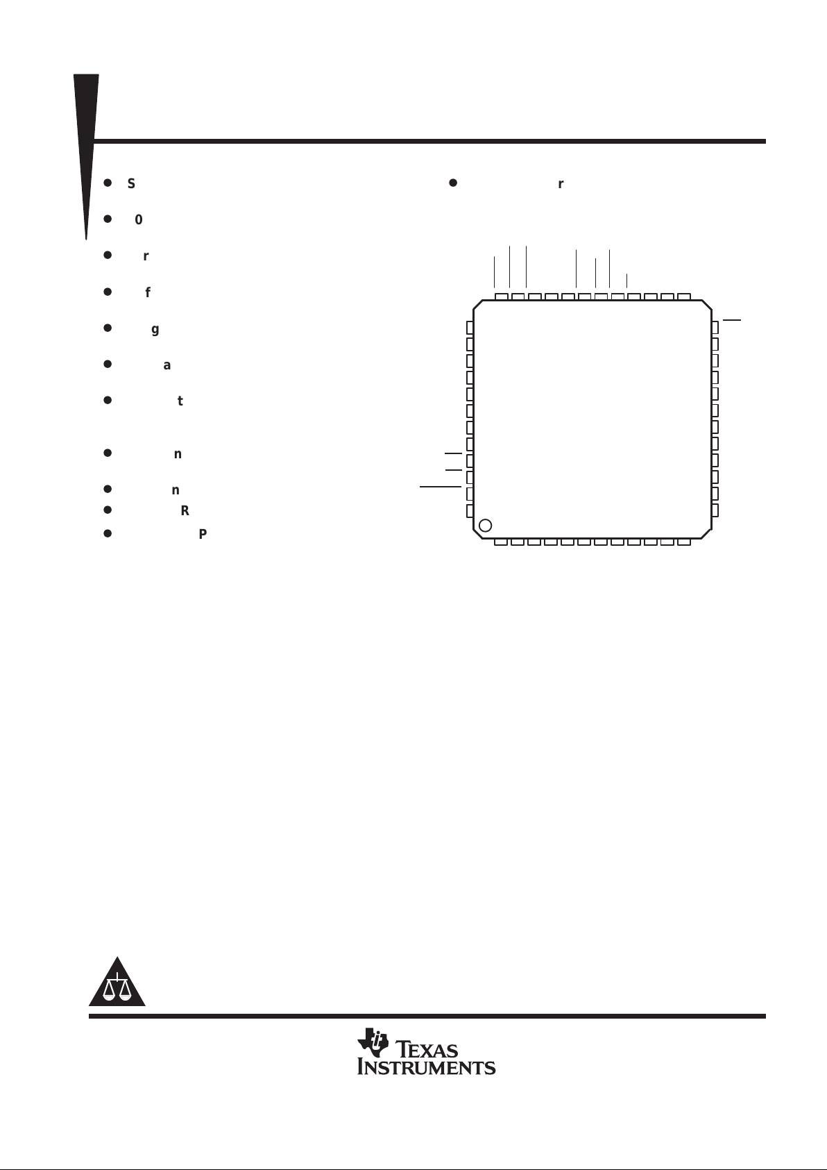
23
OE
SCKP
DACO2
DACO1
AGND3
AV
DD3
DIGND
DIV
DD
D9
D8
D7
D6
24
23
22
21
20
19
18
17
16
15
14
13
4
37
38
39
40
41
42
43
44
45
46
47
48
AGND5
RBD
RMD
RPD
AV
DD5
V
SS
AV
DD1
AGND1
SR
SV
CLCCD
CLREF
5678
RESETCSSDIN
SCLK
35 34 33 32 3136 30
BLKG
CLVDO
ADDOSAVAGND4
D3D4D5
DD2
D0D1D2
28 27 2629
9
10 11 12
25
1
ADCCLK
OBCLP
STBY
VIDEOIN
CCDIN
AGND2
PFB PACKAGE
(TOP VIEW)
AV
DGND
DD
DV
DD4
TLV990PFB
TLV990
3-V, 10-BIT, 28-MSPS AREA CCD AND VIDEO SIGNAL PROCESSOR
SLVS298 – MAY 2000
2
POST OFFICE BOX 655303 • DALLAS, TEXAS 75265
AVAILABLE OPTIONS
PACKAGE DEVICE
T
A
TQFP
(PFB)
–20°C to 75°C TLV990PFB
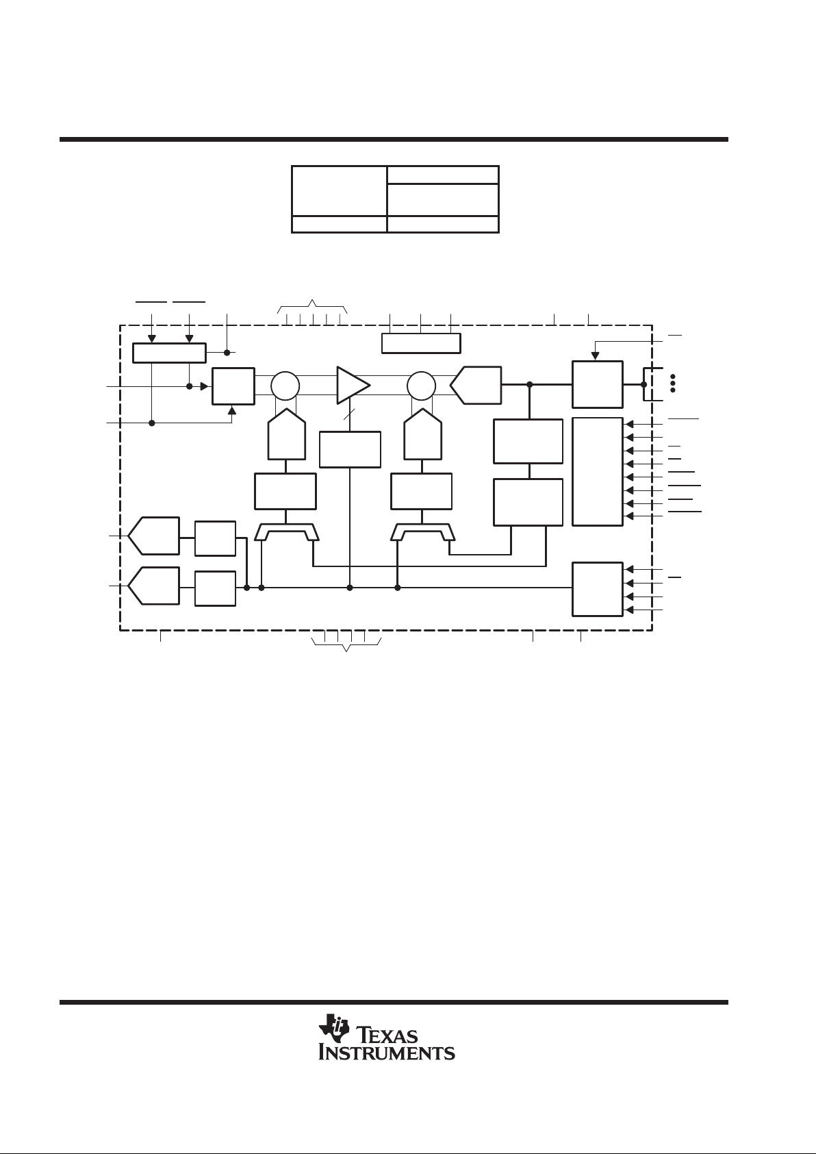
functional block diagram
Σ
10-Bit
ADC
PGA
8-Bit
ADC
Offset
Register
PGA
Regulator
10
Σ
8-Bit
ADC
Offset
Register
INT. REF.
Optical
Black
Pixel Limits
Digital
Averager/
Filter
Three
State
Latch
Timing
and
Control
Logic
Serial
Port
DAC
REG
8-Bit
DAC
DAC
REG
10-Bit
ADC
Clamp
1.2 V REF
CCDIN
VIDEOIN
DACO1
DACO2
CLCCD
CLREF
AVDD1–5
RPD RBD RMD
OE
D0
D9
RESET
CLK
SV
SR
BLKG
OBCLP
STBY
CS
SCLK
SDIN
DIGNDDGND
AGND1–5
VSS
ADDOS
SCKP
CDS/
MUX
DVDDDIV
DD
CLVDO
TLV990
3-V, 10-BIT, 28-MSPS AREA CCD AND VIDEO SIGNAL PROCESSOR
SLVS298 – MAY 2000
3
POST OFFICE BOX 655303 • DALLAS, TEXAS 75265
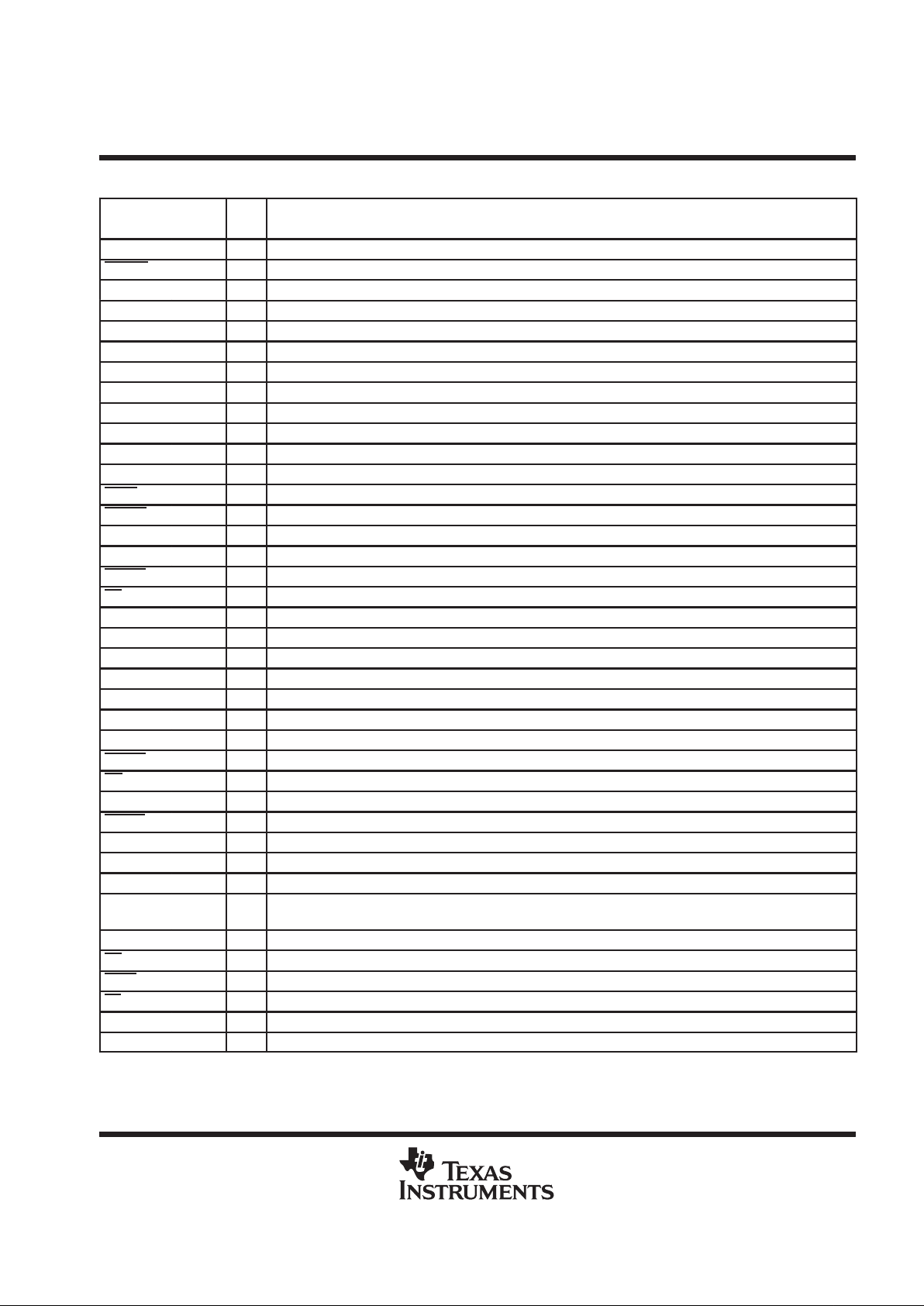
Terminal Functions
TERMINAL I/O DESCRIPTION
NAME NO.
ADCCLK 25 I ADC clock input
ADDOS 34 I A dc offset is added to video input signal when the ADDOS is pulled low.
AGND1 44 Analog ground for internal CDS circuits
AGND2 4 Analog ground for internal PGA circuits
AGND3 20 Analog ground for internal DAC circuits
AGND4 32 Analog ground for internal ADC circuits
AGND5 37 Analog ground for internal REF circuits
AV
DD1
43 Analog supply voltage for internal CDS circuits, 3 V
AV
DD2
3 Analog supply voltage for internal PGA circuits, 3 V
AV
DD3
19 Analog supply voltage for internal DAC circuits, 3 V
AV
DD4
33 Analog supply voltage for internal ADC circuits, 3 V
AV
DD5
41 Analog supply voltage for internal ADC circuits, 3 V
BLKG 36 I Control input. The CDS operation is disabled when the BLKG is pulled low.
CLCCD 47 I CCD signal clamp control input
CCDIN 1 I CCD input
CLREF 48 O Clamp reference voltage output
CLVDO 35 I Video-signal clamp-control input. Only used in manual clamping mode. Active low.
CS 28 I Chip select. A logic low on this input enables the serial port.
D0 – D9 7–16 O 10-bit 3-state ADC output data or offset DACs test data
DACO1 21 O Digital-to-analog converter output1
DACO2 22 O Digital-to-analog converter output2
DGND 5 Digital ground
DIGND 18 Digital interface circuit ground
DIV
DD
17 Digital interface circuit supply voltage, 1.8 V– 4.4 V
DV
DD
6 Digital supply voltage, 3 V
OBCLP 31 I Optical black level and offset calibration control input. Active low.
OE 24 I Output data enable. Active low.
RBD 38 O Internal bandgap reference for external decoupling
RESET 29 I Hardware-reset input, active low. This signal forces a reset of all internal registers
RMD 39 O Ref– output for external decoupling
RPD 40 O Ref+ output for external decoupling
SDIN 27 I Serial data input to configure the internal registers
SCKP 23 I Selects the polarity of SCLK. 0 – active low (high when SCLK is not running), 1 – active high (low when
SCLK is not running)
SCLK 26 I Serial clock input. This clock synchronizes the serial data transfer.
SR 45 I CCD reference level sample clock input
STBY 30 I Hardware power-down control input, active low
SV 46 I CCD signal level sample clock input
VIDEOIN 2 I Analog video signal input
V
SS
42 Silicon substrate, normally connected to analog ground
TLV990
3-V, 10-BIT, 28-MSPS AREA CCD AND VIDEO SIGNAL PROCESSOR
SLVS298 – MAY 2000
4
POST OFFICE BOX 655303 • DALLAS, TEXAS 75265
absolute maximum ratings over operating free-air temperature (unless otherwise noted)
†
Supply voltage, AVDD, DVDD, DIVDD –0.3 V to 6.5 V. . . . . . . . . . . . . . . . . . . . . . . . . . . . . . . . . . . . . . . . . . . . . . . .
Analog input voltage range –0.3 V to AVDD+0.3 V. . . . . . . . . . . . . . . . . . . . . . . . . . . . . . . . . . . . . . . . . . . . . . . . . .
Digital input voltage range –0.3 V to DVDD+0.3 V. . . . . . . . . . . . . . . . . . . . . . . . . . . . . . . . . . . . . . . . . . . . . . . . . .
Operating
virtual junction temperature range, T
J
–40°C to 150°C. . . . . . . . . . . . . . . . . . . . . . . . . . . . . . . . . . . . .
Operating free-air temperature range, TA –20°C to 75°C. . . . . . . . . . . . . . . . . . . . . . . . . . . . . . . . . . . . . . . . . . . .
Storage temperature range, T
stg
–65°C to 150°C. . . . . . . . . . . . . . . . . . . . . . . . . . . . . . . . . . . . . . . . . . . . . . . . . . .
Lead temperature 1,6 mm (1/16 inch) from case for 10 seconds 260°C. . . . . . . . . . . . . . . . . . . . . . . . . . . . . . .
†
Stresses beyond those listed under “absolute maximum ratings” may cause permanent damage to the device. These are stress ratings only, and
functional operation of the device at these or any other conditions beyond those indicated under “recommended operating conditions” is not
implied. Exposure to absolute-maximum-rated conditions for extended periods may affect device reliability.
recommended operating conditions
power supplies
MIN NOM MAX UNIT
Analog supply voltage AV
DD
2.7 3 3.3 V
Digital supply voltage DV
DD
2.7 3 3.3 V
Digital interface supply voltage DIV
DD
1.8 4.4 V
digital inputs, DIVDD = 3 V
MIN NOM MAX UNIT
High-level input voltage, V
IH
0.8DIV
DD
V
Low-level input voltage, V
IL
0.2DIV
DD
V
Input ADCCLK frequency 28 MHz
ADCCLK pulse duration, clock high, t
w(MCLKH)
17.8 ns
ADCCLK pulse duration, clock low, t
w(MCLKL)
17.8 ns
Input SCLK frequency 40 MHz
SCLK pulse duration, clock high, t
w(SCLKH)
12.5 ns
SCLK pulse duration, clock low, t
w(SCLKL)
12.5 ns
TLV990
3-V, 10-BIT, 28-MSPS AREA CCD AND VIDEO SIGNAL PROCESSOR
SLVS298 – MAY 2000
5
POST OFFICE BOX 655303 • DALLAS, TEXAS 75265
electrical characteristics over recommended operating free-air temperature range, TA = 25°C,
AV
DD
=DVDD=3 V, ADCCLK=28 MHz (unless otherwise noted)
total device
PARAMETER TEST CONDITIONS MIN TYP MAX UNIT
AVDD operating current 43 mA
DVDD operating current 7 mA
Device power consumption 150 mW
Power consumption in power-down mode 2 mW
INL Full CCD channel integral nonlinearity
AVDD=DVDD= 2.7 V – 3.3 V,
ADCCLK=18 MSPS, 10 bits
Using best fit method
±0.9 ±2 LSB
DNL Full CCD channel differential nonlinearity
AVDD=DVDD= 2.7 V – 3.3 V,
ADCCLK=18 MSPS, 10 bits
±0.5 ±0.99 LSB
INL Video channel integral nonlinearity
AVDD=DVDD= 2.7 V – 3.3 V,
ADCCLK=28 MSPS, 9 bits
Using best fit method
±0.5 ±2 LSB
DNL Video channel differential nonlinearity
AVDD=DVDD= 2.7 V – 3.3 V,
ADCCLK–28MSPS, 9 bits
±0.4 ±0.99 LSB
No missing code Assured
Full channel output latency 6
CLK
cycles
analog-to-digital converter (ADC)
PARAMETER TEST CONDITIONS MIN TYP MAX UNIT
ADC resolution in CCD mode ADCCLK=18MSPS 10 Bits
Full scale input span 2 V
P-P
Conversion rate 28 MHz
correlated double sample (CDS) and programmable gain amplifier (PGA)
PARAMETER TEST CONDITIONS MIN TYP MAX UNIT
CDS and PGA sample rate 28 MHz
CDS full-scale input span Single-ended input 1 V
Input capacitance of CDS 4 pF
Minimum PGA gain 0 1 dB
Maximum PGA gain 35 36 37 dB
PGA gain resolution 0.045 dB
PGA programming code resolution 10 Bits
internal digital-to-analog converters (DAC) for offset correction
PARAMETER TEST CONDITIONS MIN TYP MAX UNIT
DAC resolution 8 Bits
INL Integral nonlinearity ±0.5 LSB
DNL Differential nonlinearity ±0.5 LSB
Output settling time To 1% accuracy 80 ns
TLV990
3-V, 10-BIT, 28-MSPS AREA CCD AND VIDEO SIGNAL PROCESSOR
SLVS298 – MAY 2000
6
POST OFFICE BOX 655303 • DALLAS, TEXAS 75265
electrical characteristics over recommended operating free-air temperature range, TA = 25°C,
AV
DD
=DVDD=3 V, ADCCLK=28 MHz (unless otherwise noted)
user digital-to-analog converters (DAC)
PARAMETER TEST CONDITIONS MIN TYP MAX UNIT
DAC resolution 8 Bits
INL Integral nonlinearity ±0.75 LSB
DNL Differential nonlinearity ±0.5 LSB
Output voltage range Assured by design 0 V
DD
V
Output settling time 10 pF external load, settle to 1 mV 4 µs
reference voltages
PARAMETER TEST CONDITIONS MIN TYP MAX UNIT
Internal bandgap voltage reference 1.43 1.50 1.58 V
T emperature coef ficient 100 ppm/°C
ADC Ref+
p
2 V
ADC Ref–
Externally decoupled
1 V
digital specifications
PARAMETER TEST CONDITIONS MIN TYP MAX UNIT
Logic inputs
I
IH
High-level input current
–10 10
I
IL
Low-level input current
DIV
DD
= 3
V
–10 10
µ
A
C
i
Input capacitance 5 pF
Logic outputs
V
OH
High-level output voltage IOH = 50 µA, DIVDD = 3 V DIVDD–0.4 V
V
OL
Low-level output voltage IOL = 50 µA, DIVDD = 3 V 0.4 V
I
OZ
High-impedance-state output current ±10 µA
C
o
Output capacitance 5 pF
key timing requirements
PARAMETER TEST CONDITIONS MIN TYP MAX UNIT
t
SRW
SR pulse width
p
10 ns
t
SVW
SV pulse width
Measured at 50% of pulse height
10 ns
t
OD
ADCCLK-to-output data delay 6 ns
t
CSF
CS falling edge to SCLK rising edge 0 ns
t
CSR
SCLK falling edge to CS rising edge 5 ns
TLV990
3-V, 10-BIT, 28-MSPS AREA CCD AND VIDEO SIGNAL PROCESSOR
SLVS298 – MAY 2000
7
POST OFFICE BOX 655303 • DALLAS, TEXAS 75265
0
5
10
15
20
25
30
35
40
0 200 400 600 800 1000 1200
10 BIT-PGA GAIN CURVE
PGA Codes
Gain – dB
Figure 1
TYPICAL CHARACTERISTICS
n
n+1
n
Optical Black Interval
Dummy Black
(Blanking) Interval
Signal Interval
t
SRW
t
SvW
Latency: 6 ADC Cycles
t
OD
CCD
Output
SR
SV
BLKG
CLCCD
OBCLP
ADCCLK
ADC OUT
Figure 2. System Operation Timing Diagram

TLV990
3-V, 10-BIT, 28-MSPS AREA CCD AND VIDEO SIGNAL PROCESSOR
SLVS298 – MAY 2000
8
POST OFFICE BOX 655303 • DALLAS, TEXAS 75265
TYPICAL CHARACTERISTICS
DI14 DI13 DI12 DI8 DI0DI9DI10
1234567 16
DI15
DI14 DI13 DI12 DI8 DI0DI9DI10
1234567 16
DI15
t
CSF
t
CSR
CS
SCLK
SDIN
t
CSF
t
CSR
CS
SCLK
SDIN
SCKP Pin is Pulled Low
SCKP Pin is Pulled High
Figure 3. Serial Interface Timing Diagram

TLV990
3-V, 10-BIT, 28-MSPS AREA CCD AND VIDEO SIGNAL PROCESSOR
SLVS298 – MAY 2000
9
POST OFFICE BOX 655303 • DALLAS, TEXAS 75265
TYPICAL CHARACTERISTICS
CCD IN
SR
SV
ADCCLK
t
SRD
t
SVD
t
ADC_SV
Figure 4. Detailed Internal Timing Diagram
TIMING PARAMETER MIN TYP MAX EXPLANA TION
t
SRD
Delay between sample reset (SR) rising edge and
actual sampling instant (ns)
6 This is the fixed internal delay in the chip. The reset
value of the CCD waveform should be stable until
the end of this period.
t
SVD
Delay between sample video (SV) rising edge and
actual instant of video signal sampling (ns)
6 This is the fixed internal delay in the chip. The video
signal value of the CCD waveform should be stable
until the end of this period.
t
ADC_SV
Time between ADCCLK falling edge and SV rising
edge
10 The timing margin required to ensure the ADCCLK
positive half cycle is in between two SV pulses

TLV990
3-V, 10-BIT, 28-MSPS AREA CCD AND VIDEO SIGNAL PROCESSOR
SLVS298 – MAY 2000
10
POST OFFICE BOX 655303 • DALLAS, TEXAS 75265
APPLICATION INFORMATION
CCDIN
VIDEOIN
AV
DD2
AGND2
DGND
DV
DD
D0
D1
D2
D3
D4
D5
D6D7D8D9DIVDDDIGND
AV
DD3
AGND3
DACO1
DACO2
SCKP
OE
BLKG
CLVDO
ADDOS
AV
DD4
AGND4
OBCLP
STBY
RESET
CS
SDIN
SCLK
SDCCLK
CLREF
CLCCD
SV
SR
AGND1
DD1
AV
SS
V
DD5
AV
RPD
RMD
AGND5
RBD
1
2
3
4
5
6
7
8
9
10
11
12
13 14 15 16 17 18 19 20 21 22 23 24
25
26
27
28
29
30
31
32
33
34
35
36
48 47 46 45 44 43 42 41 40 39 38 37
Inputs
Inputs
Inputs
0.1 µF
AV
DD
1 µF
1 µF
0.1 µF
0.1 µF 1 µF
1 µF
1 µF
Inputs
0.1 µF
AV
DD
0.1 µF
AV
DD
Area
CCD
Video
Signal
0.1 µF
0.1 µF
0.1 µF
AV
DD
0.1 µF
DV
DD
0.1 µF0.1 µF
DIV
DD
AV
DD
Analog GND
Digital GND
AVDD – 3 V
DVDD – 3 V
DIVDD – 1.8 V to 4.4 V
D (0–9)
TLV990PFB
NOTE: All analog outputs should be buffered if the load is resistive, or if the load is capacitive and greater than 2-pF.
Figure 5. Typical Application Connection

TLV990
3-V, 10-BIT, 28-MSPS AREA CCD AND VIDEO SIGNAL PROCESSOR
SLVS298 – MAY 2000
11
POST OFFICE BOX 655303 • DALLAS, TEXAS 75265
REGISTER DEFINITION
serial input data format
DI15 DI14 DI13 DI12 DI11 DI10 DI9 DI8 DI7 DI6 DI5 DI4 DI3 DI2 DI1 DI0
X X A3 A2 A1 A0 D9 D8 D7 D6 D5 D4 D3 D2 D1 D0
A3 A2 A1 A0 D9–D0
0 0 0 0 Control register1 10-bit data be to written into the selected register
0 0 0 1 PGA gain register
0 0 1 0 User DAC1 register
0 0 1 1 User DAC2 register
0 1 0 0 Coarse offset DAC
0 1 0 1 Fine offset DAC
0 1 1 0 Digital Vb register (sets reference code level at the ADC output during the optical black interval)
0 1 1 1 Optical black setup register (sets the number of black pixels per line for digital averaging)
1 0 0 0 Hot pixel limit register (sets the limit for maximum positive deviation of optical black pixel from Vb value)
1 0 0 1 Cold pixel limit register (sets the limit for maximum negative deviation of optical black pixel from Vb value)
1 0 1 0 Control register2 (sets the weight for digital filtering and video modes)
1 0 1 1 Blanking data register (The data in this register appears at digital output during blanking (BLKG is low))
1 1 0 0 ADCCLK internal programmable delay register
1 1 0 1 SR and SV internal programmable delay register
1 1 1 0 Test register
control register1 format
D9 D8 D7 D6 D5 D4 D3 D2 D1 D0
STBY PDD1 PDD2 ACD AFD OBM X SRSV RTOB RTSY
control register1 description
BIT NAME DESCRIPTION
D9 STBY Device power down control: 1 = standby, 0 = active (default)
D8 PDD1 Power down user DAC1: 1 = standby, 0 = active (default)
D7 PDD2 Power down user DAC2: 1 = standby, 0 = active (default)
D6 ACD Coarse-offset DAC mode control:
0 = autocalibration (default), 1 = bypass autocalibration.
Note: When D6 is set to 0, D5 must also be set to 0 (automode). Otherwise, the automode will be disabled on both offset DACs.
D5 AFD Fine offset DAC mode control:
0 = autocalibration (default), 1 = bypass autocalibration.
Note: D5 can be set to 0 with or without D6 being set to 0.
D4 OBM This bit initiates the offset DACs starting sequence.
0 = coarse-offset DAC starts first (default)
1 = fine-offset DAC starts first
D3 X Reserved
D2 SRSV This bit specifies the polarity of SR and SV input pulses.
0 – SR/SV active low (default)
1 – SR/SV active high
D1 RTOB Writing 1 to this bit will reset calculated black-level results in the digital averager.
D0 R TSY Writing 1 to this bit will reset entire system to the default settings (edge sensitive).
TLV990
3-V, 10-BIT, 28-MSPS AREA CCD AND VIDEO SIGNAL PROCESSOR
SLVS298 – MAY 2000
12
POST OFFICE BOX 655303 • DALLAS, TEXAS 75265
REGISTER DEFINITION
PGA register format
D9 D8 D7 D6 D5 D4 D3 D2 D1 D0
Bit 9 Bit 8 Bit 7 Bit 6 Bit 5 Bit 4 Bit 3 Bit 2 Bit 1 Bit 0
Default PGA gain = 0000000000 or 0 dB
user DAC1 and DAC2 registers format
D9 D8 D7 D6 D5 D4 D3 D2 D1 D0
X X Bit 7 Bit 6 Bit 5 Bit 4 Bit 3 Bit 2 Bit 1 Bit 0
Default user DAC register value = XX00000000
coarse offset DAC register format
D9 D8 D7 D6 D5 D4 D3 D2 D1 D0
X SIGN Bit 7 Bit 6 Bit 5 Bit 4 Bit 3 Bit 2 Bit 1 Bit 0
coarse offset DAC register description
BIT NAME DESCRIPTION
D9 X Reserved
D8 SIGN Coarse DAC sign bit, 0 = + sign (default), 1 = – sign
D7–D0 Coarse DAC control data when the D6 in the control register is set at 1.
Default coarse DAC register value = X000000000
fine offset DAC register format
D9 D8 D7 D6 D5 D4 D3 D2 D1 D0
X SIGN Bit 7 Bit 6 Bit 5 Bit 4 Bit 3 Bit 2 Bit 1 Bit 0
fine offset DAC register description
BIT NAME DESCRIPTION
D9 X Reserved
D8 SIGN Fine DAC sign bit, 0 = + sign (default), 1 = – sign
D7–D0 Fine DAC control data when the D5 in the control register is set at 1.
Default fine DAC register value = X000000000
digital Vb (optical black level) register format
D9 D8 D7 D6 D5 D4 D3 D2 D1 D0
Bit 9 Bit 8 Bit 7 Bit 6 Bit 5 Bit 4 Bit 3 Bit 2 Bit 1 Bit 0
Default Vb register value = 40 Hex

TLV990
3-V, 10-BIT, 28-MSPS AREA CCD AND VIDEO SIGNAL PROCESSOR
SLVS298 – MAY 2000
13
POST OFFICE BOX 655303 • DALLAS, TEXAS 75265
REGISTER DEFINITION
optical black setup register format
D9 D8 D7 D6 D5 D4 D3 D2 D1 D0
OMUX1 OMUX0 X X SOFW1 SOFW0 MP PN2 PN1 PN0
optical black setup register description
BIT NAME DESCRIPTION
D8, D9 OMUX1,
OMUX0
These two bits multiplex digital output (data presented at D[9:0] pins):
OMUX1 OMUX0
0 0 D[9:0] = ADC output (default)
0 1 D[9:0] = ADC output
1 0 D[9] = fine/coarse (1/0) autocorrection flag
D[8] = coarse DAC sign
D[7:0] = coarse DAC value
1 1 D[9] = fine/coarse (1/0) autocorrection flag
D[8] = fine DAC sign
D[7:0] = fine DAC value
D7, D6 X Reserved
D5, D4 SOFW1,
SOFW0
These two bits set the digital filter weight when SOF is activated (the SOF bit in control register 2 is set to 1).
SOFW1 SOFW0 Weight
0 0 0 (default)
0 1 1
1 0 2
1 1 3
D3 MP When this bit is 1, the number of optical black pixels to be averaged per line (2N) is multiplied by 3.
By setting the MP and PN2–PN0 bits together, the number of optical black pixels can be programmed to have the following numbers:
1, 2, 3 (1X3), 4, 6 (2×3), 8, 12 (4×3), 16, 24 (8×3), 32, 48 (16×3), 64, 96 (32×3), and 192 (64×3).
Default: MP = 0, no multiplication
D2–D0 PN2–PN0 Number of optical black pixels per line to average = 2
N
N can be 0, 1, 2, 3, 4, 5, and 6. Or number of pixels per line can be 1, 2, 4, 8 (default), 16, 32, or 64.
The maximum number of pixels per line is 64, even if N>6.
Default optical black calibration register value = 0000000011

TLV990
3-V, 10-BIT, 28-MSPS AREA CCD AND VIDEO SIGNAL PROCESSOR
SLVS298 – MAY 2000
14
POST OFFICE BOX 655303 • DALLAS, TEXAS 75265
REGISTER DEFINITION
hot pixel limit register format
D9 D8 D7 D6 D5 D4 D3 D2 D1 D0
Bit 9 Bit 8 Bit 7 Bit 6 Bit 5 Bit 4 Bit 3 Bit 2 Bit 1 Bit 0
Default hot pixel limit register value = 1111111111
cold pixel limit register format
D9 D8 D7 D6 D5 D4 D3 D2 D1 D0
Bit 9 Bit 8 Bit 7 Bit 6 Bit 5 Bit 4 Bit 3 Bit 2 Bit 1 Bit 0
Default cold pixel limit register value = 1111111111
control register2 format
D9 D8 D7 D6 D5 D4 D3 D2 D1 D0
SOF NOS X INM ACL OBOB WT2 WT1 WT0
control register 2 description
BIT NAME DESCRIPTION
D9 SOF 0 – Normal mode (default)
1 – Start of frame (only used when exposure time is changed)
When this bit is set to 1, next positive ADCCLK edge indicates that next pixel line is the beginning of a new frame.
The optical black correction will be performed with one line averaging only (digital filtering weight = 1) and without
hot/cold pixel limits.
D8 Internal test bit (keep at 0)
D7 Jump offset, default = 0
D6 X Reserved
D5 INM This bit selects the input modes.
0 – CCD mode (default)
1 – Video mode
D4 ACL 0 Video mode, autoclamp (default)
1 Video mode, manual clamp
D3 OBOB When this bit is set, the averaged optical black value, instead of the data from the blanking data register, appears at
digital output during blanking.
D2–D0 WT2–WT0 These three bits set the weight for digital filtering.
WT2 WT1 WT0 Weight (effect of the averaged result of each optical black pixel line on overall
optical
black averaging
0 0 0 1 (default)
0011/2
0101/2
0111/8
1 0 0 1/16
1 0 1 1/32
1 1 0 1/64
1 1 1 1/128 (recommended setting)
Default control register2 value = X000000000

TLV990
3-V, 10-BIT, 28-MSPS AREA CCD AND VIDEO SIGNAL PROCESSOR
SLVS298 – MAY 2000
15
POST OFFICE BOX 655303 • DALLAS, TEXAS 75265
REGISTER DEFINITION
blanking data register format
D9 D8 D7 D6 D5 D4 D3 D2 D1 D0
0 0 0 0 BDTA 0 0 0 0 0
blanking data register description
BIT NAME DESCRIPTION
D5 BDTA This register value appears at the digital output when BLKG is low. When this bit is set to 1, digital output during blanking
will be decimal 32. Register default value = 0.
Default = 0000000000
ADCCLK internal delay register format
D9 D8 D7 D6 D5 D4 D3 D2 D1 D0
X X X X X X ADL3 ADL2 ADL1 ADL0
ADCCLK internal delay register description
BIT NAME DESCRIPTION
D9–D4 X Reserved
D3–D0 ADL3–ADL0 These four bits set the internal ADCCLK delay.
ADL3 ADL2 ADL1 ADL0 Typical internal delay
0 0 0 0 0 ns (default)
:
:
1 1 1 1 10 ns
Default register value = XXXXXX0000
SR and SV internal delay register format
D9 D8 D7 D6 D5 D4 D3 D2 D1 D0
X X SVL3 SVL2 SVL1 SVL0 SRL3 SRL2 SRL1 SRL0
SR and SV internal delay register description
BIT NAME DESCRIPTION
D9–D8 X Reserved
D7–D4 SVL3–SVL0 These four bits set the internal SV delay.
SVL3 SVL2 SVL1 SVL0 Typical internal delay
0 0 0 0 0 ns (default)
:
:
1 1 1 1 10 ns
D3–D0 SRL3–SRL0 These four bits set the internal SV delay.
SRL3 SRL2 SRL1 SRL0 Typical internal delay
0 0 0 0 0 ns (default)
:
:
1 1 1 1 10 ns
Default register value = XX00000000

TLV990
3-V, 10-BIT, 28-MSPS AREA CCD AND VIDEO SIGNAL PROCESSOR
SLVS298 – MAY 2000
16
POST OFFICE BOX 655303 • DALLAS, TEXAS 75265
REGISTER DEFINITION
test register format
D9 D8 D7 D6 D5 D4 D3 D2 D1 D0
TB9 TB8 TB7 TB6 X X TB3 TB2 X X
Default test register value = 1000000000
test register description
BIT NAME DESCRIPTION
D9–D6 TB9–TB6 These four bits are used to program internal dc bias current. The bias current programming uses the following
equation:
I
bias
= 8 µA + (code) × 2 µA
Hence, I
bias
varies from 8 µA (code=0000) to 38 µA (code=1111) in linear 2-µA steps.
Default code is 1000.
D5, D4 Reserved
D3 TB3 1 – use external reference, power down internal reference
0 – use internal reference (default)
D2 TB2 This bit selects test input mode:
0 – single-ended input on CCDIN pin,
1 – differential input on both CCDIN and VIDEOIN pins
D1, D0 Reserved

TLV990
3-V, 10-BIT, 28-MSPS AREA CCD AND VIDEO SIGNAL PROCESSOR
SLVS298 – MAY 2000
17
POST OFFICE BOX 655303 • DALLAS, TEXAS 75265
PRINCIPLES OF OPERATION
CCD mode operation
The output from the CCD sensor is first fed to a correlated double sampler (CDS) through the CCDIN pin. The
CCD signal is sampled and held during the reset reference interval and the video signal interval. By subtracting
two resulting voltage levels, the CDS removes low frequency noise from the output of the CCD sensor and
obtains the voltage difference between the CCD reference level and the video level of each pixel. Two
sample/hold control pulses (SR and SV) are required to perform the CDS function.
The CCD output is capacitively coupled to the TL V990. The ac coupling capacitor is clamped to establish proper
dc bias during the dummy pixel interval by the CLCCD input. The bias at the input to the TL V990 is set to 1.2 V.
Normally , CLCCD is applied at sensor’s line rate. A capacitor, with a value ten times larger than that of the input
ac coupling capacitor, should be connected between the CLREF pin and the AGND.
When operating the TL V990 at its maximum speed, the CCD internal source resistance should be smaller than
50 Ω. Otherwise CCD output buffering is required.
The signal is sent to the PGA after the CDS function is complete. The PGA gain can be adjusted from 0 to 36 dB
by programming the internal gain register via the serial port. The PGA is digitally controlled with 10-bit resolution
on a linear dB scale, resulting in a 0.045-dB gain step. The gain can be expressed by the following equation,
Gain = PGA code × 0.045 dB
Where PGA code has a range of 0 to 767.
Due to different exposure times, there might be a sudden optical black level shift at the start of each frame. Thus,
a quick optical black-level correction is desirable. The user can set an internal control bit (the SOF bit in control
register2) to automatically disable the hot/cold pixel limits and to set the digital filtering weighting factor to 1
(equivalent to one-line averaging). In this way the optical black correction could be performed very quickly for
the first line of each frame.
The autocalibration feature can be bypassed if the user prefers to directly program the offset DAC registers.
Switching the autocalibration mode to the direct programming mode requires two register writes. First, the
control bits for the offset DACs in the control register must be changed, then the desired register-offset value
is loaded to the offset DAC registers for proper error correction. If the total offset, including optical black level,
is less than ±255 ADC LSBs, only the FDAC needs to be programmed. When switching from the direct
programming mode to the autocalibration mode, the previous DAC register values are used as starting offsets
rather than default DAC register values.
video mode operation
The TLV990 also provides an analog video-processing channel that consists of an input clamp, a PGA, and an
ADC. Setting the INM bit to 1 in control register2 enables the video channel. The video signal should be
connected to the VIDEOIN pin via a 0.1-µF capacitor, as shown in Figure 5.
The video input has its own clamp circuit operated in two modes: autoclamp, and manual clamp.
In manual clamp mode, the input is clamped when CL VDO pin is pulled low. During this mode, the dc level of
the video sync pulse is forced to the clamp reference voltage (1.2 V).
If the dc level of the video sync pulse is less than the clamp voltage (1.2 V), the autoclamp mode can be selected
(control register2). No external clamp-control signal is required. The CLVDO pin can be left open.
In order to optimize the dynamic range, user can program the fine DAC to position the video signal such that
maximum dynamic range can be achieved. It is also possible to add a dc offset of 255 LSBs to the video signal
by pulling the ADDOS pin low in the video mode. This pin has no effect in the CCD mode.

TLV990
3-V, 10-BIT, 28-MSPS AREA CCD AND VIDEO SIGNAL PROCESSOR
SLVS298 – MAY 2000
18
POST OFFICE BOX 655303 • DALLAS, TEXAS 75265
PRINCIPLES OF OPERATION
ADC
The ADC employs a pipelined architecture to achieve high throughput and low power consumption. Fullydifferential implementation and digital-error correction ensure 10-bit resolution.
The latency of the ADC data output is 6 ADCCLK cycles, as shown in Figure 1. Pulling the OE pin (pin 24) high
puts the ADC output in high impedance.
user DACs
The TLV990 includes two user DACs that can be used for external analog settings. The output voltage of each
DAC can be independently set and has a range of 0 V up to the supply voltage, with an 8-bit resolution. When
the user DACs are not used in a camera system, they can be put in the standby mode by programming control
bits in the control register.
internal timing
The SR and SV signals are required to operate the CDS, as previously explained. The user needs to
synchronize the SR and SV clocks with the CCD signal waveform. The output of the ADC is read out to external
circuitry by the ADCCLK signal, which is also used internally to control both ADC and PGA operations. It is
required that the positive half cycle of the ADCCLK signal always falls in between two adjacent SV pulses as
shown in Fig. 1. The user can then fine tune the ADCCLK timing in relation to the CDS timing to achieve optimal
performance.
The CLCCD signal is used to activate the input clamping and the OBCLP signal is used to activate auto-optical
black and offset correction.
input blanking function
Large input transients may occur at the TL V990’s input during some period of operation which can saturate the
input circuits and cause long recovery time. T o prevent circuit saturation the TL V990 includes an input blanking
function that blocks the input signals by disabling the CDS operation whenever the BLKG input is pulled low.
The TLV990 digital output will be set by the blanking data register after BLKG is pulled low.
NOTE:
If the BLKG pulse is located before the OBCLP pulse, there must be at least 4 pixels between the
rising edge of the BLKG pulse and the falling edge of the OBCLP pulse. If the BLKG pulse is located
after the OBCLP, the minimum number of pixels between the falling edge of the OBCLP and the
falling edge of the BLKG pulse should be equal to the number of optical black pixels per line + 4.
3-wire serial interface
A simple 3-wire (SCLK, SDIN, and CS) serial interface is provided to allow writing to the TLV990 internal
registers. Serial clock SCLK can be run at a maximum frequency of 40 MHz. Serial data SDIN is 16 bits long.
The two leading null bits are followed by four address bits for which the internal register is to be updated, and
then ten bits of data to be written to the register. The CS pin must be held low to enable the serial port. Data
transfer is initiated by the incoming SCLK after CS
falls.
The SCLK polarity is selectable by pulling the SCKP pin either high or low.

TLV990
3-V, 10-BIT, 28-MSPS AREA CCD AND VIDEO SIGNAL PROCESSOR
SLVS298 – MAY 2000
19
POST OFFICE BOX 655303 • DALLAS, TEXAS 75265
PRINCIPLES OF OPERATION
device reset
When pin RESET (pin 29) is pulled low, all internal registers are set to their default values. The device also resets
itself when it is first powered on. In addition, the TLV990 has a software-reset function that resets the device
when writing a control bit to the control register.
See the
register definition
section for the register default values.
voltage references
An internal precision-voltage reference of 1.5 V nominal is provided. This reference voltage is used to generate
the ADC Ref– voltage of 1 V and Ref+ of 2 V. It is also used to set the clamp voltage. All internally-generated
voltages are fixed values and cannot be adjusted.
power-down mode (standby)
The TL V990 implements both hardware and software power-down modes. Pulling pin STBY (pin 30) low puts
the device in the low-power standby mode. Total supply current drops to about 0.6 mA. Setting a power-down
control bit in the control register can also activate the power-down mode. The user can still program all internal
registers during the power-down mode.
power supply
The TL V990 has several power-supply pins. Each major internal analog block has a dedicated AVDD supply pin.
All internal digital circuitry is powered by DVDD. Both A VDD and DVDD are 3-V nominal.
The DIVDD and DIGND pins supply power to the output digital driver (D9–D0). The DIVDD is independent of the
DVDD and can be operated from 1.8 V to 4.4 V . This allows the outputs to interface with digital ASICs requiring
different supply voltages.
ground and decoupling
All ground pins of the TL V990 are not internally connected and must be connected externally to PCB ground.
General practices should apply to the PCB design to limit high-frequency transients and noise that are fed back
into the supply and reference lines. This requires that the supply and reference pins be sufficiently bypassed.
In the case of power supply decoupling, 0.1-µF ceramic chip capacitors are adequate to keep the impedance
low over a wide frequency range. Recommended external decoupling for the three voltage-reference pins is
shown in Figure 4. Since their effectiveness depends largely on the proximity to the individual supply pin, all
decoupling capacitors should be placed as close as possible to the supply pins.
To reduce high-frequency and noise coupling, it is highly recommended that digital and analog grounds be
shorted immediately outside the package. This can be accomplished by running a low-impedance line between
DGND and AGND under the package.

TLV990
3-V, 10-BIT, 28-MSPS AREA CCD AND VIDEO SIGNAL PROCESSOR
SLVS298 – MAY 2000
20
POST OFFICE BOX 655303 • DALLAS, TEXAS 75265
PRINCIPLES OF OPERATION
automatic optical black and offset correction
In the TL V990, the optical black and system channel-offset corrections are performed by an autodigital feedback
loop. Two DACs are used to compensate for both channel of fset and optical black offset. A coarse correction
DAC (CDAC) is located before PGA gain stage, and a fine correction DAC (FDAC) is located after the gain stage.
The digital-calibration system is capable of correcting the optical black and channel offset down to one ADC LSB
accuracy .
The TLV990 automatically starts autocalibration whenever the OBCLP input is pulled low. The OBCLP pulse
should be wide enough to cover one positive half cycle of the ADCCLK, as shown in Figure 1.
For each line, the optical black pixels plus the channel offset are sampled and converted to digital data by the
ADC. A digital circuit averages the data during the optical black pixels. The averaged result is compared digitally
with the desired output code stored in the Vb register (default is 40H), then the FDAC is adjusted by control logic
to make the ADC output equal to the Vb. If the offset is out of the range of the FDAC (±255 ADC LSBs), the error
is corrected by both the CDAC and the FDAC. The CDAC increments or decrements by one CDAC LSB,
depending on whether the offset is negative of positive, until the output is within the range of the FDAC. The
remaining residue is corrected by the FDAC.
The relationship among the FDAC, CDAC, and ADC in terms of number of ADC LSBs is as follows:
1 FDAC LSB = 1 ADC LSB,
1 CDAC LSB = PGA linear gain × n ADC LSB.
Where n is:
4 for 0 =< gain code <64
3 for 64 =< gain code <96
2 for 96 =< gain code <128
1 for 128 =< gain code
For example, if PGA gain = 2 (6 dB), then, 1 CDAC LSB = 2 x 4 ADC LSBs = 8 ADC LSBs.
After autocalibration is complete, the ADC’s digital output during CCD signal interval can be expressed by the
following equation:
ADC output [D9–D0] = CCD_input × PGA gain + Vb,
Where Vb is the desired black level selected by user. The total of fset, including optical black offset, is calibrated
to be equal to the Vb by adjusting the offset correction DACs during autocalibration.
A weighted rolling average of the optical black pixels is taken during averaging. The weighting factor can be
programmed in control register2. The weighting factor determines the speed of convergence of the digital
filtering implemented within the CCD signal processor. Weighting factors closer to 1 result in faster
convergence. As the weighting factor decreases towards its minimum value of 1/128, the speed of convergence
of the digital filtering decreases.
The algorithm also takes
hot pixels
and
cold pixels
into consideration. A hot optical black pixel is a defective
pixel that generates too much charge, while a cold pixel is the one that generates very little or no charge. A digital
comparator compares the digitized optical black pixels with user-selected hot and cold pixel limits. If the optical
black pixel value is out of range, then that
hot or cold pixel
is replaced with the value of the previous pixel.

TLV990
3-V, 10-BIT, 28-MSPS AREA CCD AND VIDEO SIGNAL PROCESSOR
SLVS298 – MAY 2000
21
POST OFFICE BOX 655303 • DALLAS, TEXAS 75265
PRINCIPLES OF OPERATION
automatic optical black and offset correction (continued)
Due to different exposure times, there might be a sudden optical black level shift at the start of each frame. Thus,
a quick optical black level correction is desirable. The user can set an internal control bit (the SOF bit in control
register2) to automatically disable the hot/cold pixel limits and to set the digital filtering weighting factor to 1
(equivalent to one-line averaging). In this way the optical black correction could be performed very quickly for
the first line of each frame.
The number of black pixels in each line is programmable. The number of black pixels per line that can be
averaged is 2N, where N can be any integer from 0 to 6.
The autocalibration feature can be bypassed if the user prefers to directly program the offset DAC registers.
Switching the autocalibration mode to the direct-programming mode requires two register writes. First, the
control bits for the offset DACs in the control register must be changed, then the desired offset value for the
register is loaded to the offset DAC registers for proper error correction. If the total offset, including optical black
level is less than ±255 ADC LSBs, only the FDAC needs to be programmed. When switching from direct-
programming mode to autocalibration mode, the previous DAC register values, rather than default DAC register
values, are used as starting offsets.

IMPORTANT NOTICE
T exas Instruments and its subsidiaries (TI) reserve the right to make changes to their products or to discontinue
any product or service without notice, and advise customers to obtain the latest version of relevant information
to verify, before placing orders, that information being relied on is current and complete. All products are sold
subject to the terms and conditions of sale supplied at the time of order acknowledgment, including those
pertaining to warranty, patent infringement, and limitation of liability.
TI warrants performance of its semiconductor products to the specifications applicable at the time of sale in
accordance with TI’s standard warranty. Testing and other quality control techniques are utilized to the extent
TI deems necessary to support this warranty. Specific testing of all parameters of each device is not necessarily
performed, except those mandated by government requirements.
Customers are responsible for their applications using TI components.
In order to minimize risks associated with the customer’s applications, adequate design and operating
safeguards must be provided by the customer to minimize inherent or procedural hazards.
TI assumes no liability for applications assistance or customer product design. TI does not warrant or represent
that any license, either express or implied, is granted under any patent right, copyright, mask work right, or other
intellectual property right of TI covering or relating to any combination, machine, or process in which such
semiconductor products or services might be or are used. TI’s publication of information regarding any third
party’s products or services does not constitute TI’s approval, warranty or endorsement thereof.
Copyright 2000, Texas Instruments Incorporated
 Loading...