

TLV840CADL29
VDD
GND
RESET
Microcontroller
VDD
5 V
RESET
LDO
3.3 V
CT
IN
OUT
*R
pu
*R
pu
only for open-drain output
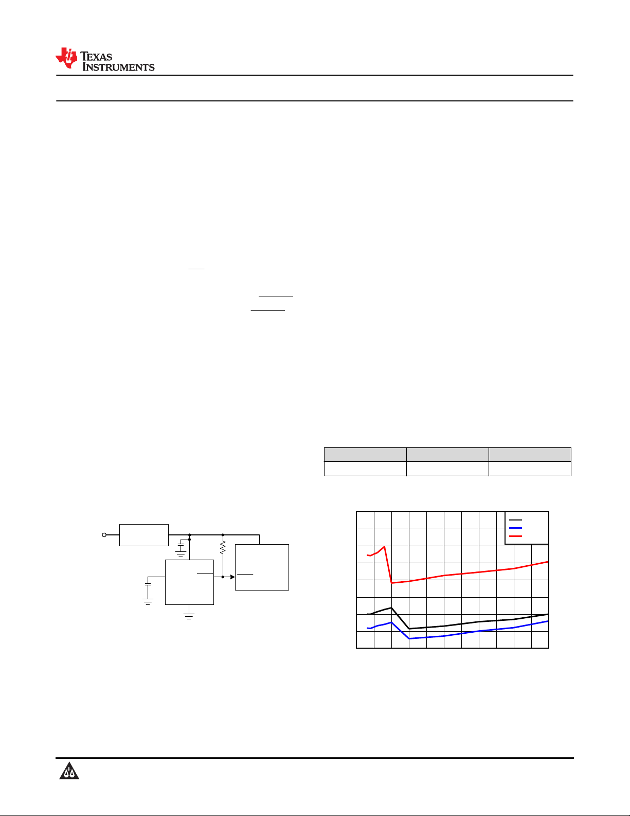
VDD (V)
I
DD
(µA)
0.5 1 1.5 2 2.5 3 3.5 4 4.5 5 5.5 6
0.08
0.12
0.16
0.2
0.24
0.28
0.32
0.36
0.4
IDDv
25°C
-40°C
125°C
TLV840
www.ti.com
SNVSBC3C – DECEMBER 2019 – REVISED SEPTEMBER 2020
SNVSBC3C – DECEMBER 2019 – REVISED SEPTEMBER 2020
TLV840
TLV840 Nano-Power Ultra-Low Voltage Supervisor with Adjustable Reset Time Delay
1 Features
• Operating voltage range : 0.7 V to 6 V
• Nano supply current : 120 nA (Typical)
• Fixed threshold voltage (V
): 0.8 V to 5.4 V
IT-
– Threshold voltages available in 100mV steps
– High accuracy: ±0.5% (Typical)
– Built-in hysteresis (V
): 5% (Typical)
HYS
• Reset time delay (tD): capacitor-based
programmable (TLV840C, TLV840M)
– Minimum time delay: 40 µs (typical) without
capacitor
• Active-low manual reset (MR) (TLV840M)
• Four output topologies:
– TLV840xxDL: open-drain, active-low (RESET)
– TLV840xxPL: push-pull, active-low (RESET)
– TLV840xxDH: open-drain, active-high (RESET)
– TLV840xxPH: push-pull, active-high (RESET)
• Wide temperature range: –40°C to +125°C
• Package: SOT23-5 (DBV)
2 Applications
• Motor Drives
• Factory Automation and Control
• Home Theater and Entertainment
• Electronic Point of Sale
• Grid Infrastructure
• Data Center and Enterprise Computing
• Multifunction Printer
3 Description
The TLV840 family of voltage supervisors or reset ICs
can operate at high voltage levels while maintaining
very low quiescent current across the whole VDD and
temperature range. TLV840 offers best combination of
low power consumption, high accuracy and low
propagation delay (t
Reset output signal is asserted when the voltage at
VDD drops below the negative voltage threshold
(V
). Reset signal is cleared when VDD rise above
IT-
V
plus hysteresis (V
IT-
(tD) expires. Reset time delay can be programmed by
connecting a capacitor between the CT pin and
ground for TLV840C and TLV840M. For a minimum
reset delay time the CT pin can be left floating.
TLV840N does not offer a programmable delay and
offers fixed reset delay timing options: 40 µs, 2 ms, 10
ms, 30 ms, 50 ms, 80 ms, 100 ms, 150 ms, 200 ms.
Additional features: Low power-on reset voltage
(V
), built-in glitch immunity protection for VDD,
POR
built-in hysteresis, low open-drain output leakage
current (I
). TLV840 is a perfect voltage
lkg(OD)
monitoring solution for industrial applications and
battery-powered / low-power applications.
Device Information
PART NUMBER PACKAGE
TLV840 SOT-23 (5) (DBV) 2.90 mm × 1.60 mm
(1) For package details, see the mechanical drawing addendum
at the end of the data sheet.
= 30 µs typical).
p_HL
) and the reset time delay
HYS
(1)
BODY SIZE (NOM)
Typical Application Circuit
Copyright © 2020 Texas Instruments Incorporated
An IMPORTANT NOTICE at the end of this data sheet addresses availability, warranty, changes, use in safety-critical applications,
intellectual property matters and other important disclaimers. PRODUCTION DATA.
Product Folder Links: TLV840
Typical Supply Current
Submit Document Feedback
1

TLV840
SNVSBC3C – DECEMBER 2019 – REVISED SEPTEMBER 2020
www.ti.com
Table of Contents
1 Features............................................................................1
2 Applications..................................................................... 1
3 Description.......................................................................1
4 Revision History.............................................................. 2
5 Device Comparison......................................................... 3
6 Pin Configuration and Functions...................................4
Pin Functions.................................................................... 4
7 Specifications.................................................................. 5
7.1 Absolute Maximum Ratings ....................................... 5
7.2 ESD Ratings .............................................................. 5
7.3 Recommended Operating Conditions ........................5
7.4 Thermal Information ...................................................5
7.5 Electrical Characteristics ............................................6
7.6 Timing Requirements .................................................7
7.7 Timing Diagrams ........................................................8
7.8 Typical Characteristics................................................9
8 Detailed Description......................................................10
8.1 Overview................................................................... 10
8.2 Functional Block Diagram......................................... 10
8.3 Feature Description...................................................10
8.4 Device Functional Modes..........................................14
9 Application and Implementation.................................. 15
9.1 Application Information............................................. 15
9.2 Typical Application.................................................... 15
10 Power Supply Recommendations..............................18
11 Layout...........................................................................19
11.1 Layout Guidelines................................................... 19
11.2 Layout Example...................................................... 19
12 Device and Documentation Support..........................20
12.1 Device Nomenclature..............................................20
12.2 Receiving Notification of Documentation Updates..21
12.3 Support Resources................................................. 21
12.4 Trademarks.............................................................21
13 Mechanical, Packaging, and Orderable
Information.................................................................... 21
4 Revision History
NOTE: Page numbers for previous revisions may differ from page numbers in the current version.
Changes from Revision B (July 2020) to Revision C (September 2020) Page
• Updated the numbering format for tables, figures, and cross-references throughout the document..................1
• Updated Pin Connections................................................................................................................................... 4
• Added Timing Diagram....................................................................................................................................... 8
• New Typical Characteristics................................................................................................................................9
Changes from Revision A (February 2020) to Revision B (July 2020) Page
• APL to RTM release............................................................................................................................................1
Changes from Revision * (December 2019) to Revision A (February 2020) Page
• Initial APL Release............................................................................................................................................. 1
2 Submit Document Feedback
Product Folder Links: TLV840
Copyright © 2020 Texas Instruments Incorporated
TLV 840 X X XX XX XXX
Feature Option
N: no capacitor delay (CT),
no manual reset (MR)
C: Capacitor delay (CT)
M: Capacitor delay (CT) and
manual reset (MR)
Output Type
DL: Open-drain,
active-low
PL: Push-pull,
active-low
DH: Open-drain,
active-high
PH: Push-pull,
active-high
Detect Voltage Threshold
08: 0.8V
...
54: 5.4V
Delay Optio n
A: 40 µs
B: 2 ms
C: 10 ms
D: 30 ms
E: 50 ms
F: 80 ms
G: 100 ms
H: 150 ms
I: 200 ms
Package
DBV: SOT23
www.ti.com
SNVSBC3C – DECEMBER 2019 – REVISED SEPTEMBER 2020
5 Device Comparison
Figure 5-1 shows the device naming nomenclature to compare the different device variants. See Table 12-1 for a
more detailed explanation.
Figure 5-1. Device Naming Nomenclature
TLV840
Orderable part numbers starting with TLV840C and TLV840M are only available with the delay option A.
However, longer delays can be achieved through an external capacitor on the CT pin. Leaving the CT pin
floating will result in typical 40us delay for these 2 feature options.
Copyright © 2020 Texas Instruments Incorporated
Product Folder Links: TLV840
Submit Document Feedback
3
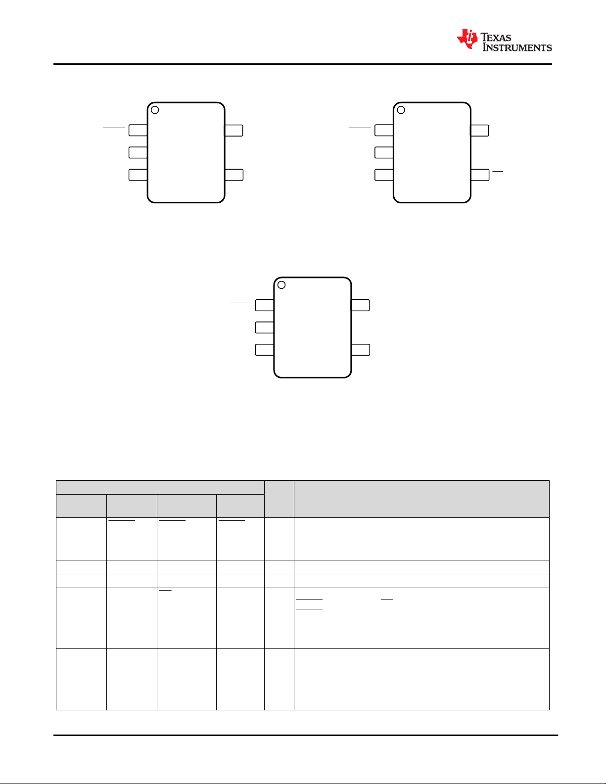
1RESET
2VDD
3GND 4
5
CT
Not to scale
NC
1RESET
2VDD
3GND 4
5
CT
Not to scale
MR
1RESET
2VDD
3GND 4
5 NC
Not to scale
NC
TLV840
SNVSBC3C – DECEMBER 2019 – REVISED SEPTEMBER 2020
6 Pin Configuration and Functions
www.ti.com
Figure 6-1. Pin Configuration TLV840C,
DBV Package, 5-Pin SOT-23,
TLV840C Top View
Figure 6-2. Pin Configuration TLV840M,
DBV Package, 5-Pin SOT-23,
TLV840M Top View
Figure 6-3. Pin Configuration TLV840N,
DBV Package, 5-Pin SOT-23,
TLV840N Top View
Pin Functions
PIN
PIN
TLV840CxL TLV840MxL TLV840NxL
NUMBER
1 RESET RESET RESET O Active-Low Output Reset Signal: This pin is driven logic low when
2 VDD VDD VDD I Input Supply Voltage TLV840 monitors VDD voltage
3 GND GND GND _ Ground
4 NC MR NC I Manual Reset Pull this pin to a logic low to assert a reset signal in the
5 CT CT NC - Capacitor Time Delay Pin. The CT pin offers a user-programmable
I/O DESCRIPTION
VDD voltage falls below the negative voltage threshold (V
remains low (asserted) for the delay time period (tD) after VDD voltage
rises above V
IT+=VIT-+VHYS
.
RESET output pin. After MR pin is left floating or pulls to logic high, the
RESET output deasserts to the nominal state after the reset delay time
(tD)expires.
NC stands for “No Connect”. The pin can be left floating.
Recommended connection to GND.
delay time. Connect an external capacitor on this pin to adjust time
delay. When not in use leave pin floating for the smallest fixed time
delay.
NC stands for “No Connect”. The pin can be left floating.
Recommended connection to GND.
). RESET
IT-
4 Submit Document Feedback
Copyright © 2020 Texas Instruments Incorporated
Product Folder Links: TLV840
www.ti.com
SNVSBC3C – DECEMBER 2019 – REVISED SEPTEMBER 2020
7 Specifications
TLV840
7.1 Absolute Maximum Ratings
over operating free-air temperature range, unless otherwise noted
Voltage VDD –0.3 6.5 V
Voltage
CT, MR
RESET (TLV840xxDL) –0.3 6.5
Current RESET, RESET pin –20 20 mA
Temperature
Temperature
(4)
(4)
Operating ambient temperature, T
Storage, T
(1) Stresses beyond those listed under Absolute Maximum Rating may cause permanent damage to the device. These are stress ratings
only, which do not imply functional operation of the device at these or any other conditions beyond those indicated under
Recommended Operating Condition. Exposure to absolute-maximum-rated conditions for extended periods may affect device
reliability.
(2) If the logic signal driving
MR is less than VDD, then additional current flows into VDD and out of MR.
(3) The absolute maximum rating is (VDD + 0.3) V or 6.5 V, whichever is smaller
(4) As a result of the low dissipated power in this device, it is assumed that TJ = TA.
(2)
, RESET (TLV840xxPL) –0.3 VDD+0.3
A
stg
7.2 ESD Ratings
Human body model (HBM), per ANSI/ESDA/JEDEC
(1)
V
(ESD)
Electrostatic discharge
JS-001
Charged device model (CDM), per JEDEC specification
JESD22-C101
(2)
(1)
MIN MAX UNIT
(3)
V
–40 125
–65 150
℃
VALUE UNIT
± 2000
V
± 750
(1) JEDEC document JEP155 states that 500-V HBM allows safe manufacturing with a standard ESD control process.
(2) JEDEC document JEP157 states that 250-V CDM allows safe manufacturing with a standard ESD control process.
7.3 Recommended Operating Conditions
over operating free-air temperature range (unless otherwise noted)
MIN NOM MAX UNIT
Voltage
Current RESET pin current –5 5 mA
T
A
VDD (TLV840xxxL) 0.7 6
CT, RESET (TLV840xxxL), MR 0 6
Operating ambient temperature –40 125 ℃
V
7.4 Thermal Information
TLV840
THERMAL METRIC
R
θJA
R
θJC(top)
R
θJB
ψ
JT
ψ
JB
R
θJC(bot)
Junction-to-ambient thermal resistance 193.5 °C/W
Junction-to-case (top) thermal resistance 117.9 °C/W
Junction-to-board thermal resistance 98.5 °C/W
Junction-to-top characterization parameter 43.4 °C/W
Junction-to-board characterization parameter 97.8 °C/W
Junction-to-case (bottom) thermal resistance N/A °C/W
(1) For more information about traditional and new thermal metrics, see the Semiconductor and IC Package Thermal Metrics application
report.
(1)
UNITDBV (SOT23-5)
5 PINS
Copyright © 2020 Texas Instruments Incorporated
Product Folder Links: TLV840
Submit Document Feedback
5
TLV840
SNVSBC3C – DECEMBER 2019 – REVISED SEPTEMBER 2020
7.5 Electrical Characteristics
At 0.7 V ≤ VDD ≤ 6 V, CT = MR = Open, RESET pull-up resistor (R
load (C
VDD ramp rate ≤ 100 mV/µs. Typical values are at TA = 25℃
COMMON PARAMETERS
V
DD
V
IT–
V
HYS
I
DD
V
MR_L
V
MR_H
R
MR
R
CT
TLV840xxDL (Open-drain active-low)
V
POR
V
OL
I
lkg(OD)
TLV840xxPL (Push-pull active-low)
V
POR
V
OL
V
OH
) = 10 pF and over operating free-air temperature range –40℃ to 125℃, unless otherwise noted.
LOAD
PARAMETER TEST CONDITIONS MIN TYP MAX UNIT
Input supply voltage TLV840xxxL 0.7 6 V
V
= 0.8 V to 1.7 V –2.5 ±0.5 2.5
Negative-going input threshold accuracy
(1)
Hysteresis on V
pin 2.5 5 7 %
IT–
IT-
V
= 1.8 V to 5.4 V –2 ±0.5 2
IT-
VDD = 2 V
V
= 0.8 V to 1.8 V
IT–
Supply current into VDD pin
(2)
VDD = 6 V
V
= 0.8 V to 5.5 V
IT–
Manual reset logic low input
Manual reset logic high input
(2)
(2)
Manual reset internal pull-up resistance 100 kΩ
CT pin internal resistance 500 kΩ
V
= 300 mV
Power on Reset Voltage
(3)
Low level output voltage
Open-Drain output leakage current
Power on Reset Voltage
(3)
Low level output voltage
High level output voltage
OL(max)
I
OUT(Sink)
= 15 µA
VDD = 0.7 V, 0.8 V ≤ V
I
OUT(Sink)
= 15 µA
VDD =1.5 V, 1.6 V ≤ V
I
OUT(Sink)
= 500 µA
VDD = 3.3 V, 3.4 V ≤ V
I
VDD = V
OUT(Sink)
= 2 mA
PULLUP
= 6V
TA = –40℃ to 85℃
VDD = V
V
OL(max)
I
OUT(Sink)
= 6V 10 350 nA
PULLUP
= 300 mV
= 15 µA
VDD = 0.7 V, 0.8 V ≤ V
I
OUT(Sink)
= 15 µA
VDD = 1.5 V, 1.6 V ≤ V
I
OUT(Sink)
= 500 µA
VDD = 3.3 V, 3.4 V ≤ V
I
V
I
V
I
V
I
= 2 mA
OUT(Sink)
= 1.8 V, 0.8 V ≤ V
DD
OUT(Source)
DD
OUT(Source)
DD
OUT(Source)
= 500 µA
= 3.3 V, 1.5 V ≤ V
= 500 µA
= 6 V, 3.1 V ≤ V
= 2 mA
IT–
IT–
IT–
IT–
IT–
IT–
IT–
IT–
≤ 5.5 V
IT–
) = 100 kΩ to VDD, output reset
pull-up
TA = –40℃ to
85℃
TA = –40℃ to
85℃
≤ 1.5 V
≤ 3.3 V
≤ 5.5 V
≤ 1.5 V
≤ 3.3 V
≤ 5.5 V
≤ 1.4 V
≤ 3.0 V
0.7V
0.8V
0.8V
0.8V
DD
DD
DD
DD
www.ti.com
0.12 0.3
0.12 1.0
0.15 0.4
0.15 1.2
0.3V
DD
700 mV
300
300
300
10 100 nA
700 mV
300
300
300
%
µA
V
V
mV
mV
V
(1) V
threshold voltage range from 0.8 V to 5.4 V (for DL, PL versions) in 100 mV steps
IT–
(2) If the logic signal driving MR is less than VDD, then I
(3) V
is the minimum VDD voltage level for a controlled output state
POR
6 Submit Document Feedback
current increases based on voltage differential
DD
Product Folder Links: TLV840
Copyright © 2020 Texas Instruments Incorporated
www.ti.com
7.6 Timing Requirements
At 0.7 V ≤ VDD ≤ 6 V, CT = MR = Open, RESET pull-up resistor (R
load (C
VDD ramp rate ≤ 100 mV/µs. Typical values are at TA = 25℃
t
P_HL
t
D
t
GI_VIT–
t
MR_PW
t
MR_RES
t
MR_tD
) = 10 pF and over operating free-air temperature range –40℃ to 125℃, unless otherwise noted.
LOAD
PARAMETER TEST CONDITIONS MIN TYP MAX UNIT
Propagation detect delay for VDD falling
below V
IT–
TLV840xA
Reset time delay
TLV840CA,
TLV840MA
Glitch immunity V
MR pin pulse duration to assert reset
IT–
(3)
Propagation delay from MR low to reset
assertion
Delay from MR release to reset deassert
V
: (V
DD
(1)
+ 10%) to (V
IT+
CT pin = Open or NC
(V
- 10%) to (V
IT-
IT+
CT pin = 10 nF 6.2 ms
CT pin = 1 µF 619 ms
5% V
overdrive
IT–
(2)
VDD = 3.3 V,
MR = V
MR_H
to V
MR_L
VDD = 3.3 V,
MR = V
MR_L
to V
MR_H
SNVSBC3C – DECEMBER 2019 – REVISED SEPTEMBER 2020
) = 100 kΩ to VDD, output reset
pull-up
– 10%)
IT–
+ 10%)
30 50 µs
40 80 µs
10 µs
500 ns
1 µs
t
D
TLV840
ms
(1) t
(2) Overdrive % = [(VDD/ V
measured from threshold trip point (V
P_HL
) – 1] × 100%
IT–
) to RESET assert. V
IT–
(3) Refer section on Manual Reset Input for min pulse width needed on
= V
IT+
MR pin
IT–
+ V
HYS
Copyright © 2020 Texas Instruments Incorporated
Product Folder Links: TLV840
Submit Document Feedback
7
t
D
t
P_HL
VDD
V
POR
V
OH
V
OL
V
IT+
V
IT-
RESET
t
P_HL
V
DD(0v)
tD
t
D
t
D
t
P_HL
VDD
V
POR
V
OH
V
OL
V
IT+
V
IT-
RESET
t
P_HL
t
D
t
D
TLV840
SNVSBC3C – DECEMBER 2019 – REVISED SEPTEMBER 2020
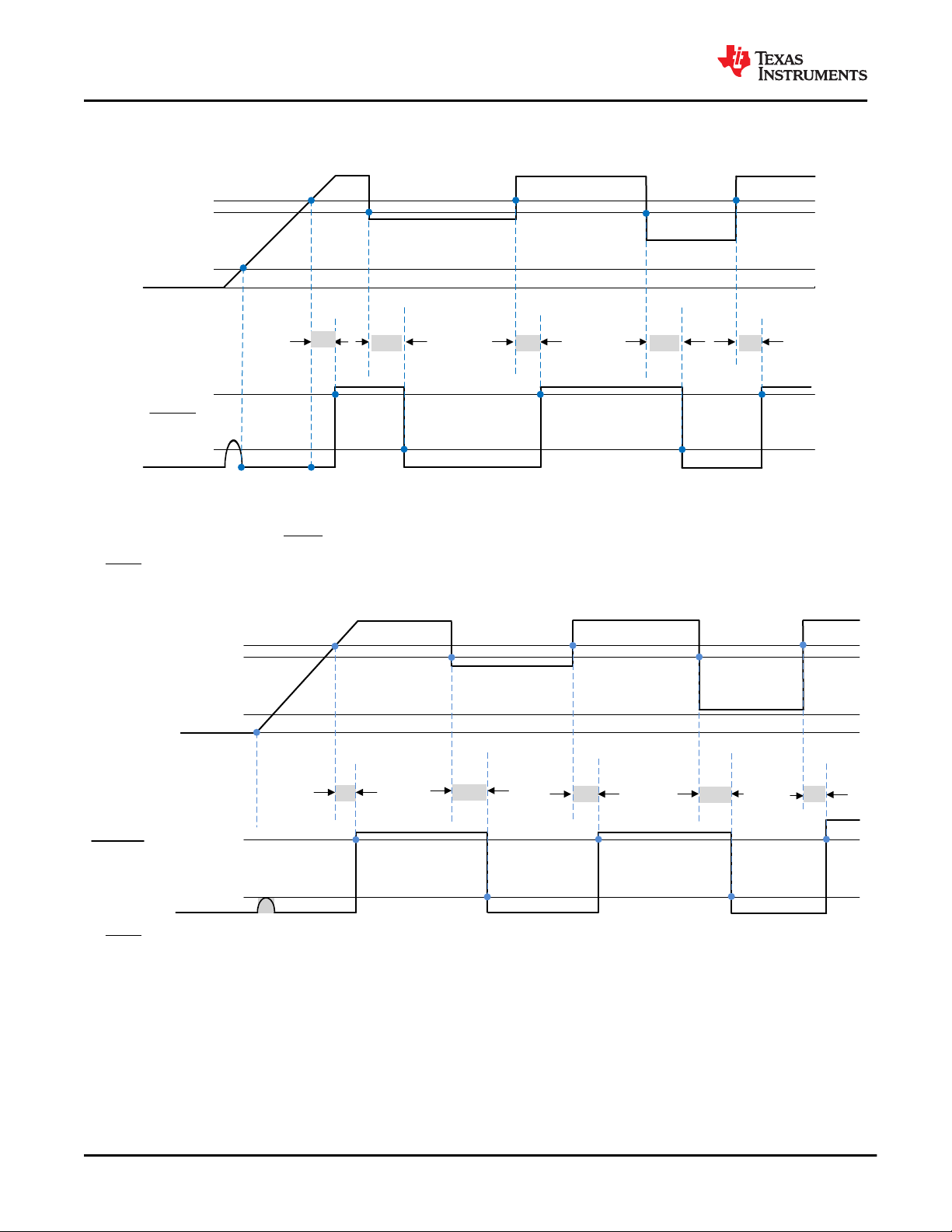
7.7 Timing Diagrams
www.ti.com
(1) Open-Drain timing diagram where RESET is pulled up to VDD via a pull-up resistor
(2) RESET output is undefined when VDD is < V
POR
Figure 7-1. Timing Diagram TLV840DL (Open-Drain Active-Low)
(3) RESET output is undefined when VDD is < V
Figure 7-2. Timing Diagram TLV840PL (Push-Pull Active-Low)
and limited to VOL for VDD slew rate = 100mV / μS
POR
8 Submit Document Feedback
Copyright © 2020 Texas Instruments Incorporated
Product Folder Links: TLV840
VDD (V)
I
DD
(µA)
0.5 1 1.5 2 2.5 3 3.5 4 4.5 5 5.5 6
0.08
0.12
0.16
0.2
0.24
0.28
0.32
0.36
0.4
IDDv
25°C
-40°C
125°C
www.ti.com
SNVSBC3C – DECEMBER 2019 – REVISED SEPTEMBER 2020
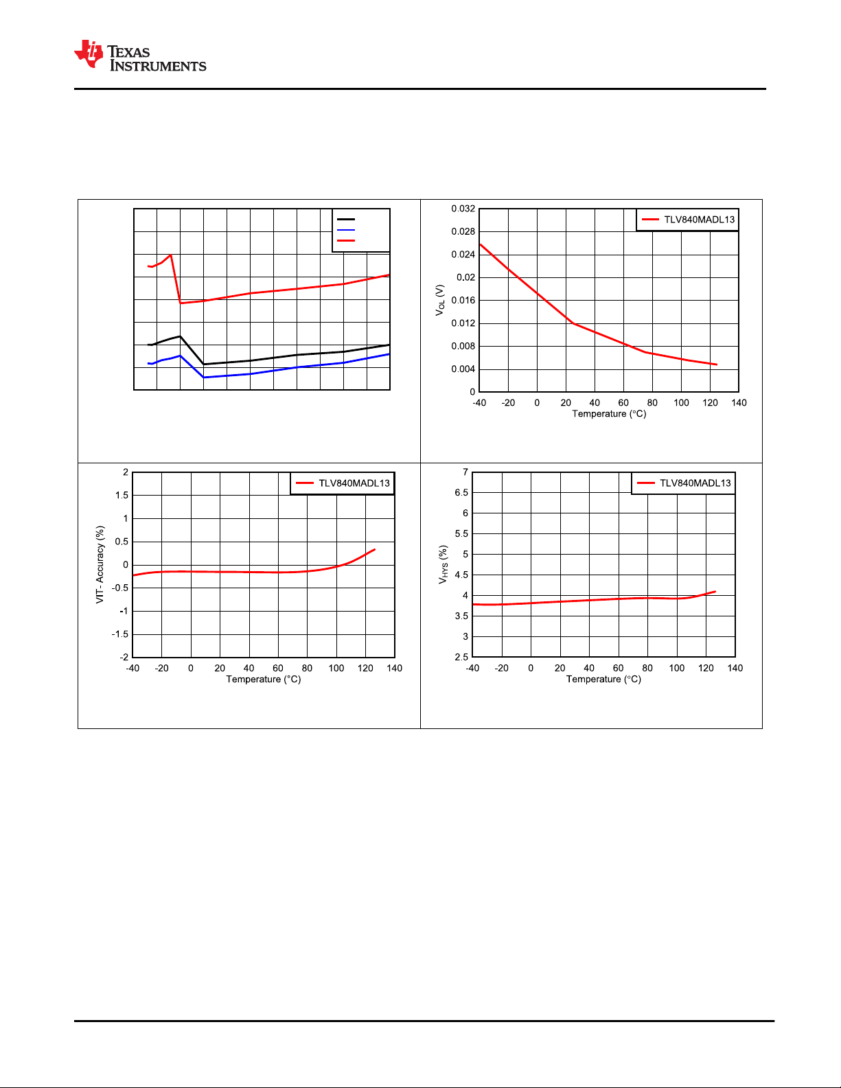
7.8 Typical Characteristics
Typical characteristics show the typical performance of the TLV840 device. Test conditions are TA = 25°C,
TLV840
VDD = 3.3 V, R
Pull-Up
= 100 kΩ, C
= 50 pF, unless otherwise noted.
LOAD
Figure 7-3. Supply Current vs Supply Voltage for
TLV840MADL13
Figure 7-4. Low Output Voltage (VOL) vs
Temperature for TLV840MADL13 (VDD = 0.7 V)
Figure 7-5. Voltage Threshold Accuracy vs
Temperature for TLV840MADL13
Copyright © 2020 Texas Instruments Incorporated
Figure 7-6. Voltage Hysteresis vs Temperature for
Product Folder Links: TLV840
TLV840MADL13
Submit Document Feedback
9
 Loading...