

Texas Instruments TLV1548MJ, TLV1548MJB, TLV1548MFKB, TLV1548IDBR, TLV1548IDB Datasheet
...
TLV1544C, TLV1544I, TLV1548C, TLV1548I, TLV1548M
LOW-VOLTAGE 10-BIT ANALOG-TO-DIGITAL CONVERTERS
WITH SERIAL CONTROL AND 4/8 ANALOG INPUTS
SLAS139C – DECEMBER 1996 – REVISED JANUARY 1999
1
POST OFFICE BOX 655303 • DALLAS, TEXAS 75265
D
Conversion Time ≤ 10 µs
D
10-Bit-Resolution ADC
D
Programmable Power-Down
Mode ...1 µA
D
Wide Range Single-Supply Operation of
2.7 V dc to 5.5 V dc
D
Analog Input Range of 0 V to V
CC
D
Built-in Analog Multiplexer with 8 Analog
Input Channels
D
TMS320 DSP and Microprocessor SPI and
QSPI Compatible Serial Interfaces
D
End-of-Conversion (EOC) Flag
D
Inherent Sample-and-Hold Function
D
Built-In Self-Test Modes
D
Programmable Power and Conversion Rate
D
Asynchronous Start of Conversion for
Extended Sampling
D
Hardware I/O Clock Phase Adjust Input
description
The TLV1544 and TLV1548 are CMOS 10-bit
switched-capacitor successive-approximation (SAR)
analog-to-digital (A/D) converters. Each device
has a chip select (CS
), input-output clock (I/O
CLK), data input (DA T A IN) and serial data output
(DATA OUT) that provide a direct 4-wire
synchronous serial peripheral interface (SPI,
QSPI) port of a host microprocessor. When
interfacing with a TMS320 DSP, an additional
frame sync signal (FS) indicates the start of a
serial data frame. The devices allow high-speed
data transfers from the host. The INV CLK
input
provides further timing flexibility for the serial
interface.
In addition to a high-speed converter and versatile
control capability, the device has an on-chip
1 1-channel multiplexer that can select any one of
eight analog inputs or any one of three internal self-test voltages. The sample-and-hold function is automatic
except for the extended sampling cycle, where the sampling cycle is started by the falling edge of asynchronous
CST ART
. At the end of the A/D conversion, the end-of-conversion (EOC) output goes high to indicate that the
conversion is complete. The TLV1544 and TLV1548 are designed to operate with a wide range of supply
voltages with very low power consumption. The power saving feature is further enhanced with a
software-programmed power-down mode and conversion rate. The converter incorporated in the device
features differential high-impedance reference inputs that facilitate ratiometric conversion, scaling, and
isolation of analog circuitry from logic and supply noise. A switched-capacitor design allows low-error
conversion over the full operating temperature range.
SPI and QSPI are registered trademarks of Motorola, Inc.
1
2
3
4
5
6
7
8
9
10
20
19
18
17
16
15
14
13
12
11
A0
A1
A2
A3
A4
A5
A6
A7
CSTART
GND
V
CC
EOC
I/O CLK
DATA IN
DATA OUT
CS
REF+
REF–
FS
INV CLK
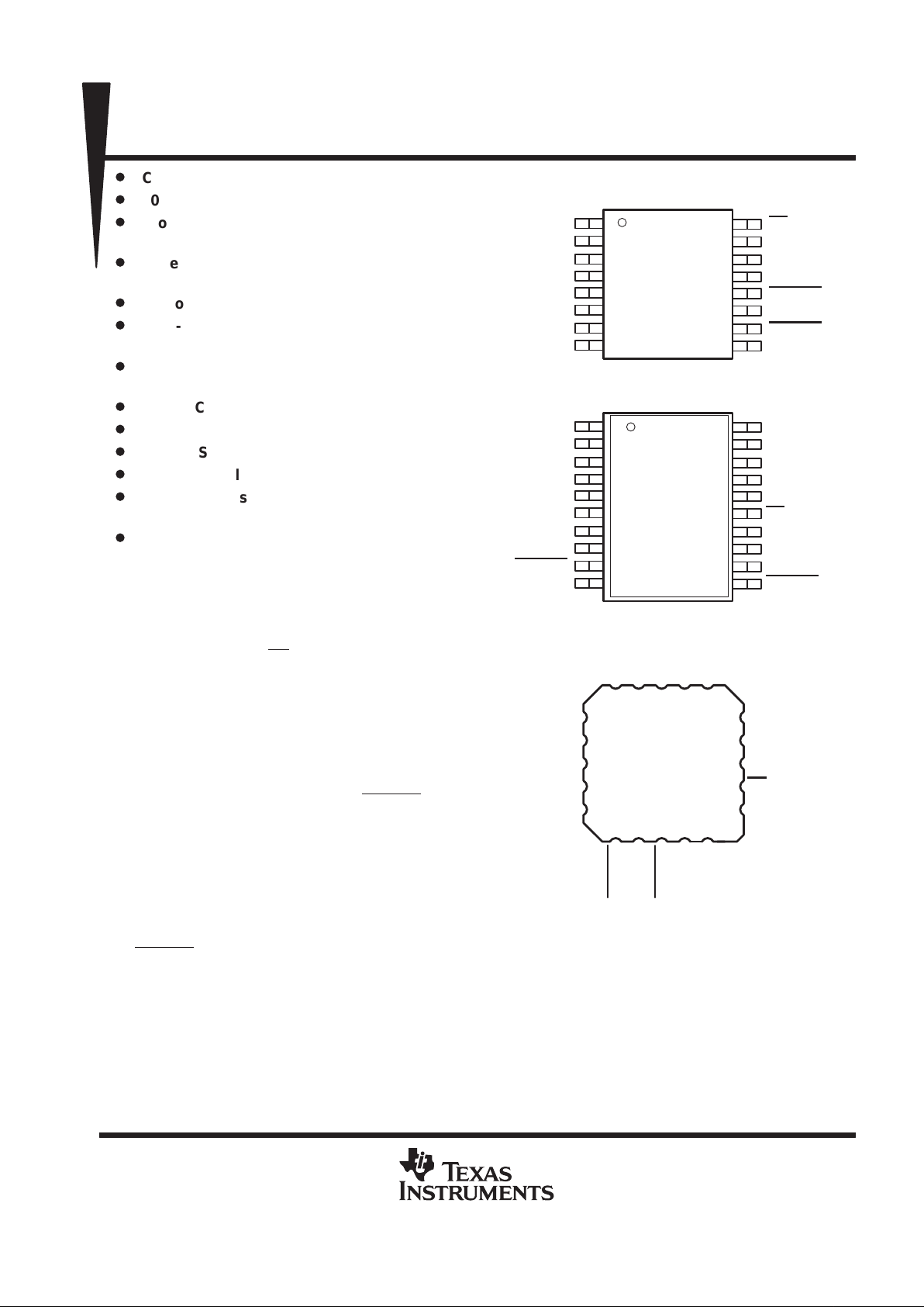
DB OR J PACKAGE
(TOP VIEW)
1
2
3
4
5
6
7
8
16
15
14
13
12
11
10
9
DATA OUT
DATA IN
I/O CLK
EOC
V
CC
A0
A1
A2
CS
REF+
REF–
FS
INV CLK
GND
CSTART
A3
D OR PW PACKAGE
(TOP VIEW)
1920132
17
18
16
15
14
1312119 10
5
4
6
7
8
I/O CLK
DATA IN
DATA OUT
CS
REF+
A3
A4
A5
A6
A7
A2A1A0VEOC
GND
INV CLK
FS
REF–
CSTART
FK PACKAGE
(TOP VIEW)
CC
PRODUCTION DATA information is current as of publication date.
Products conform to specifications per the terms of Texas Instruments
standard warranty. Production processing does not necessarily include
testing of all parameters.
Copyright 1999, Texas Instruments Incorporated
TLV1544C, TLV1544I, TLV1548C, TLV1548I, TLV1548M
LOW-VOLTAGE 10-BIT ANALOG-TO-DIGITAL CONVERTERS
WITH SERIAL CONTROL AND 4/8 ANALOG INPUTS
SLAS139C – DECEMBER 1996 – REVISED JANUARY 1999
2
POST OFFICE BOX 655303 • DALLAS, TEXAS 75265
description (continued)
The TLV1544 has four analog input channels while the TLV1548 has eight analog input channels. The
TL V1544C and TLV1548C are characterized for operation from 0°C to 70°C. The TLV1544I and TL V1548I are
characterized for operation over the full industrial temperature range of –40°C to 85°C. The TLV1548M is
characterized for operation over the full military temperature range of –55°C to 125°C.
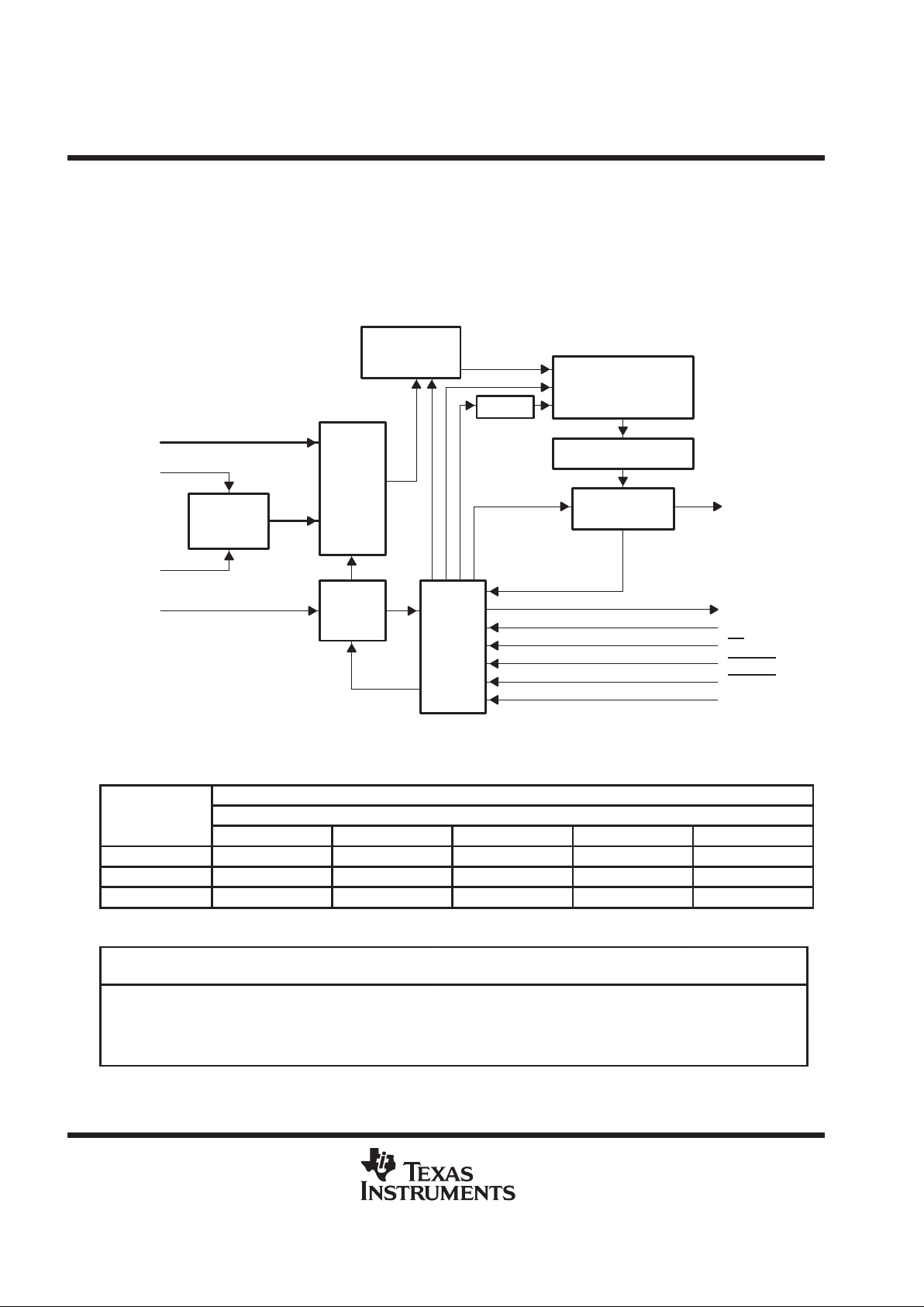
functional block diagram
Analog
MUX
Self-Test
Reference
Input
Data
Register
Control
Logic
and
I/O
Counters
10-Bit ADC
(Switch Capacitors)
Output Data Register
10-to-1
Data Selector
Sample
and
Hold Function
CLOCK
A0–A7
REF+
REF–
DATA IN
DATA OUT
EOC
FS
CS
CSTART
INV CLK
I/O CLK
Terminals shown are for the DB package.
1–8
14
13
17
16
19
12
15
9
11
18
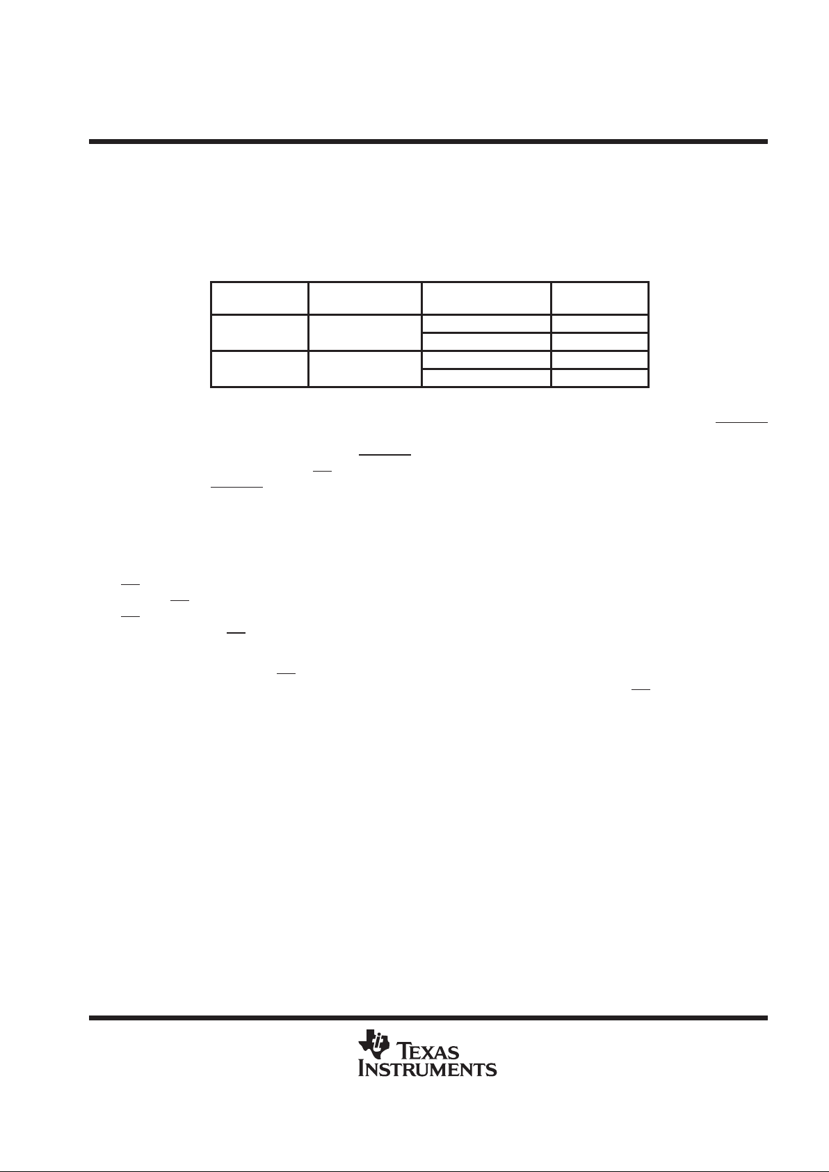
AVAILABLE OPTIONS
PACKAGE
T
A
SMALL OUTLINE
(DB) (D) (PW) (J) (FK)
0°C to 70°C TLV1548CDB TLV1544CD TLV1544CPW
–40°C to 85°C TLV1548IDB TLV1544ID TLV1544IPW
–55°C to 125°C TLV1548MJ TLV1548MFK
DISSIPATION RATING TABLE
T
≤ 25°C DERATING FACTOR
†
T
= 70°C T
= 85°C T
= 125°C
PACKAGE
A
POWER RATING ABOVE TA = 25°CAPOWER RATINGAPOWER RATINGAPOWER RATING
DB
785 mW
8.7 mW/°C
°
393 mW
261 mW
—
DPW799 mW
604 mW
8.9 mW/°C
6.7 mW/°C
399 mW
302 mW
266 mW
201 mW
—
—
JFK1894 mW
1375 mW
15.1 mW/°C
11.0 mW/°C
1212 mW
880 mW
985 mW
715 mW
379 mW
275 mW
†
This is the inverse of the traditional junction-to-ambient thermal resistance (RΘJA). RΘJA values are derived from T exas Instruments
characterization data. Thermal resistance is not production tested and values are given for informational purposes only .
TLV1544C, TLV1544I, TLV1548C, TLV1548I, TLV1548M
LOW-VOLTAGE 10-BIT ANALOG-TO-DIGITAL CONVERTERS
WITH SERIAL CONTROL AND 4/8 ANALOG INPUTS
SLAS139C – DECEMBER 1996 – REVISED JANUARY 1999
3
POST OFFICE BOX 655303 • DALLAS, TEXAS 75265
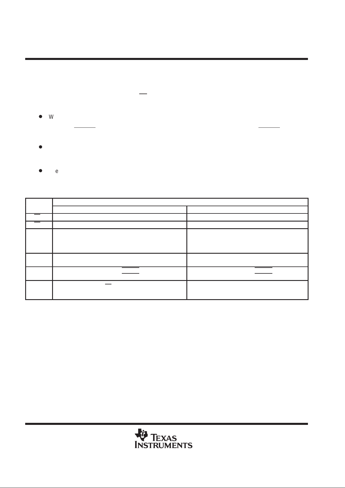
Terminal Functions
TERMINAL
NAME NO.†NO.
‡
I/O
DESCRIPTION
A0–A3
A4–A7
6–9–1–4
5–8
I Analog inputs. The analog inputs are internally multiplexed. (For a source impedance greater than
1 kΩ, the asynchronous start should be used to increase the sampling time.)
CS 16 15 I Chip select. A high-to-low transition on CS resets the internal counters and controls and enables DA T A IN,
DAT A OUT, and I/O CLK within the maximum setup time. A low-to-high transition disables DA TA IN, DA T A
OUT, and I/O CLK within the setup time.
CSTAR T 10 9 I Sampling/conversion start control. CSTART controls the start of the sampling of an analog input from a
selected multiplex channel. A high-to-low transition starts the sampling of the analog input signal. A
low-to-high transition puts the sample-and-hold function in hold mode and starts the conversion. CST ART
is independent from I/O CLK and works when CS is high. The low CSTAR T duration controls the duration
of the sampling cycle for the switched capacitor array. CSTART
is tied to VCC if not used.
DATA IN 2 17 I Serial data input. The 4-bit serial data selects the desired analog input and test voltage to be converted next
in a normal cycle. These bits can also set the conversion rate and enable the power-down mode.
When operating in the microprocessor mode, the input data is presented MSB first and is shifted in on the
first four rising (INV CLK
= VCC) or falling (INV CLK = GND) edges of I/O CLK (after CS↓).
g(
CC
)g( )g ( )
When operating in the DSP mode, the input data is presented MSB first and is shifted in on the first four
falling (INV CLK
= VCC) or rising (INV CLK = GND) edges of I/O CLK (after FS↓).
After the four input data bits have been read into the input data register, DA TA IN is ignored for the remainder
of the current conversion period.
DATA OUT 1 16 O Three-state serial output of the A/D conversion result. DA T A OUT is in the high-impedance state when CS
is high and active when CS is low or after FS↓ (in DSP mode). With a valid CS signal, DAT A OUT is removed
from the high-impedance state and is driven to the logic level corresponding to the MSB or LSB value of
the previous conversion result. DATA OUT changes on the falling (microprocessor mode) or rising (DSP
mode) edge of I/O CLK.
EOC 4 19 O End of conversion. EOC goes from a high to a low logic level on the tenth rising (microprocessor mode)
or tenth falling (DSP mode) edge of I/O CLK and remains low until the conversion is complete and data is
ready for transfer. EOC can also indicate that the converter is busy.
FS 13 12 I DSP frame synchronization input. FS indicates the start of a serial data frame into or out of the device. FS
is tied to VCC when interfacing the device with a microprocessor.
GND 11 10 Ground return for internal circuitry. All voltage measurements are with respect to GND, unless otherwise
noted.
INV CLK 12 11 I Inverted clock input. INV CLK is tied to GND when an inverted I/O CLK is used as the source of the input
clock. This affects both microprocessor and DSP interfaces. INV CLK
is tied to VCC if I/O CLK is not
inverted. INV CLK
can also invoke a built-in test mode.
†
Terminal numbers are for the D package.
‡
Terminal numbers are for the DB, J, and FK packages.
TLV1544C, TLV1544I, TLV1548C, TLV1548I, TLV1548M
LOW-VOLTAGE 10-BIT ANALOG-TO-DIGITAL CONVERTERS
WITH SERIAL CONTROL AND 4/8 ANALOG INPUTS
SLAS139C – DECEMBER 1996 – REVISED JANUARY 1999
4
POST OFFICE BOX 655303 • DALLAS, TEXAS 75265
Terminal Functions (Continued)
TERMINAL
NAME NO.†NO.
‡
I/O
DESCRIPTION
I/O CLK 3 18 I
Input/output clock. I/O CLK receives the serial I/O clock input in the two modes and performs the following
four functions in each mode:
Microprocessor mode
• When INVCLK = V
CC
, I/O CLK clocks the four input data bits into the input data register on the first four
rising edges of I/O CLK after CS
↓ with the multiplexer address available after the fourth rising edge.
When INV CLK
= GND, input data bits are clocked in on the first four falling edges instead.
• On the fourth falling edge of I/O CLK, the analog input voltage on the selected multiplex input begins
charging the capacitor array and continues to do so until the tenth rising edge of I/O CLK except in the
extended sampling cycle where the duration of CST ART
determines when to end the sampling cycle.
• Output data bits change on the first ten falling I/O clock edges regardless of the condition of INV CLK.
• I/O CLK transfers control of the conversion to the internal state machine on the tenth rising edge of I/O
CLK regardless of the condition of INV CLK
.
Digital signal processor (DSP) mode
• When INV CLK = V
CC
, I/O CLK clocks the four input data bits into the input data register on the first four
falling edges of I/O CLK after FS↓ with the multiplexer address available after the fourth falling edges.
When INV CLK
= GND, input data bits are clocked in on the first four rising edges instead.
• On the fourth rising edge of I/O CLK, the analog input voltage on the selected multiplex input begins
charging the capacitor array and continues to do so until the tenth falling edge of I/O CLK except in the
extended sampling cycle where the duration of CST ART
determines when to end the sampling cycle.
• Output data MSB shows after FS↓and the rest of the output data bits change on the first ten rising I/O
CLK edges regarless of the condition of INV CLK
.
• I/O CLK transfers control of the conversion to the internal state machine on the tenth falling edge of I/O
CLK regardless of the condition of INV CLK
.
REF+ 15 14 I Upper reference voltage (nominally VCC ). The maximum input voltage range is determined by the difference
between the voltages applied to REF+ and REF–.
REF– 14 13 I Lower reference voltage (nominally ground)
V
CC
5 20 I Positive supply voltage
†
Terminal numbers are for the D package.
‡
Terminal numbers are for the DB, J, and FK packages.
detailed description
Initially, with CS high (inactive), DATA IN and I/O CLK are disabled and DATA OUT is in the high-impedance
state. When the serial interface takes CS
low (active), the conversion sequence begins with the enabling of I/O
CLK and DAT A IN and the removal of DATA OUT from the high-impedance state. The host then provides the
4-bit channel address to DATA IN and the I/O clock sequence to I/O CLK. During this transfer, the host serial
interface also receives the previous conversion result from DA TA OUT . I/O CLK receives an input sequence from
the host that is from 10 to 16 clocks long. The first four valid I/O CLK cycles load the input data register with the
4-bit input data on DA TA IN that selects the desired analog channel. The next six clock cycles provide the control
timing for sampling the analog input. Sampling of the analog input is held after the first valid I/O CLK sequence
of ten clocks. The tenth clock edge also takes EOC low and begins the conversion. The exact locations of the
I/O clock edges depend on the mode of operation.
serial interface
The TL V1548 is compatible with generic microprocessor serial interfaces such as SPI and QSPI, and a TMS320
DSP serial interface. The internal latched flag If_mode is generated by sampling the state of FS at the falling
edge of CS
. If_mode is set to one (for microprocessor) when FS is high at the falling edge of CS, and If_mode
is cleared to zero (for DSP) when FS is low at the falling edge of CS
. This flag controls the multiplexing of I/O
CLK and the state machine reset function. FS is pulled high when interfacing with a microprocessor.
TLV1544C, TLV1544I, TLV1548C, TLV1548I, TLV1548M
LOW-VOLTAGE 10-BIT ANALOG-TO-DIGITAL CONVERTERS
WITH SERIAL CONTROL AND 4/8 ANALOG INPUTS
SLAS139C – DECEMBER 1996 – REVISED JANUARY 1999
5
POST OFFICE BOX 655303 • DALLAS, TEXAS 75265
I/O CLK
The I/O CLK can go up to 10 MHz for most of the voltage range when fast I/O is possible. The maximum I/O
CLK is limited to 2.8 MHz for a supply voltage range from 2.7 V . Table 1 lists the maximum I/O CLK frequencies
for all different supply voltage ranges. This also depends on input source impedance. For example, I/O CLK
speed faster than 2.39 MHz is achievable if the input source impedance is less than 1 kΩ.
Table 1. Maximum I/O CLK Frequency
V
CC
MAXIMUM INPUT
RESISTANCE (Max)
SOURCE IMPEDANCE I/O CLK
1 kΩ 2.39 MHz
2.7 V
5 K
100 Ω 2.81 MHz
1 kΩ 7.18 MHz
4.5 V
1 K
100 Ω 10 MHz
microprocessor serial interface
Input data bits from DATA IN are clocked in on the first four rising edges of the I/O CLK sequence if INV CLK
is held high when the device is in microprocessor interface mode. Input data bits are clocked in on the first four
falling edges of the I/O CLK sequence if INV CLK
is held low. The MSB of the previous conversion appears on
DA T A OUT on the falling edge of CS
. The remaining nine bits are shifted out on the next nine edges (depending
on the state of INV CLK
) of I/O CLK. Ten bits of data are transmitted to the host through DATA OUT.
A minimum of 9.5 clock pulses is required for the conversion to begin. On the tenth clock rising edge, the EOC
output goes low and returns to the high logic level when the conversion is complete; then the result can be read
by the host. On the tenth clock falling edge, the internal logic takes DA T A OUT low to ensure that the remaining
bit values are zero if the I/O CLK transfer is more than ten clocks long.
CS
is inactive (high) between serial I/O CLK transfers. Each transfer takes at least ten I/O CLK cycles. The falling
edge of CS
begins the sequence by removing DATA OUT from the high-impedance state. The rising edge of
CS
ends the sequence by returning DA TA OUT to the high-impedance state within the specified delay time. Also,
the rising edge of CS
disables I/O CLK and DA T A IN within a setup time. A conversion does not begin until the
tenth I/O CLK rising edge.
A high-to-low transition on CS
within the specified time during an ongoing cycle aborts the cycle, and the device
returns to the initial state (the output data register holds the previous conversion result). CS
should not be taken
low close to completion of conversion because the output data can be corrupted.
TLV1544C, TLV1544I, TLV1548C, TLV1548I, TLV1548M
LOW-VOLTAGE 10-BIT ANALOG-TO-DIGITAL CONVERTERS
WITH SERIAL CONTROL AND 4/8 ANALOG INPUTS
SLAS139C – DECEMBER 1996 – REVISED JANUARY 1999
6
POST OFFICE BOX 655303 • DALLAS, TEXAS 75265
DSP interface
The TL V1544/1548 can also interface with a DSP, from the TMS320 family for example, through a serial port.
The analog-to-digital converter (ADC) serves as a slave device where the DSP supplies FS and the serial I/O
CLK. Transmit and receive operations are concurrent. The falling edge of FS must occur no later than seven
I/O CLK periods after the falling edge of CS
.
DSP I/O cycles differ from microprocessor I/O cycles in the following ways:
D
When interfaced with a DSP , the output data MSB is available after FS↓. The remaining output data changes
on the rising edge of I/O CLK. The input data is sampled on the first four falling edges of I/O CLK after FS↓
and when INV CLK
is high, or the first four rising edges of I/O CLK after FS↓ and when INV CLK is low. This
operation is inverted when interfaced with a microprocessor.
D
A new DSP I/O cycle is started on the rising edge of I/O CLK after the rising edge of FS. The internal state
machine is reset on each falling edge of I/O CLK when FS is high. This operation is opposite when interfaced
with a microprocessor.
D
The TL V1544/1548 supports a 16-clock cycle when interfaced with a DSP. The output data is padded with
six trailing zeros when it is operated in DSP mode.
Table 2. TLV1544/TLV1548 Serial Interface Modes
INTERFACE MODE
I/O
MICROPROCESSOR ACTION DSP ACTION
CS↓ Initializes counter Samples state of FS
CS↑ Resets state machine and disable I/O Disables I/O
FS Connects to V
CC
Connects to DSP FSX output
Initializes the state machine at each CLK↓ after FS↑
Starts a new cycle at each CLK↑ following the initialization
(initializes the counter)
I/O CLK
Starts sampling of the analog input started at fourth I/O CLK↑
Conversion started at tenth I/O CLK↑
Starts sampling of the analog input at fourth I/O CLK↓
Starts sampling of the analog input at tenth I/O CLK↓
DATA IN
Samples input data on I/O CLK↑ (INV CLK high)
Samples input data on I/O CLK↓ (INV CLK
low)
Samples input data at I/O CLK↓ (INV CLK high)
Samples input data at I/O CLK↑ (INV CLK
low)
DATA OUT
Makes MSB available on CS↓
Changes remaining data on I/O CLK↓
Makes MSB available FS↓
Changes remaining data at each following I/O CLK↑ after
FS↓
TLV1544C, TLV1544I, TLV1548C, TLV1548I, TLV1548M
LOW-VOLTAGE 10-BIT ANALOG-TO-DIGITAL CONVERTERS
WITH SERIAL CONTROL AND 4/8 ANALOG INPUTS
SLAS139C – DECEMBER 1996 – REVISED JANUARY 1999
7
POST OFFICE BOX 655303 • DALLAS, TEXAS 75265
input data bits
DA TA IN is internally connected to a 4-bit serial input data register. The input data selects a different mode or
selects different analog input channels. The host provides the data word with the MSB first. Each data bit clocks
in on the edge (rising or falling depending on the status of INV CLK
and FS) of the I/O CLK sequence. The input
clock can be inverted by grounding INV CLK
(see Table 3 for the list of software programmed operations set
by the input data).
T able 3. TLV1544/1548 Software-Programmed Operation Modes
INPUT DATA BYTE
FUNCTION SELECT
A3 – A0
COMMENT
BINARY HEX
Analog channel A0 for TLV1548 selected 0000b 0h Channel 0 for TLV1544
Analog channel A1 for TLV1548 selected 0001b 1h
Analog channel A2 for TLV1548 selected 0010b 2h Channel 1 for TLV1544
Analog channel A3 for TLV1548 selected 0011b 3h
Analog channel A4 for TLV1548 selected 0100b 4h Channel 2 for TLV1544
Analog channel A5 for TLV1548 selected 0101b 5h
Analog channel A6 for TLV1548 selected 0110b 6h Channel 3 for TLV1544
Analog channel A7 for TLV1548 selected 011 1b 7h
Software power down set 1000b 8h No conversion result (cleared by any access)
Fast conversion rate (10 µs) set 1001b 9h No conversion result (cleared by setting to fast)
Slow conversion rate (40 µs) set 1010b Ah No conversion result (cleared by setting to slow)
Self-test voltage (V
ref
)
– V
ref–
)/2 selected 1011b Bh Output result = 200h
Self-test voltage V
ref
*
selected 1100b Ch Output result = 000h
Self-test voltage V
ref
)
selected 1101b Dh Output result = 3FFh
Reserved 1110b Eh No conversion result
Reserved 1111b Fh No conversion result
analog inputs and internal test voltages
The eight analog inputs and the three internal test inputs are selected by the 1 1-channel multiplexer according
to the input data bit as shown in Table 3. The input multiplexer is a break-before-make type to reduce
input-to-input noise injection resulting from channel switching.
The device can be operated in two distinct sampling modes: normal sampling mode (fixed sampling time) and
extended sampling mode (flexible sampling time). When CST ART
is held high, the device is operated in normal
sampling mode. When operated in normal sampling mode, sampling of the analog input starts on the rising edge
of the fourth I/O CLK pulse in the microprocessor interface mode (and on the fourth falling edge of I/O CLK in
the DSP interface mode). Sampling continues for 6 I/O CLK periods. The sample is held on the falling edge of
the tenth I/O CLK pulse in the microprocessor interface mode. The sample is held on the falling edge of the tenth
I/O CLK pulse in the DSP interface mode.The three test inputs are applied to the multiplexer, then sampled and
converted in the same manner as the external analog inputs.
TLV1544C, TLV1544I, TLV1548C, TLV1548I, TLV1548M
LOW-VOLTAGE 10-BIT ANALOG-TO-DIGITAL CONVERTERS
WITH SERIAL CONTROL AND 4/8 ANALOG INPUTS
SLAS139C – DECEMBER 1996 – REVISED JANUARY 1999
8
POST OFFICE BOX 655303 • DALLAS, TEXAS 75265
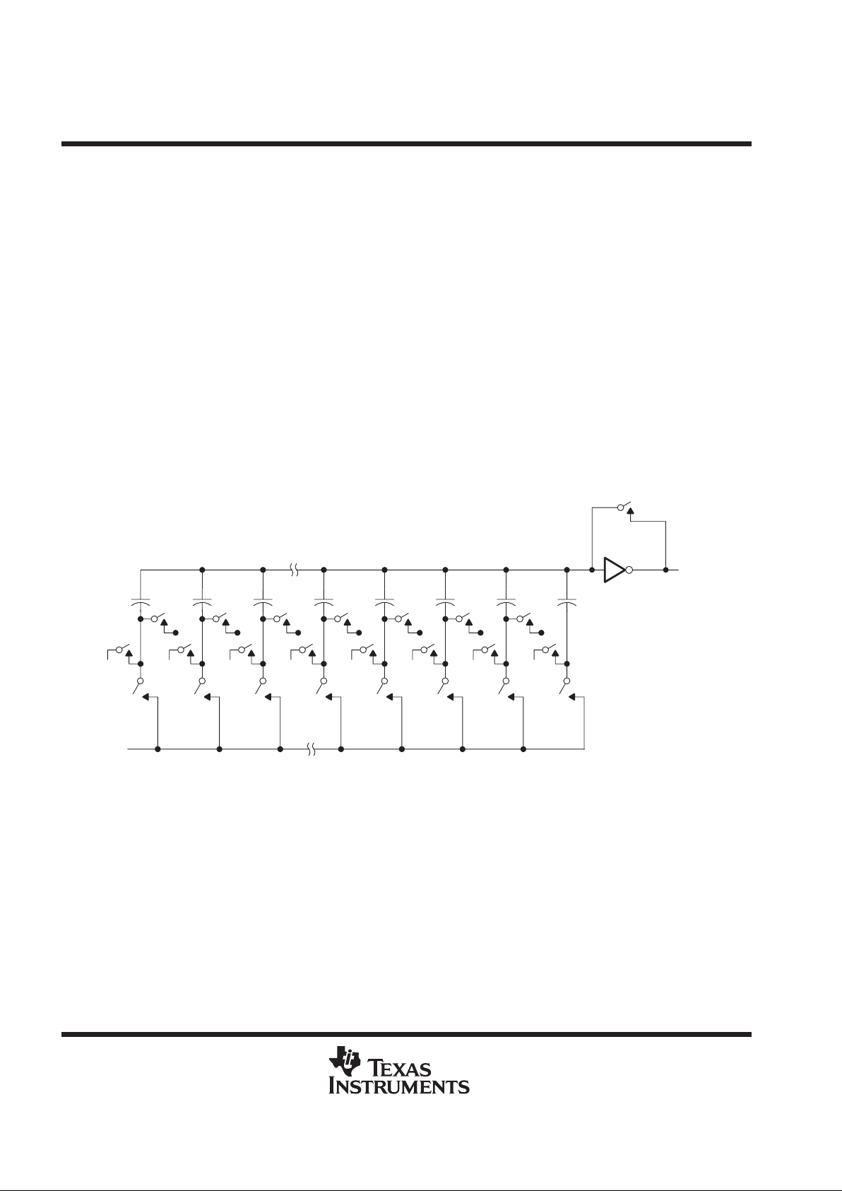
converter
The CMOS threshold detector in the successive-approximation conversion system determines the value of
each bit by examining the charge on a series of binary-weighted capacitors (see Figure 1). In the first phase
of the conversion process, the analog input is sampled by closing the S
C
switch and all ST switches
simultaneously. This action charges all of the capacitors to the input voltage.
In the next phase of the conversion process, all S
T
and SC switches are opened and the threshold detector
begins identifying bits by identifying the charge (voltage) on each capacitor relative to the reference (REF –)
voltage. In the switching sequence, ten capacitors are examined separately until all ten bits are identified and
then the charge-convert sequence is repeated. In the first step of the conversion phase, the threshold detector
looks at the first capacitor (weight = 512). Node 512 of this capacitor is switched to the REF+ voltage, and the
equivalent nodes of all the other capacitors on the ladder are switched to REF –. If the voltage at the summing
node is greater than the trip point of the threshold detector (approximately one-half V
CC
), a bit 0 is placed in the
output register and the 512-weight capacitor is switched to REF –. If the voltage at the summing node is less
than the trip point of the threshold detector, a bit 1 is placed in the register and the 512-weight capacitor remains
connected to REF + through the remainder of the successive-approximation process. The process is repeated
for the 256-weight capacitor, the 128-weight capacitor, and so forth down the line until all bits are counted.
With each step of the successive-approximation process, the initial charge is redistributed among the
capacitors. The conversion process relies on charge redistribution to count and weigh the bits from MSB to LSB.
S
C
Threshold
Detector
Node 512
REF–
REF+
S
T
512
V
I
To Output
Latches
REF–
S
T
REF+
REF–
S
T
REF+
REF–
S
T
REF+
REF–
S
T
REF+
S
T
REF+
REF–
S
T
REF+
REF–
S
T
11248128256
REF–
Figure 1. Simplified Model of the Successive-Approximation System
TLV1544C, TLV1544I, TLV1548C, TLV1548I, TLV1548M
LOW-VOLTAGE 10-BIT ANALOG-TO-DIGITAL CONVERTERS
WITH SERIAL CONTROL AND 4/8 ANALOG INPUTS
SLAS139C – DECEMBER 1996 – REVISED JANUARY 1999
9
POST OFFICE BOX 655303 • DALLAS, TEXAS 75265
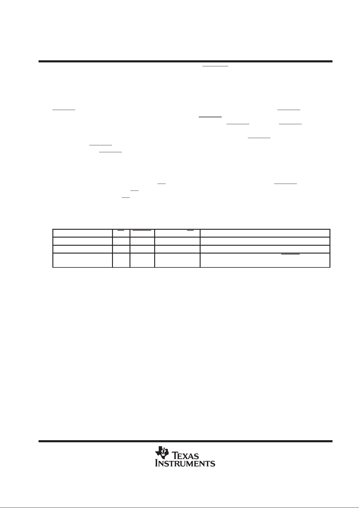
extended sampling, asynchronous start of sampling: CSTART operation
The extended sampling mode of operation programs the acquisition time (t
ACQ
) of the sample-and-hold circuit.
This allows the analog inputs of the device to be directly interfaced to a wide range of input source impedances.
The extended sampling mode consumes higher power depending on the duration of the sampling period
chosen.
CSTART
controls the sampling period and starts the conversion. The falling edge of CSTART initiates the
sampling period of a preset channel. The low time of CSTART
controls the acquisition time of the input
sample-and-hold circuit. The sample is held on the rising edge of CSTART
. Asserting CSTART causes the
converter to perform a new sample of the signal on the preset valid MUX channel (one of the eight) and discard
the current conversion result ready for output. Sampling continues as long as CST ART
is active (negative). The
rising edge of CST ART
ends the sampling cycle. The conversion cycle starts two internal system clocks after
the rising edge of CSTART
.
Once the conversion is complete, the processor can initiate a normal I/O cycle to read the conversion result and
set the MUX address for the next conversion. Since the internal flag AsyncFlag is set high, this flag setting
indicates the cycle is an output cycle, so no conversion is performed during the cycle. The internal state machine
tests the AsyncFlag on the falling edge of CS
. AsyncFlag is set high at the rising edge of CST ART , and it is reset
low at the rising edge of each CS
. A conversion cycle follows a sampling cycle only if AsyncFlag is tested as
low at the falling edge of CS
. As shown in Figure 2, an asynchronous I/O cycle can be removed by two
consecutive normal I/O cycles.
Table 4. TLV1544/1548 Hardware Configuration for Different Operating Modes
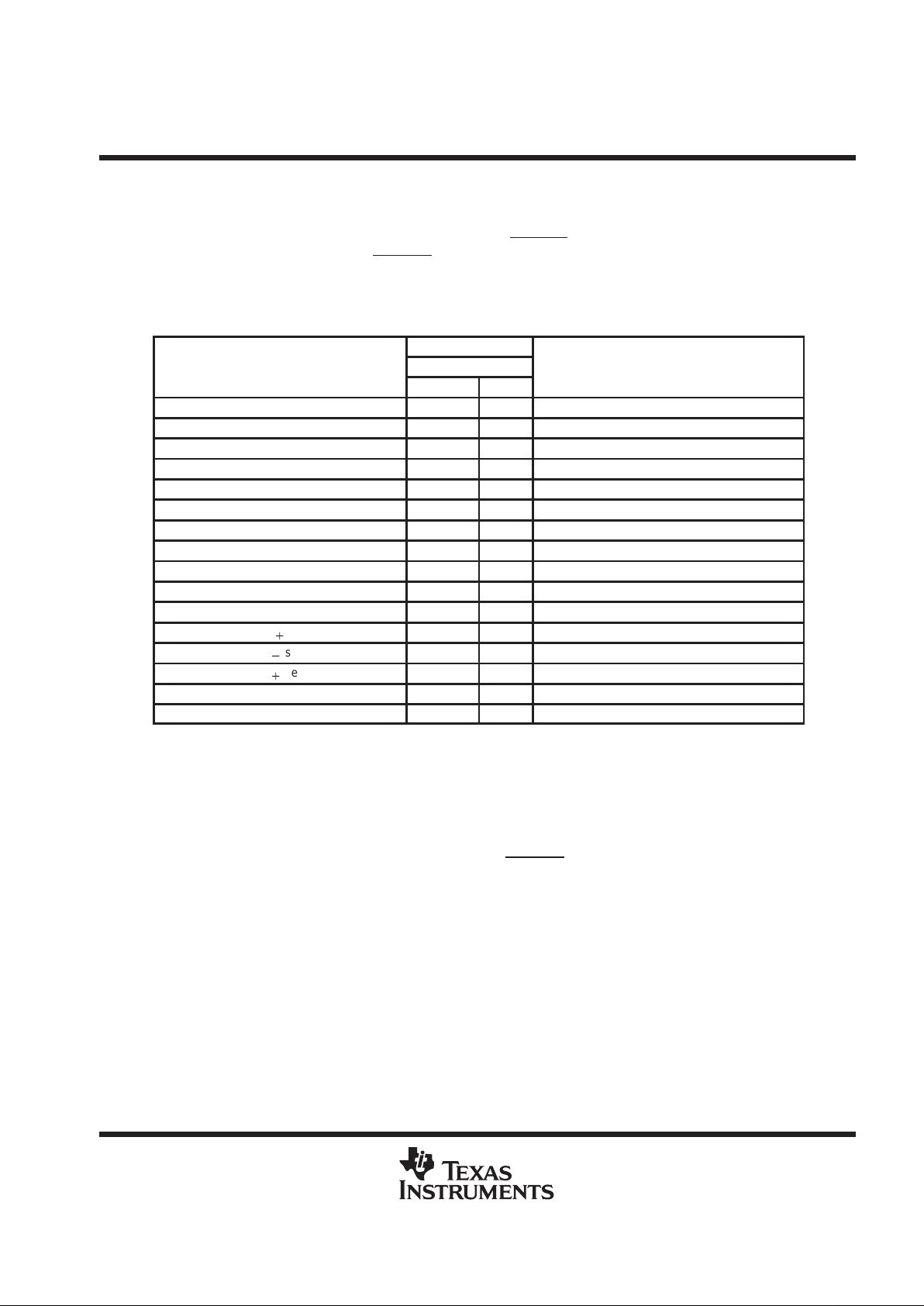
OPERATING MODES CS CSTART AsyncFlag at CS↓ ACTION
Normal sampling Low High Low Fixed 6 I/O CLK sampling, synchronous conversion follows
Normal I/O (read out only) Low High High No sampling, no conversion
Extended sampling High Low N/A
Flexible sampling period controlled by CSTAR T,
asynchronous conversion follows
TLV1544C, TLV1544I, TLV1548C, TLV1548I, TLV1548M
LOW-VOLTAGE 10-BIT ANALOG-TO-DIGITAL CONVERTERS
WITH SERIAL CONTROL AND 4/8 ANALOG INPUTS
SLAS139C – DECEMBER 1996 – REVISED JANUARY 1999
10
POST OFFICE BOX 655303 • DALLAS, TEXAS 75265
ООООООО
ООООООО
t
ACQ
Aa Ab Ab Ac Ad
XDaDb DbDc
CS
CSTART
DATA IN
EOC
DATA OUT
Async Flag
Read Out
Cycle
Read Out
Cycle
Read Out
Cycle
FS
(DSP Mode)
Complete Extended
Sample Cycle
t
ACQ
NOTES: A. Aa = Address for input channel a.
B. Da = Conversion result from channel a.
Hi–Z Hi–Z Hi–Z Hi–Z Hi–Z Hi–Z
Normal
Cycle
Normal
Cycle
Extended
Sample
Cycle
Extended
Sample
Cycle
Figure 2. Extended Sampling Operation
reference voltage inputs
There are two reference inputs used with the TLV1544/TLV1548, REF+ and REF–. These voltage values
establish the upper and lower limits of the analog inputs to produce a full-scale and zero-scale reading
respectively . The values of REF+, REF–, and the analog input should not exceed the positive supply or be lower
than GND consistent with the specified absolute maximum ratings. The digital output is at full scale when the
input signal is equal to or higher than REF+ and is at zero when the input signal is equal to or lower than REF–.
programmable conversion rate
The TL V1544/TLV1548 offers two conversion rates to maximize battery life when high-speed operation is not
necessary . The conversion rate is programmable. Once the conversion rate has been selected, it takes ef fect
immediately in the same cycle and stays at the same rate until the other rate is chosen. The conversion rate
should be set at power up. Activation and deactivation of the power-down state (digital logic active) has no effect
on the preset conversion rate.
TLV1544C, TLV1544I, TLV1548C, TLV1548I, TLV1548M
LOW-VOLTAGE 10-BIT ANALOG-TO-DIGITAL CONVERTERS
WITH SERIAL CONTROL AND 4/8 ANALOG INPUTS
SLAS139C – DECEMBER 1996 – REVISED JANUARY 1999
11
POST OFFICE BOX 655303 • DALLAS, TEXAS 75265
Table 5. Conversion Rate and Power Consumption Selection
TYPICAL SUPPL Y CURRENT, I
CC
CONVERSION RATE
CONVERSION TIME
,
t
conv
AVAILABLE V
CC
RANGE
INPUT DATA
OPERATING
POWER
DOWN
Fast conversion speed 7 µs typ 5.5 V to 3.3 V 9h 0.6 mA typ 1.5 mA max 1 µA typ
Slow conversion speed 15 µs typ 5.5 V to 2.7 V Ah 0.4 mA typ 1 mA max 1 µA typ
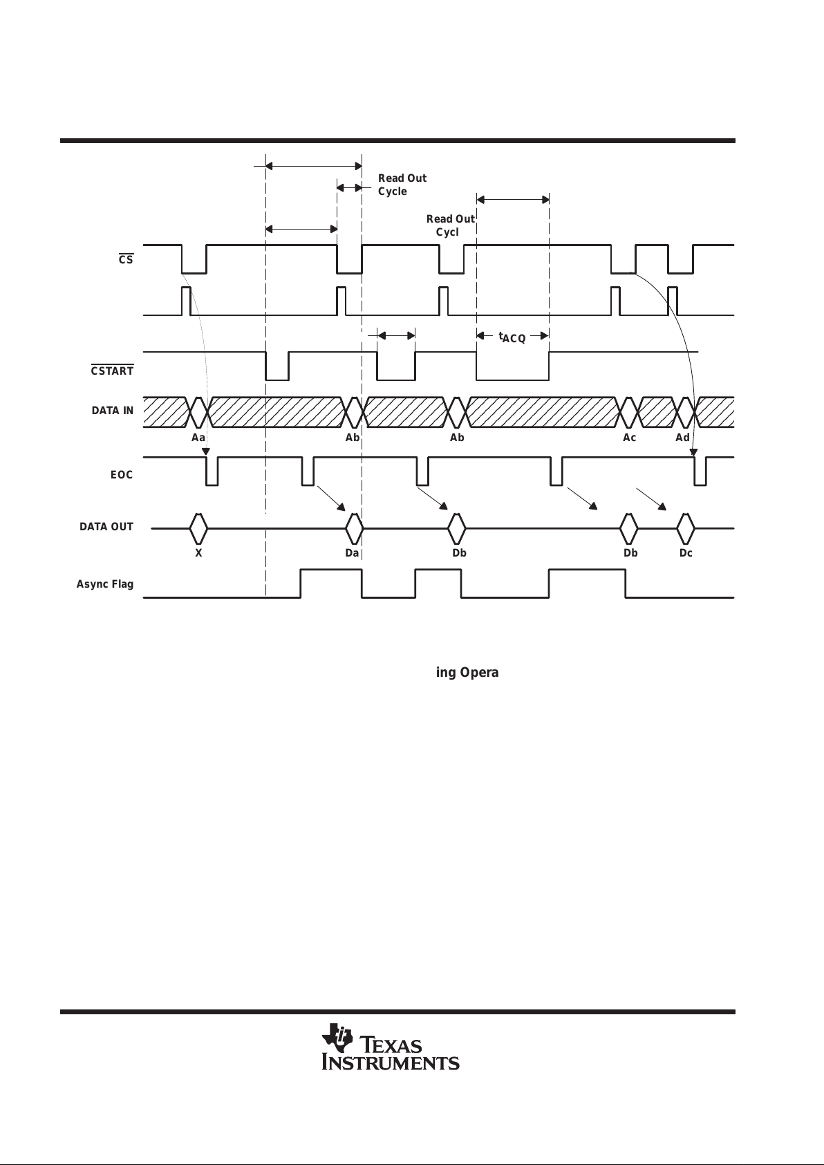
programmable power-down state
The device is put into the power-down state by writing 8h to DATA IN. The power-up state is restored during
the next active access by pulling CS
low. The conversion rate selected before the device is put into the
power-down state is not affected by the power-down mode. Power-down can be used to achieve even lower
power consumption. This is because the sustaining power (when not converting) is only 1.3 mA maximum and
standby power is only 1 µA maximum. (By averaging out the power consumption can be much lower than the
1 mA peak when the conversion throughput is lower.)
Power Down
CS
EOC
I
CC
DATA IN
Hi-Z Hi-Z
0
Supply Current
1 000
1 mA
(Typical Peak Supply)
0.3 mA
(Typical Sustaining)
0.0007 mA
(Typical Power Down
Supply)
Figure 3. Typical Supply Current During Conversion/Power Down
power up and initialization
After power up, if operating in DSP mode, CS and FS must be taken from high to low to begin an I/O cycle. EOC
is initially high, and the input data register is set to all zeroes. The content of the output data register is random,
and the first conversion result should be ignored. For initialization during operation, CS
is taken high and
returned low to begin the next I/O cycle. The first conversion after the device has returned from the power-down
state can be invalid and should be disregarded.
When power is first applied to the device, the conversion rate must be programmed, and the internal Async Flag
must be taken low once. The rising edge of CS
of the same cycle then takes Async Flag low.
TLV1544C, TLV1544I, TLV1548C, TLV1548I, TLV1548M
LOW-VOLTAGE 10-BIT ANALOG-TO-DIGITAL CONVERTERS
WITH SERIAL CONTROL AND 4/8 ANALOG INPUTS
SLAS139C – DECEMBER 1996 – REVISED JANUARY 1999
12
POST OFFICE BOX 655303 • DALLAS, TEXAS 75265
9h 0h Ab
X
D0
MUX Address for Channel 0
AsyncFlag Reset LowConversion Rate Set to Fast
Conversion Result From Channel 0
CS
DATA IN
DATA OUT
EOC
Signal Channel 0 Converted
FS
(For DSP Mode)
First Cycle After Powerup
Async Flag
(Internal)
Hi–Z Hi–Z Hi–Z Hi–Z
X
Figure 4. Power Up Initialization
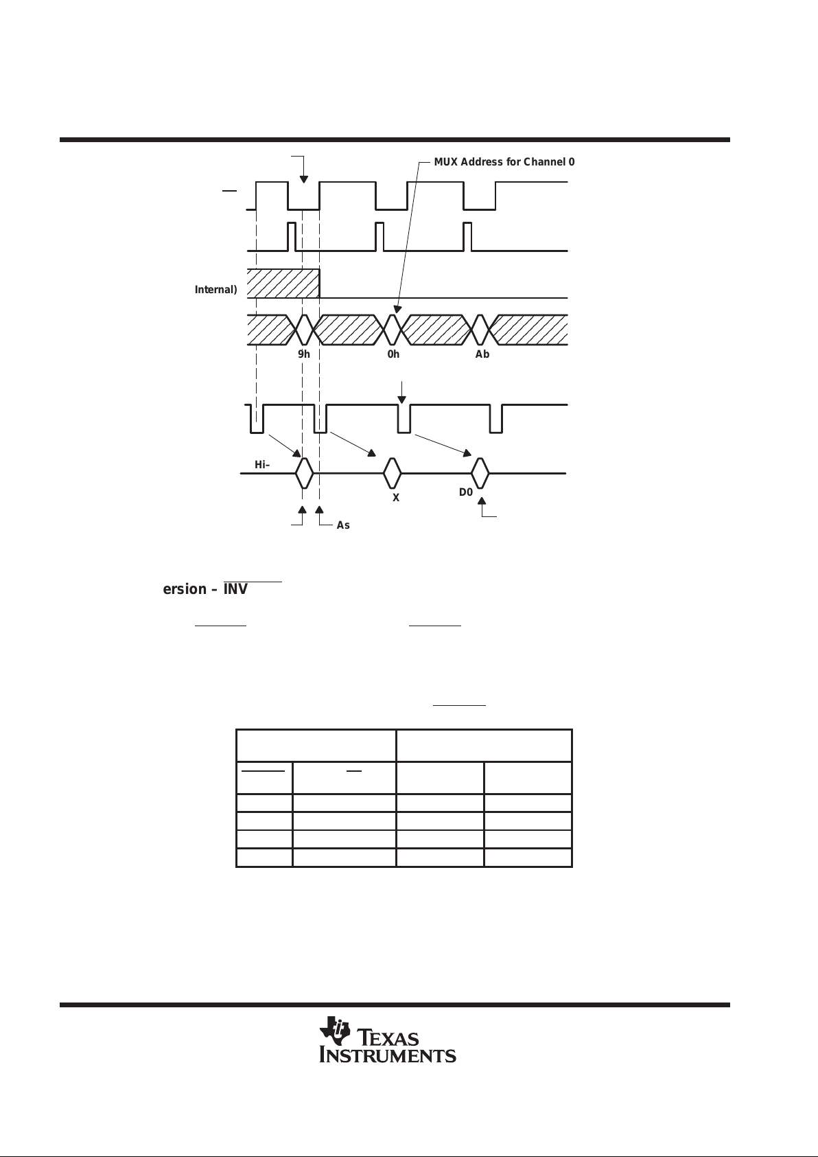
input clock inversion – INV CLK
The input data register uses I/O CLK as the source of the sampling clock. This clock can be inverted to provide
more setup time. INV CLK
can invert the clock. When INV CLK is grounded, the input clock for the input data
register is inverted. This allows an additional one-half I/O CLK period for the input data setup time. This is useful
for some serial interfaces. When the input sampling clock is inverted, the output data changes at the same time
that the input data is sampled.
Table 6. Function of INV CLK
CONDITION
CLOCK
I/O CLK ACTIVE EDGE
INV CLK FS at CS↓
OUTPUT DATA
CHANGES ON
INPUT DATA
SAMPLED ON
High High (MP† mode) ↓ ↑
High Low (DSP‡ mode) ↑ ↓
Low High (MP† mode) ↓ ↓
Low Low (DSP‡ mode) ↑ ↑
†
MP = microprocessor mode
‡
DSP = digital signal processor mode

TLV1544C, TLV1544I, TLV1548C, TLV1548I, TLV1548M
LOW-VOLTAGE 10-BIT ANALOG-TO-DIGITAL CONVERTERS
WITH SERIAL CONTROL AND 4/8 ANALOG INPUTS
SLAS139C – DECEMBER 1996 – REVISED JANUARY 1999
13
POST OFFICE BOX 655303 • DALLAS, TEXAS 75265
11-to-1
Analog
MUX
Input
Data
Register
2-to-1
Sample-
andHold
Function
SAR† Latch
Threshold
Detect
10-to-1 Select
Output Shift Clock
Conversion
Clock
OSC
Invert
2-to-1
If_mode
Input Shift Clock
DSP
§
SMCLK
Control
State
Machine
If_mode
If_mode
Invert
EOC
DATA OUT
INV CLK
CS
FS
I/O CLK
REF+
REF–
A0–A7
TEST 0–2
DATA IN
V
ref
REF+
REF–
Microprocessor
‡
†
Successive approximation register
‡
If_mode = 1, microprocessor interface mode
§
If_mode = 0, DSP interface mode
Figure 5. Clock Scheme
absolute maximum ratings over operating free-air temperature range (unless otherwise noted)
†
Supply voltage range, V
CC
(see Note 1) –0.5 V to 6.5 V. . . . . . . . . . . . . . . . . . . . . . . . . . . . . . . . . . . . . . . . . . . . .
Input voltage range, V
I
(any input) –0.3 V to VCC + 0.3 V. . . . . . . . . . . . . . . . . . . . . . . . . . . . . . . . . . . . . . . . . . . .
Output voltage range, V
O
–0.3 V to VCC + 0.3 V. . . . . . . . . . . . . . . . . . . . . . . . . . . . . . . . . . . . . . . . . . . . . . . . . . .
Positive reference voltage, V
ref+
V
CC
+ 0.1 V. . . . . . . . . . . . . . . . . . . . . . . . . . . . . . . . . . . . . . . . . . . . . . . . . . . . . .
Negative reference voltage, V
ref–
–0.1 V. . . . . . . . . . . . . . . . . . . . . . . . . . . . . . . . . . . . . . . . . . . . . . . . . . . . . . . . . .
Peak input current, I
I
(any input) ±20 mA. . . . . . . . . . . . . . . . . . . . . . . . . . . . . . . . . . . . . . . . . . . . . . . . . . . . . . . . . .
Peak total input current (all inputs) –30 mA. . . . . . . . . . . . . . . . . . . . . . . . . . . . . . . . . . . . . . . . . . . . . . . . . . . . . . . .
Operating free-air temperature range, T
A
: TL V1544C, TLV1548C 0°C to 70°C. . . . . . . . . . . . . . . . . . . . . . . .
TLV1544I, TLV1548I –40°C to 85°C. . . . . . . . . . . . . . . . . . . . . . . .
TLV1548M –55°C to 125°C. . . . . . . . . . . . . . . . . . . . . . . . . . . . . . . .
Storage temperature range, T
stg
–65°C to 150°C. . . . . . . . . . . . . . . . . . . . . . . . . . . . . . . . . . . . . . . . . . . . . . . . . . .
Lead temperature 1,6 mm (1/16 inch) from the case for 10 seconds 260°C. . . . . . . . . . . . . . . . . . . . . . . . . . . .
†
Stresses beyond those listed under “absolute maximum ratings” may cause permanent damage to the device. These are stress ratings only, and
functional operation of the device at these or any other conditions beyond those indicated under “recommended operating conditions” is not
implied. Exposure to absolute-maximum-rated conditions for extended periods may affect device reliability.
NOTE 1: All voltage values are with respect to GND with REF– and GND wired together (unless otherwise noted).

TLV1544C, TLV1544I, TLV1548C, TLV1548I, TLV1548M
LOW-VOLTAGE 10-BIT ANALOG-TO-DIGITAL CONVERTERS
WITH SERIAL CONTROL AND 4/8 ANALOG INPUTS
SLAS139C – DECEMBER 1996 – REVISED JANUARY 1999
14
POST OFFICE BOX 655303 • DALLAS, TEXAS 75265
recommended operating conditions
MIN NOM MAX UNIT
Supply voltage, V
CC
2.7 5.5 V
Positive reference voltage, V
ref+
(see Note 2) V
CC
V
Negative reference voltage, V
ref–
(see Note 2) 0 V
Differential reference voltage, V
ref+
– V
ref–
(see Note 2) 2.5 V
CCVCC
+0.2 V
Analog input voltage, VI
(analog)
(see Note 2) 0 V
CC
V
High-level control input voltage, V
IH
2.1 V
Low-level control input voltage, V
IL
0.6 V
Setup time, input data bits valid before I/O CLK↑↓, t
su(A)
(see Figure 9) 100 ns
Hold time, input data bits valid after I/O CLK↑↓, t
h(A)
(see Figure 9) 5 30 ns
Setup time, CS↓ to I/O CLK↑, t
su(CS)
See Figure 10 5 30 ns
Hold time, I/O CLK↓ to CS↑, t
h(CS)
See Figure 10 65 ns
Pulse duration, FS high, t
wH(FS)
See Figure 12 1
I/O CLK
periods
Pulse duration, CSTAR T, t
w(CSTART)
Source impedance ≤ 1 kΩ, VCC = 5.5 V,
See Figure 14
0.84 µs
Setup time, CS↑ to CSTART↓, t
su(CSTART)
See Figure 14 10 ns
VCC = 5.5 V 0.1 6 10
Clock frequency at I/O CLK, f
CLK
VCC = 2.7 V 0.1 2 2.81
MH
z
VCC = 5.5 V 50
Pulse duration, I/O CLK high, t
wH(I/O)
VCC = 2.7 V 100
ns
VCC = 5.5 V 50
Pulse duration, I/O CLK lo
w,
t
wL(I/O)
VCC = 2.7 V 100
ns
Transition time, I/O CLK, t
t(I/O)
(see Figure 11 and Note 4) 1 µs
Transition time, DATA IN, t
t(DATA IN)
(see Figure 9) 10 µs
Transition time, CS, t
t(CS)
(see Figure 10) 10 µs
Transition time, FS, t
t(FS)
(see Figure 13) 10 µs
Transition time, CSTART, t
t(CSTAR T)
(see Figure 14) 10 µs
TLV1544C, TLV1548C 0 70
Operating free-air temperature, T
A
TLV1544I, TLV1548I –40 85
°C
TLV1548M –55 125
TLV1544C, TLV1548C 115
Junction temperature, T
J
TLV1544I, TLV1548I 115
°C
TLV1548M 150
NOTES: 2. Analog input voltages greater than the voltage applied to REF+ convert as all ones (111111111111), while input voltages less than
the voltage applied to REF– convert as all zeros (000000000000). The device is functional with reference (V
ref+
– V
ref–
) down to 1
V; however , the electrical specifications are no longer applicable.
3. To minimize errors caused by noise at CS
↓, the internal circuitry waits for a setup time after CS↓before responding to control input
signals. No attempt should be made to clock in an input dat until the minimum CS
setup time has elapsed.
4. This is the time required for the I/O CLK signal to fall from VIHmax to VILmin or to rise from VILmax to VIHmin. In the vicinity of normal
room temperature, the devices function with an input clock transition time as slow as 1 µs for remote data-acquisition applications
where the sensor and the A/D converter are placed several feet away from the controlling microprocessor.

TLV1544C, TLV1544I, TLV1548C, TLV1548I, TLV1548M
LOW-VOLTAGE 10-BIT ANALOG-TO-DIGITAL CONVERTERS
WITH SERIAL CONTROL AND 4/8 ANALOG INPUTS
SLAS139C – DECEMBER 1996 – REVISED JANUARY 1999
15
POST OFFICE BOX 655303 • DALLAS, TEXAS 75265
electrical characteristics over recommended operating free-air temperature range,
V
CC
= V
ref+
= 2.7 V to 5.5 V, I/O CLK frequency = 2.2 MHz (unless otherwise noted)
PARAMETER TEST CONDITIONS MIN TYP†MAX UNIT
p
VCC = 5.5 V, IOH = –0.2 mA 2.4
VOHHigh-level output voltage
VCC = 2.7 V, IOH = –20 µA V
CC–0.1
V
p
VCC = 5.5 V, IOL = 0.8 mA 0.4
VOLLow-level output voltage
VCC = 2.7 V, IOL = 20 µA 0.1
V
p
p
VO = VCC, CS = V
CC
1 2.5
IOZHigh-impedance output current
VO = 0, CS = V
CC
–1 –2.5
µ
A
I
IH
High-level input current VI = V
CC
0.005 2.5 µA
I
IL
Low-level input current VI = 0 –0.005 2.5 µA
Conversion speed = fast,
For all digital inputs,
0 ≤ VI ≤ 0.3 V or
VI ≥ VCC – 0.3 V
VCC = 3.3 V to 5.5 V 0.6 1.5
ICCO
perating supply curren
t
Conversion speed = slow,
For all di
g
ital inputs,
VCC = 3.3 V to 5.5 V 0.4 1
m
A
g,
0 ≤ VI ≤ 0.3 V or
VI ≥ VCC – 0.3 V
VCC = 2.7 V to 3.3 V 0.35 0.75
Extended sampling mode
VCC = 3.3 V to 5.5 V 1.5 mA
I
CC(ES)
g
operating current
VCC = 2.7 V to 3.3 V
1 mA
I
CC(ST)
Sustaining supply current
Conversion speed = slow,
For all digital inputs,
0 ≤ VI ≤ 0.3 V or
VI ≥ VCC – 0.3 V
VCC = 2.7 V to 3.3 V 0.3 mA
I
CC(PD)
Power-down supply current
For all digital inputs,
0 ≤ VI ≤ 0.3 V or VI ≥ VCC – 0.3 V
1 25 µA
Selected channel at VCC, unselected channel at 0 V 1 µA
I
lkg
Selected channel leakage current
Selected channel at 0 V , unselected channel at V
CC
–1 µA
Maximum static analog
reference current into REF+
V
ref+
= VCC = 5.5 V, V
ref–
= GND 1 µA
Input capacitance, analog inputs 20 55
p
C
i
‡
Input capacitance, control inputs 20 15
pF
p
p
VCC = 4.5 V 1
Z
i
‡
Input multiplexer on resistance
VCC = 2.7 V 5
kΩ
†
All typical values are at VCC = 5 V, TA = 25°C.
‡
Not production tested.

TLV1544C, TLV1544I, TLV1548C, TLV1548I, TLV1548M
LOW-VOLTAGE 10-BIT ANALOG-TO-DIGITAL CONVERTERS
WITH SERIAL CONTROL AND 4/8 ANALOG INPUTS
SLAS139C – DECEMBER 1996 – REVISED JANUARY 1999
16
POST OFFICE BOX 655303 • DALLAS, TEXAS 75265
operating characteristics over recommended operating free-air temperature range,
V
CC
= V
ref+
= 2.7 V to 5.5 V, I/O CLK frequency = 2.2 MHz (unless otherwise noted)
PARAMETER
TEST
CONDITIONS
MIN TYP
†
MAX UNIT
E
L
Linearity error (see Note 6) ±0.5 ±1 LSB
E
D
Differential linearity error See Note 2 ±0.5 ±1 LSB
E
O
Offset error (see Note 7) See Note 2 ±1.5 LSB
E
G
Gain error (see Note 7) See Note 2 ±1 LSB
E
T
Total unadjusted error (see Note 8) ±1.75 LSB
DATA IN = 1011 512
Self-test output code (see Table 3 and Note 9)
DATA IN - 1100 0
DATA IN = 1101 1023
Fast conversion speed
See Figures 15
7 10 µs
t
conv
Conversion time
Slow conversion speed
g
through 17
15 25 µs
Total cycle time (access,
p
Fast conversion speed
See Figures 15
through 18 and
Notes 10, 11, 12
10.1 +
10 I/O CLK
t
c
sample, conversion and
EOC↑
to CS↓ delay)
Slow conversion speed
See Figures 15
through 18 and
Notes 10 and 12
40.1 +
10 I/O CLK
µ
s
t
acq
Channel acquisition time (sample)
See Figures 15
through 18 and
Note 10
6
I/O CLK
periods
t
v
Valid time, DATA OUT remains valid after I/O CLK↓ See Figure 11 50 ns
t
d1(FS)
Delay time, I/O CLK high to FS high See Figure 13 5 30 50 ns
t
d2(FS)
Delay time, I/O CLK high to FS low See Figure 13 10 30 60 ns
t
d(EOC↑ – CS↓)
Delay time, EOC↑ to CS low
See Figure 14
and Note 5
100 ns
t
d(CS↓ – FS↑)
Delay time, CS↓ to FS↑
See Figures 17
and 18
1 7
I/O CLK
periods
t
d(I/O -CS)
Delay time, 10th I/O CLK low to CS low to abort
conversion (see Note 13)
See Figure 10 1.1 µs
†
All typical values are at TA = 25°C.
NOTES: 2. Analog input voltages greater than that applied to REF+ convert as all ones (111111111111), while input voltages less than that
applied to REF– convert as all zeros (000000000000). The device is functional with reference down to 1 V (V
ref
+ – V
ref
– 1); however,
the electrical specifications are no longer applicable.
5. For all operating modes.
6. Linearity error is the maximum deviation from the best straight line through the A/D transfer characteristics.
7. Zero error is the difference between 0000000000 and the converted output for zero input voltage. Full-scale error is the difference
between 1111111111 and the converted output for full-scale input voltage.
8. Total unadjusted error comprises linearity, zero-scale, and full-scale errors.
9. Both the input data and the output codes are expressed in positive logic.
10. I/O CLK period = 1/(I/O CLK frequency) (see Figure 8).
11. For 3.3 V to 5.5 V only
12. For microprocessor mode
13. Any transitions of CS
are recognized as valid only when the level is maintained for a setup time after the transition.

TLV1544C, TLV1544I, TLV1548C, TLV1548I, TLV1548M
LOW-VOLTAGE 10-BIT ANALOG-TO-DIGITAL CONVERTERS
WITH SERIAL CONTROL AND 4/8 ANALOG INPUTS
SLAS139C – DECEMBER 1996 – REVISED JANUARY 1999
17
POST OFFICE BOX 655303 • DALLAS, TEXAS 75265
operating characteristics over recommended operating free-air temperature range,
V
CC
= V
ref+
= 2.7 V to 5.5 V, I/O CLK frequency = 2.2 MHz (unless otherwise noted) (continued)
PARAMETER TEST CONDITIONS MIN TYP†MAX UNIT
t
d(I/O-DATA)
Delay time, I/O CLK low to DATA OUT valid See Figure 11 50 ns
t
d(I/O-EOC)
Delay time, 10th I/O CLK↓ to EOC low See Figure 12 70 240 ns
t
PZH
, t
PZL
Enable time, CS low to DATA OUT valid (MSB driven) See Figure 8 0.7 1.3 µs
t
PHZ
, t
PLZ
Disable time, CS high to DATA OUT invalid (high impedance) See Figure 8 70 150 ns
t
f(EOC)
Fall time, EOC See Figure 12 15 50 ns
t
r(bus)
Rise time, output data bus at 2.2 MHz I/O CLK See Figure 11 50 250 ns
t
f(bus)
Fall time, output data bus at 2.2 MHz I/O CLK See Figure 11 50 250 ns
†
All typical values are at TA = 25°C.
PARAMETER MEASUREMENT INFORMATION
_
+
C2
0.1 µF
C1
10 µF
15 V
–15 V
V
I
Ax
TLV1544/48
U1
C1
10 µF
C2
0.1 µF
LOCATION
U1
C1
C2
DESCRIPTION
OP27
10-µF 35-V tantalum capacitor
0.1-µF ceramic NPO SMD capacitor
PART NUMBER
—
—
AVX 12105C104KA105 or equivalent
EOC
D0
Figure 6. Analog Input Buffer to Analog Inputs
EOC
CL = 50 pF
12 kΩ
DATA OUT
Test Point
V
CC
RL = 2.18 kΩ
CL = 100 pF
12 kΩ
Test Point
V
CC
RL = 2.18 kΩ
Figure 7. Load Circuits

TLV1544C, TLV1544I, TLV1548C, TLV1548I, TLV1548M
LOW-VOLTAGE 10-BIT ANALOG-TO-DIGITAL CONVERTERS
WITH SERIAL CONTROL AND 4/8 ANALOG INPUTS
SLAS139C – DECEMBER 1996 – REVISED JANUARY 1999
18
POST OFFICE BOX 655303 • DALLAS, TEXAS 75265
PARAMETER MEASUREMENT INFORMATION
CS
DATA
OUT
90%
10%
90%
10%
t
PZH
, t
PZL
t
PHZ
, t
PLZ
10%
90%
Figure 8. DATA OUT to Hi-Z Voltage Waveforms
V
IH
V
IL
V
OH
V
OL
DATA IN
t
h(A)
10%
90%
I/O CLK
Address
Valid
t
su(A)
10%
Figure 9. DATA IN Setup Voltage Waveforms
tt
(DATA IN)
tt
(DATA IN)
t
t(I/O)
10% 10%10%
90%
V
IH
V
IL
V
IH
V
IL
Last
Clock
CS
10%
90%
10%
t
su(CS)
10%
I/O CLK
t
h(CS)
t
d(I/O-CS)
First
Clock
90%
t
t(CS)
t
t(CS)
10%
V
IH
V
IL
V
IL
Figure 10. CS and I/O CLK Voltage Waveforms
10%
90%
10%
90%
90%
10%
I/O CLK
DATA OUT
t
t(I/O)
10%
90%
t
r(bus)
, t
f(bus)
t
d(I/O-DATA)
t
v
t
t(I/O)
10%
I/O Clock Period
V
IH
V
IL
V
OH
V
OL
VALID
Figure 11. DATA OUT and I/O CLK Voltage Waveforms
CS
t
d(ES–FS
FS
Figure 12. CS Low to FS Low

TLV1544C, TLV1544I, TLV1548C, TLV1548I, TLV1548M
LOW-VOLTAGE 10-BIT ANALOG-TO-DIGITAL CONVERTERS
WITH SERIAL CONTROL AND 4/8 ANALOG INPUTS
SLAS139C – DECEMBER 1996 – REVISED JANUARY 1999
19
POST OFFICE BOX 655303 • DALLAS, TEXAS 75265
PARAMETER MEASUREMENT INFORMATION
10th
Clock
10%
I/O CLK
EOC
(µp Mode)
10%
V
IL
V
OH
V
OL
90%
10%
t
f(EOC)
t
d(I/O-EOC)
V
OH
V
OL
t
d(I/O-EOC)
10%
EOC
(DSP Mode)
Figure 13. I/O CLK and EOC Voltage Waveforms
t
d1(FS)
I/O CLK
FS
90%
90%
10%
90%
t
t(FS)
t
t(FS)
10%
V
IH
V
IL
90%
t
d2(FS)
V
IH
V
IL
t
wH(FS)
Figure 14. FS and I/O CLK Voltage Waveforms
CS
t
su(CSTART)
t
d(EOC↑-CS↓)
CSTART
EOC
10%
10%
10% 10%
V
IL
t
d(I/O-EOC)
V
OL
t
w(CSTART)
90%
t
t(CSTART)
90%
t
t(CSTART)
Figure 15. CSTART and CS Waveforms

TLV1544C, TLV1544I, TLV1548C, TLV1548I, TLV1548M
LOW-VOLTAGE 10-BIT ANALOG-TO-DIGITAL CONVERTERS
WITH SERIAL CONTROL AND 4/8 ANALOG INPUTS
SLAS139C – DECEMBER 1996 – REVISED JANUARY 1999
20
POST OFFICE BOX 655303 • DALLAS, TEXAS 75265
PARAMETER MEASUREMENT INFORMATION
t
d(EOC↑-CS↓)
NOTE A: T o minimize errors caused by noise at CS, the internal circuitry waits for a setup time after CS↓ before responding to control input
signals. No attempt should be made to clock in input data until the minimum CS
setup time elapses.
1 2 3 4 5 6 7 8 9 10
I/O CLK
Conversion
Sample
(6 I/O CLKs)
DI
DO
EOC
CS
MSB
MSB LSB
D9 D8 D7 D6 D5 D4 D3 D2 D1 D0
Hi-ZHi-Z
A3 A2 A1 A0
Rise After 10th I/O CLK↓
(see Note A)
Address Sampled
Initialize State Machine
and Counter
Access
Conversion Starts on 10th I/O CLK↑
0s
A
3
D
9
Figure 16. Microprocessor Interface Timing (Normal Sample Mode, INV CLK = High)
NOTE A: T o minimize errors caused by noise at CS, the internal circuitry waits for a setup time after CS↓ before responding to control input
signals. No attempt should be made to clock in input data until the minimum CS
setup time has elapsed.
t
d(EOC↑-CS↓)
1 2 3 45678910
I/O CLK
Conversion
Sample
DI
DO
EOC
CS
MSB
MSB LSB
D9 D8 D7 D6 D5 D4 D3 D2 D1 D0
Hi-ZHi-Z
A2 A1 A0
Rise After 10th I/O CLK↓
(see Note A)
Address Sampled
Conversion Starts on 10th I/O CLK↑
Initialize State Machine
and Counter
(5.5 I/O CLKs)
Access
0s
A
3
D
9
A3
Figure 17. Microprocessor Interface Timing (Normal Sample Mode, INV CLK = Low)

TLV1544C, TLV1544I, TLV1548C, TLV1548I, TLV1548M
LOW-VOLTAGE 10-BIT ANALOG-TO-DIGITAL CONVERTERS
WITH SERIAL CONTROL AND 4/8 ANALOG INPUTS
SLAS139C – DECEMBER 1996 – REVISED JANUARY 1999
21
POST OFFICE BOX 655303 • DALLAS, TEXAS 75265
PARAMETER MEASUREMENT INFORMATION
NOTE A: T o minimize errors caused by noise at CS, the internal circuitry waits for a setup time after CS↓ before responding to control input
signals. No attempt should be made to clock in input data until the minimum CS
setup time elapses.
I/O CLK
DI
DO
EOC
CS
(see
Note A)
FS
1
2 3 45678910
Sample
MSB
MSB LSB
D9 D8 D7 D6 D5 D4 D3 D2 D1 D0
Hi-ZHi-Z
A3 A2 A1 A0
Address Sampled
Conversion Starts on 10th I/O CLK↓
(6 I/O CLKs)
Access
11 12 13 14 15
16
Hold/Conversion
CS Rise After 16th I/O CLK↓
Initialize Counter
0s
t
d(EOC↑-CS↓)
Initialize State Machine
7 I/O CLKs
Maximum
Figure 18. DSP Interface Timing (16-Clock Transfer, Normal Sample Mode, INV CLK = High)

TLV1544C, TLV1544I, TLV1548C, TLV1548I, TLV1548M
LOW-VOLTAGE 10-BIT ANALOG-TO-DIGITAL CONVERTERS
WITH SERIAL CONTROL AND 4/8 ANALOG INPUTS
SLAS139C – DECEMBER 1996 – REVISED JANUARY 1999
22
POST OFFICE BOX 655303 • DALLAS, TEXAS 75265
PARAMETER MEASUREMENT INFORMATION
NOTE A: T o minimize errors caused by noise at CS, the internal circuitry waits for a setup time after CS↓ before responding to control input
signals. No attempt should be made to clock in input data until the minimum CS
setup time elapses.
I/O CLK
DI
DO
EOC
CS
(see
Note A)
FS
ООООООООООООООООООООО
1
2 3 45678910
Sample
MSB
MSB LSB
D9 D8 D7 D6 D5 D4 D3 D2 D1 D0
Hi-ZHi-Z
A3 A2 A1 A0
Address Sampled
Conversion Starts on 10th I/O CLK↓
(6 I/O CLKs)
Access
11 12 13 14 15
16
Hold/Conversion
CS Rise After 16th I/O CLK↓
Initialize Counter
0s
t
d(EOC↑-CS↓)
Initialize State Machine
7 I/O CLKs
Maximum
Figure 19. DSP Interface Timing (16-Clock Transfer, Normal Sample Mode, INV CLK = Low)

TLV1544C, TLV1544I, TLV1548C, TLV1548I, TLV1548M
LOW-VOLTAGE 10-BIT ANALOG-TO-DIGITAL CONVERTERS
WITH SERIAL CONTROL AND 4/8 ANALOG INPUTS
SLAS139C – DECEMBER 1996 – REVISED JANUARY 1999
23
POST OFFICE BOX 655303 • DALLAS, TEXAS 75265
TYPICAL CHARACTERISTICS
Figure 20
TA – Free-Air Temperature – °C
0
–0.2
–0.4
–75 25 125
INL – Integral Nonlinearity Error – LSB
INTEGRAL NONLINEARITY ERROR
vs
FREE-AIR TEMPERATURE
0.1
–0.1
0.2
0.4
0.3
–0.3
–25 75
Maximum
Minimum
VCC = 2.7 V
Figure 21
TA – Free-Air Temperature – °C
0.4
0.3
0.2
0.1
–0.1
–0.3
–0.4
–0.5
–75 25 125
0.5
INTEGRAL NONLINEARITY ERROR
vs
FREE-AIR TEMPERATURE
–0.2
INL – Integral Nonlinearity Error – LSB
75–25
VCC = 5.5 V
Maximum
Minimum
0
Figure 22
DNL – Differential Nonlinearity Error – LSB
DIFFERENTIAL NONLINEARITY ERROR
vs
FREE-AIR TEMPERATURE
TA – Free-Air Temperature – °C
0
–0.2
–0.5
–75 25 125
0.1
–0.1
0.2
0.4
0.3
–0.3
–25 75
VCC = 2.7 V
Maximum
Minimum
–0.4
Figure 23
DIFFERENTIAL NONLINEARITY ERROR
vs
FREE-AIR TEMPERATURE
DNL – Differential Nonlinearity Error – LSB
TA – Free-Air Temperature – °C
0
–0.6
–75 25
0.2
0.6
0.4
–0.2
–25 75
VCC = 5.5 V
Maximum
Minimum
–0.4
125

TLV1544C, TLV1544I, TLV1548C, TLV1548I, TLV1548M
LOW-VOLTAGE 10-BIT ANALOG-TO-DIGITAL CONVERTERS
WITH SERIAL CONTROL AND 4/8 ANALOG INPUTS
SLAS139C – DECEMBER 1996 – REVISED JANUARY 1999
24
POST OFFICE BOX 655303 • DALLAS, TEXAS 75265
TYPICAL CHARACTERISTICS
Figure 24
– Offset Error – LSB
OFFSET ERROR
vs
FREE-AIR TEMPERATURE
E
O
TA – Free-Air Temperature – °C
0.2
0.1
0
–75 25 125
0.15
0.25
0.35
0.3
0.05
–25 75
VCC = 2.7 V
VCC = 5.5 V
Figure 25
GAIN ERROR
vs
FREE-AIR TEMPERATURE
– Gain Error – LSBE
G
TA – Free-Air Temperature – °C
0.4
0.2
0
–75 25 125
0.3
0.5
0.7
0.6
0.1
–25 75
VCC = 2.7 V
VCC = 5.5 V
Figure 26
– Total Unadjusted Error – LSB
TOTAL UNADJUSTED ERROR
vs
FREE-AIR TEMPERATURE
E
T
TA – Free-Air Temperature – °C
0.2
0
–0.2
–75 25 125
0.1
0.3
0.8
0.4
–0.1
–25 75
Maximum
Minimum
0.5
0.6
0.7
VCC = 2.7 V
Figure 27
TOTAL UNADJUSTED ERROR
vs
FREE-AIR TEMPERATURE
– Total Unadjusted Error – LSBE
T
TA – Free-Air Temperature – °C
0.2
0
–0.4
–75 25 125
–0.2
1.2
0.4
–25 75
Maximum
Minimum
0.6
0.8
1
VCC = 5.5 V

TLV1544C, TLV1544I, TLV1548C, TLV1548I, TLV1548M
LOW-VOLTAGE 10-BIT ANALOG-TO-DIGITAL CONVERTERS
WITH SERIAL CONTROL AND 4/8 ANALOG INPUTS
SLAS139C – DECEMBER 1996 – REVISED JANUARY 1999
25
POST OFFICE BOX 655303 • DALLAS, TEXAS 75265
TYPICAL CHARACTERISTICS
– Supply Current – mA
SUPPLY CURRENT
vs
FREE-AIR TEMPERATURE
I
CC
TA – Free-Air Temperature – °C
0.46
0.44
0.4
–75 25 125
0.42
0.56
0.48
–25 75
0.5
0.52
0.54
VCC = 5.5 V
Clock Mode =
Fast Conversion
Figure 28
Figure 29
Digital Output Code
1.6
1.2
0.8
0.4
0
0 512 1023
INL – Integral Nonlinearity Error – LSB
VCC = 2.7 V
TA = 25°C
Clock Mode = Fast
–0.4
–0.8
–1.2
–1.6
INTEGRAL NONLINEARITY ERROR
vs
DIGITAL OUTPUT CODE
2
–2
Figure 30
Digital Output Code
2
1
0
0 512 1023
Differential Nonlinearity Error – LSB
–1
–2
DIFFERENTIAL NONLINEARITY ERROR
vs
DIGITAL OUTPUT CODE
VCC = 2.7 V
TA = 25°C
Clock Mode = Fast

TLV1544C, TLV1544I, TLV1548C, TLV1548I, TLV1548M
LOW-VOLTAGE 10-BIT ANALOG-TO-DIGITAL CONVERTERS
WITH SERIAL CONTROL AND 4/8 ANALOG INPUTS
SLAS139C – DECEMBER 1996 – REVISED JANUARY 1999
26
POST OFFICE BOX 655303 • DALLAS, TEXAS 75265
TYPICAL CHARACTERISTICS
Figure 31
0
–0.2
–0.6
–1
0 512
0.4
0.8
INTEGRAL NONLINEARITY ERROR
vs
DIGITAL OUTPUT CODE
1
1023
VCC = 5 V
TA = –40°C
Clock Mode = Fast
0.6
0.2
–0.4
–0.8
Digital Output Code
INL – Integral Nonlinearity Error – LSB
Figure 32
0
–0.2
–0.6
–1
0 512
0.4
0.8
DIFFERENTIAL NONLINEARITY ERROR
vs
DIGITAL OUTPUT CODE
1
1023
0.6
0.2
–0.4
–0.8
Digital Output Code
DNL – Differential Nonlinearity Error – LSB
VCC = 5 V
TA = –40°C
Clock Mode = Fast
Figure 33
0
–0.2
–0.6
–1
0 512
0.4
0.8
INTEGRAL NONLINEARITY ERROR
vs
DIGITAL OUTPUT CODE
1
1023
0.6
0.2
–0.4
–0.8
Digital Output Code
INL – Integral Nonlinearity Error – LSB
VCC = 5 V
TA = 25°C
Clock Mode = Fast
Figure 34
0
–0.2
–0.6
–1
0 512
0.4
0.8
DIFFERENTIAL NONLINEARITY ERROR
vs
DIGITAL OUTPUT CODE
1
1023
0.6
0.2
–0.4
–0.8
Digital Output Code
DNL – Differential Nonlinearity Error – LSB
VCC = 5 V
TA = 25°C
Clock Mode = Fast

TLV1544C, TLV1544I, TLV1548C, TLV1548I, TLV1548M
LOW-VOLTAGE 10-BIT ANALOG-TO-DIGITAL CONVERTERS
WITH SERIAL CONTROL AND 4/8 ANALOG INPUTS
SLAS139C – DECEMBER 1996 – REVISED JANUARY 1999
27
POST OFFICE BOX 655303 • DALLAS, TEXAS 75265
TYPICAL CHARACTERISTICS
Figure 35
0
–0.2
–0.6
–1
0 512
0.4
0.8
INTEGRAL NONLINEARITY ERROR
vs
DIGITAL OUTPUT CODE
1
1023
VCC = 5 V
TA = 85°C
Clock Mode = Fast
0.6
0.2
–0.4
–0.8
Digital Output Code
INL – Integral Nonlinearity Error – LSB
Figure 36
0
–0.2
–0.6
–1
0 512
0.4
0.8
DIFFERENTIAL NONLINEARITY ERROR
vs
DIGITAL OUTPUT CODE
1
1023
0.6
0.2
–0.4
–0.8
Digital Output Code
DNL – Differential Nonlinearity Error – LSB
VCC = 5 V
TA = 85°C
Clock Mode = Fast

TLV1544C, TLV1544I, TLV1548C, TLV1548I, TLV1548M
LOW-VOLTAGE 10-BIT ANALOG-TO-DIGITAL CONVERTERS
WITH SERIAL CONTROL AND 4/8 ANALOG INPUTS
SLAS139C – DECEMBER 1996 – REVISED JANUARY 1999
28
POST OFFICE BOX 655303 • DALLAS, TEXAS 75265
APPLICATION INFORMATION
1000000000
0111111111
0000000010
0000000001
0000000000
1111111110
0 0.0096 2.4528 2.4576 2.4624
Digital Output Code
1000000001
1111111101
1111111111
4.9128 4.9140 4.9152
512
511
2
1
0
1022
Step
513
1021
1023
0.0024
VI – Analog Input Voltage – V
VZT = VZS + 1/2 LSB
V
ZS
See Notes A and B
4.9080
0.0048
VFT = VFS – 1/2 LSB
V
FS
V
FSnom
NOTES: A. This curve is based on the assumption that V
ref+
and V
ref–
have been adjusted so that the voltage at the transition from digital 0
to 1 (VZT) is 0.0024 V , and the transition to full scale (VFT) is 4.908 V. 1 LSB = 4.8 mV.
B. The full-scale value (VFS) is the step whose nominal midstep value has the highest absolute value. The zero-scale value (VZS) is
the step whose nominal midstep value equals zero.
Figure 37. Ideal Conversion Characteristics

TLV1544C, TLV1544I, TLV1548C, TLV1548I, TLV1548M
LOW-VOLTAGE 10-BIT ANALOG-TO-DIGITAL CONVERTERS
WITH SERIAL CONTROL AND 4/8 ANALOG INPUTS
SLAS139C – DECEMBER 1996 – REVISED JANUARY 1999
29
POST OFFICE BOX 655303 • DALLAS, TEXAS 75265
APPLICATION INFORMATION
I/O 2
CLKX
CLKR
DX
DR
Microprocessor
15
18
17
16
14
13
10
3 V dc
Regulated
20
12
CS
I/O CLK
DATA IN
DATA OUT
REF+
REF–
GND
A0–A7
V
CC
FS
V
CC
Analog Inputs
To Source Ground
1–8
TLV1548
†
11
INV CLK
†
DB package is shown for TLV1548
Figure 38. Typical Interface to a Microprocessor
IO2
CLKX
CLKR
DX
DR
TMS320 DSP
15
18
17
16
12
CS
I/O CLK
DATA IN
DATA OUT
FS
A0–A7
Analog Inputs
1–8
FSX
FSR
TLV1548
‡
20
V
CC
V
CC
11
INV CLK
REF+
REF–
GND
To Source GND
3 V dc
Regulated
‡
DB package is shown for TLV1548
10
13
14
Figure 39. Typical Interface to a TMS320 DSP

TLV1544C, TLV1544I, TLV1548C, TLV1548I, TLV1548M
LOW-VOLTAGE 10-BIT ANALOG-TO-DIGITAL CONVERTERS
WITH SERIAL CONTROL AND 4/8 ANALOG INPUTS
SLAS139C – DECEMBER 1996 – REVISED JANUARY 1999
30
POST OFFICE BOX 655303 • DALLAS, TEXAS 75265
APPLICATIONS INFORMATION
simplified analog input analysis
Using the equivalent circuit in Figure 33, the time required to charge the analog input capacitance from 0 to V
S
within 1/2 LSB can be derived as follows:
The capacitance charging voltage is given by:
where
R
t
= Rs + r
i
tc = Cycle time
VC+
V
S
ǒ
1–e
–tcń
RtC
i
Ǔ
The input impedance Zi is 1 kΩ at 5 V , and is higher (~ 5 k Ω) at 2.7 V. The final voltage to 1/2 LSB is given by:
V
C
(1/2 LSB) = VS – (VS/2048)
Equating equation 1 to equation 2 and solving for cycle time t
c
gives:
and time to change to 1/2 LSB (minimum sampling time) is:
t
ch
(1/2 LSB) = Rt × Ci × ln(2048)
VS*
ǒ
VSń
2048Ǔ+
V
S
ǒ
1–e
–tcń
RtC
i
Ǔ
where
ln(2048) = 7.625
Therefore, with the values given, the time for the analog input signal to settle is:
t
ch
(1/2 LSB) = (Rs + 1 kΩ) × 55 pF × ln(2048)
This time must be less than the converter sample time shown in the timing diagrams. Which is 6x I/O CLK.
t
ch
(1/2 LSB) ≤ 6x 1/f
I/O
Therefore the maximum I/O CLK frequency is:
max(f
I/O
) = 6/tch (1/2 LSB) = 6/(ln(2048) × Rt × Ci)
(1)
(2)
(3)
(4)
(5)
(6)

TLV1544C, TLV1544I, TLV1548C, TLV1548I, TLV1548M
LOW-VOLTAGE 10-BIT ANALOG-TO-DIGITAL CONVERTERS
WITH SERIAL CONTROL AND 4/8 ANALOG INPUTS
SLAS139C – DECEMBER 1996 – REVISED JANUARY 1999
31
POST OFFICE BOX 655303 • DALLAS, TEXAS 75265
APPLICATIONS INFORMATION
R
s
r
i
V
S
V
C
55 pF MAX
1 kΩ
Driving Source
†
TLV1544/48
C
i
V
I
VI= Input Voltage at AIN
VS= External Driving Source Voltage
Rs= Source Resistance
ri= Input Resistance (MUX on Resistance)
Ci= Input Capacitance
VC= Capacitance Charging Voltage
†
Driving source requirements:
• Noise and distortion for the source must be equivalent to the resolution of the converter.
• Rs must be real at the input frequency.
Figure 40. Equivalent Input Circuit Including the Driving Source
maximum conversion throughput
For a supply voltage at 5 V,
if the source impedance is less than 1 kΩ, this equates to a minimum sampling
time t
ch
(0.5 LSB) of 0.84 µs. Since the sampling time requires six I/O clocks, the fastest I/O clockfrequency is
6/t
ch
= 7.18 MHz. The minimal total cycle time is given as:
t
c
= t
address
+ t
sample
+ t
conv
+ t
d(EOC↑ – CS↓)
= 0.56 µs + 0.84 µs + 10 µs + 0.1 µs
= 11.5 µs
A maximum throughput of 87 KSPS. The throughput can be even higher with a smaller source impedance.
When source impedance is 100Ω, the minimum sampling time is 0.46 µs. The maximum I/O clock frequency
possible is almost 13 MHz. Then 10 MHz clock (maximum I/O CLK for TL V1544/1548) can be used. The minimal
total cycle time is:
t
c
= t
address
+ t
sample
+ t
conv
+ t
d(EOC↑ – CS↓)
= 4 × 1/f + 0.46 µs + 10 µs + 0.1 µs
= 0.4 µs + 0.46 µs + 10 µs + 0.1 µs
= 10.96 µs
The maximum throughput is 1/10.96 µs = 91 KSPS for this case.

TLV1544C, TLV1544I, TLV1548C, TLV1548I, TLV1548M
LOW-VOLTAGE 10-BIT ANALOG-TO-DIGITAL CONVERTERS
WITH SERIAL CONTROL AND 4/8 ANALOG INPUTS
SLAS139C – DECEMBER 1996 – REVISED JANUARY 1999
32
POST OFFICE BOX 655303 • DALLAS, TEXAS 75265
MECHANICAL DATA
D (R-PDSO-G**) PLASTIC SMALL-OUTLINE PACKAGE
14 PIN SHOWN
4040047/D 10/96
0.228 (5,80)
0.244 (6,20)
0.069 (1,75) MAX
0.010 (0,25)
0.004 (0,10)
1
14
0.014 (0,35)
0.020 (0,51)
A
0.157 (4,00)
0.150 (3,81)
7
8
0.044 (1,12)
0.016 (0,40)
Seating Plane
0.010 (0,25)
PINS **
0.008 (0,20) NOM
A MIN
A MAX
DIM
Gage Plane
0.189
(4,80)
(5,00)
0.197
8
(8,55)
(8,75)
0.337
14
0.344
(9,80)
16
0.394
(10,00)
0.386
0.004 (0,10)
M
0.010 (0,25)
0.050 (1,27)
0°–8°
NOTES: A. All linear dimensions are in inches (millimeters).
B. This drawing is subject to change without notice.
C. Body dimensions do not include mold flash or protrusion, not to exceed 0.006 (0,15).
D. Falls within JEDEC MS-012

TLV1544C, TLV1544I, TLV1548C, TLV1548I, TLV1548M
LOW-VOLTAGE 10-BIT ANALOG-TO-DIGITAL CONVERTERS
WITH SERIAL CONTROL AND 4/8 ANALOG INPUTS
SLAS139C – DECEMBER 1996 – REVISED JANUARY 1999
33
POST OFFICE BOX 655303 • DALLAS, TEXAS 75265
MECHANICAL DATA
DB (R-PDSO-G**) PLASTIC SMALL-OUTLINE PACKAGE
4040065 /D 02/98
28 PIN SHOWN
Gage Plane
8,20
7,40
0,15 NOM
0,63
1,03
0,25
38
12,90
12,30
28
10,50
24
8,50
Seating Plane
9,907,90
30
10,50
9,90
0,38
5,60
5,00
15
0,22
14
A
28
1
2016
6,50
6,50
14
0,05 MIN
5,905,90
DIM
A MAX
A MIN
PINS **
2,00 MAX
6,90
7,50
0,65
M
0,15
0°–8°
0,10
NOTES: A. All linear dimensions are in millimeters.
B. This drawing is subject to change without notice.
C. Body dimensions do not include mold flash or protrusion not to exceed 0,15.
D. Falls within JEDEC MO-150

TLV1544C, TLV1544I, TLV1548C, TLV1548I, TLV1548M
LOW-VOLTAGE 10-BIT ANALOG-TO-DIGITAL CONVERTERS
WITH SERIAL CONTROL AND 4/8 ANALOG INPUTS
SLAS139C – DECEMBER 1996 – REVISED JANUARY 1999
34
POST OFFICE BOX 655303 • DALLAS, TEXAS 75265
MECHANICAL DATA
FK (S-CQCC-N**) LEADLESS CERAMIC CHIP CARRIER
4040140/D 10/96
28 TERMINAL SHOWN
B
0.358
(9,09)
MAX
(11,63)
0.560
(14,22)
0.560
0.458
0.858
(21,8)
1.063
(27,0)
(14,22)
A
NO. OF
MINMAX
0.358
0.660
0.761
0.458
0.342
(8,69)
MIN
(11,23)
(16,26)
0.640
0.739
0.442
(9,09)
(11,63)
(16,76)
0.962
1.165
(23,83)
0.938
(28,99)
1.141
(24,43)
(29,59)
(19,32)(18,78)
**
20
28
52
44
68
84
0.020 (0,51)
TERMINALS
0.080 (2,03)
0.064 (1,63)
(7,80)
0.307
(10,31)
0.406
(12,58)
0.495
(12,58)
0.495
(21,6)
0.850
(26,6)
1.047
0.045 (1,14)
0.045 (1,14)
0.035 (0,89)
0.035 (0,89)
0.010 (0,25)
121314151618 17
11
10
8
9
7
5
432
0.020 (0,51)
0.010 (0,25)
6
12826 27
19
21
B SQ
A SQ
22
23
24
25
20
0.055 (1,40)
0.045 (1,14)
0.028 (0,71)
0.022 (0,54)
0.050 (1,27)
NOTES: A. All linear dimensions are in inches (millimeters).
B. This drawing is subject to change without notice.
C. This package can be hermetically sealed with a metal lid.
D. The terminals are gold plated.
E. Falls within JEDEC MS-004

TLV1544C, TLV1544I, TLV1548C, TLV1548I, TLV1548M
LOW-VOLTAGE 10-BIT ANALOG-TO-DIGITAL CONVERTERS
WITH SERIAL CONTROL AND 4/8 ANALOG INPUTS
SLAS139C – DECEMBER 1996 – REVISED JANUARY 1999
35
POST OFFICE BOX 655303 • DALLAS, TEXAS 75265
MECHANICAL DATA
J (R-GDIP-T**) CERAMIC DUAL-IN-LINE PACKAGE
1
20
0.290
(7,87)
0.310
0.975
(24,77)
(23,62)
0.930
(7,37)
0.245
(6,22)
(7,62)
0.300
181614
PINS **
0.290
(7,87)
0.310
0.785
(19,94)
(19,18)
0.755
(7,37)
0.310
(7,87)
(7,37)
0.290
0.755
(19,18)
(19,94)
0.785
0.245
(6,22)
(7,62)
0.300A0.300
(7,62)
(6,22)
0.245
A MIN
A MAX
B MAX
B MIN
C MIN
C MAX
DIM
0.310
(7,87)
(7,37)
0.290
(23,10)
0.910
0.300
(7,62)
(6,22)
0.245
0°–15°
Seating Plane
0.014 (0,36)
0.008 (0,20)
4040083/D 08/98
C
8
7
0.020 (0,51) MIN
B
0.070 (1,78)
0.100 (2,54)
0.065 (1,65)
0.045 (1,14)
14 PIN SHOWN
14
0.015 (0,38)
0.023 (0,58)
0.100 (2,54)
0.200 (5,08) MAX
0.130 (3,30) MIN
NOTES: A. All linear dimensions are in inches (millimeters).
B. This drawing is subject to change without notice.
C. This package can be hermetically sealed with a ceramic lid using glass frit.
D. Index point is provided on cap for terminal identification only on press ceramic glass frit seal only.
E. Falls within MIL STD 1835 GDIP1-T14, GDIP1-T16, GDIP1-T18, GDIP1-T20, and GDIP1-T22.

TLV1544C, TLV1544I, TLV1548C, TLV1548I, TLV1548M
LOW-VOLTAGE 10-BIT ANALOG-TO-DIGITAL CONVERTERS
WITH SERIAL CONTROL AND 4/8 ANALOG INPUTS
SLAS139C – DECEMBER 1996 – REVISED JANUARY 1999
36
POST OFFICE BOX 655303 • DALLAS, TEXAS 75265
MECHANICAL DATA
PW (R-PDSO-G**) PLASTIC SMALL-OUTLINE PACKAGE
4040064/E 08/96
14 PIN SHOWN
Seating Plane
1,20 MAX
1
A
7
14
0,19
4,50
4,30
8
6,20
6,60
0,30
0,75
0,50
0,25
Gage Plane
0,15 NOM
0,65
M
0,10
0°–8°
0,10
PINS **
A MIN
A MAX
DIM
2,90
3,10
8
4,90
5,10
14
6,60
6,404,90
5,10
16
7,70
20
7,90
24
9,60
9,80
28
0,15
0,05
NOTES: F. All linear dimensions are in millimeters.
G. This drawing is subject to change without notice.
H. Body dimensions do not include mold flash or protrusion not to exceed 0,15.
I. Falls within JEDEC MO-153

IMPORTANT NOTICE
T exas Instruments and its subsidiaries (TI) reserve the right to make changes to their products or to discontinue
any product or service without notice, and advise customers to obtain the latest version of relevant information
to verify, before placing orders, that information being relied on is current and complete. All products are sold
subject to the terms and conditions of sale supplied at the time of order acknowledgement, including those
pertaining to warranty, patent infringement, and limitation of liability.
TI warrants performance of its semiconductor products to the specifications applicable at the time of sale in
accordance with TI’s standard warranty. Testing and other quality control techniques are utilized to the extent
TI deems necessary to support this warranty. Specific testing of all parameters of each device is not necessarily
performed, except those mandated by government requirements.
CERT AIN APPLICATIONS USING SEMICONDUCTOR PRODUCTS MAY INVOLVE POTENTIAL RISKS OF
DEATH, PERSONAL INJURY, OR SEVERE PROPERTY OR ENVIRONMENTAL DAMAGE (“CRITICAL
APPLICATIONS”). TI SEMICONDUCTOR PRODUCTS ARE NOT DESIGNED, AUTHORIZED, OR
WARRANTED TO BE SUITABLE FOR USE IN LIFE-SUPPORT DEVICES OR SYSTEMS OR OTHER
CRITICAL APPLICATIONS. INCLUSION OF TI PRODUCTS IN SUCH APPLICA TIONS IS UNDERST OOD TO
BE FULLY AT THE CUSTOMER’S RISK.
In order to minimize risks associated with the customer’s applications, adequate design and operating
safeguards must be provided by the customer to minimize inherent or procedural hazards.
TI assumes no liability for applications assistance or customer product design. TI does not warrant or represent
that any license, either express or implied, is granted under any patent right, copyright, mask work right, or other
intellectual property right of TI covering or relating to any combination, machine, or process in which such
semiconductor products or services might be or are used. TI’s publication of information regarding any third
party’s products or services does not constitute TI’s approval, warranty or endorsement thereof.
Copyright 1999, Texas Instruments Incorporated
 Loading...