

TLFD500PN
3.3 V INTEGRATED G.LITE ANALOG FRONT END
SLAS207A – JUNE 1999 – REVISED NOVEMBER 1999
D
Complies With ITU G.992.2 Standard
D
14-Bit Integrated A/D and D/A Converters
D
1.104 Msps Update Rate for the RX Channel
D
276 ksps Update Rate for the TX Channel
D
Minimum 50 dB Missing Tone Rejection for
DMT Signals
D
Integrated TX/RX Filters
D
Integrated Digital Phase Lock Loop (DPLL)
and VCXO DAC
D
Integrated Equalizer for Receive Channel
D
Integrated PGA in Receive, and PAA in
Transmit Channels
description
The TLFD500PN is a high-speed analog front end for a remote terminal-side ADSL G.Lite modem. The device
is designed to perform transmit encoding (D/A conversion), receive decoding (A/D conversion), transmit and
receive filtering functions, and receive equalizer functions for a frequency division multiplex (FDM) G.Lite
application. The receive channel has an update rate of 1.104 Msps, while the transmit channel has an update
rate of 276 ksps. Both channels use 2s complement data format.
D
Direct Single Serial Interface to TI’s C54x or
C6x DSP (Data and Control)
D
Eight General-Purpose I/O Pins
D
Software and Hardware Power-Down
Modes
D
Industrial Temperature Range
(–40°C to 85°C)
D
Integrated Auxiliary Amplifiers for System
Flexibility
D
Single 3.3 V Supply
D
80-Pin LQFP (PN) Package
D
2s Complement Data Format
When used in a G.Lite system, the TLFD500PN requires a minimum number of external components. The
device incorporates integrated filtering, DPLL, VCXO DAC (uses 2s complement data format), and 8
general-purpose I/O ports. The general-purpose I/O ports provide a means of reading or writing status bits in
the system. Four auxiliary amplifiers on the chip can be configured (external components may be required) to
provide additional onboard filtering and amplification.
A simple serial interface for data transfer on the digital side reduces system component count. The interface
can be connected directly to the TI C6x and C54x families of DSPs.
The TLFD500PN device is available in an 80-pin PN LQFP package.
Please be aware that an important notice concerning availability, standard warranty, and use in critical applications of
Texas Instruments semiconductor products and disclaimers thereto appears at the end of this data sheet.
PRODUCTION DATA information is current as of publication date.
Products conform to specifications per the terms of Texas Instruments
standard warranty. Production processing does not necessarily include
testing of all parameters.
POST OFFICE BOX 655303 • DALLAS, TEXAS 75265
Copyright 1999, Texas Instruments Incorporated
1
TLFD500PN
3.3 V INTEGRATED G.LITE ANALOG FRONT END
SLAS207A – JUNE 1999 – REVISED NOVEMBER 1999
PN PACKAGE
(TOP VIEW)
AMP4OUTP
AMP4OUTM
NC
AMP3OUTP
AMP3INM
AMP3INP
AMP3OUTM
AVDD_RX
AVSS_RX
RXINP
RXINM
HPF2OUTP
HPF2INM
HPF2INP
HPF2OUTM
HPF1OUTP
HPF1INM
HPF1INP
HPF1OUTM
VSS
AMP4INM
AMP4INP
59 58 57 56 5560 54
61
62
63
64
65
66
67
68
69
70
71
72
73
74
75
76
77
78
79
80
23
1
NC
DVSS_RX
5678
4
DVSS_RX
DVSS_RX
DVSS_RXNCDVSS_RX
TLFD500PN
DVDD_RX
52 51 5053
9
10 11 12 13
VMID_RX
AVSS_RX
AVDD_RX
47 46 45 44
49 48
14 15 16 17
AVDD_REF
REFP
REFM
RXBANDGAP
PLLSEL
AVSS_REF
43 42 41
18 19 20
DVSS
DVSS
40
DVDD
39
RESET
38
MCLKIN/PLLCLKIN
37
NC
36
DGPO
35
DVSS
34
DVSS_IO
33
DVDD_IO
32
DVDD
31
GPIO7
30
GPIO6
29
GPIO5
27
GPIO4
27
GPIO3
26
GPIO2
25
GPIO1
24
GPIO0
23
FSX
22
FSR
21
NC – No connection
AMP2INP
AMP2INM
AMP2OUTM
AMP2OUTP
TXOUTP
TXOUTM
A VDD_TX
A VSS_TX
AMP1INM
AMP1OUTP
AMP1INP
VCXOCNTL
AMP1OUTM
PWRDN
COMPDAC2
COMPDAC1
TXBANDGAP
SDX
SDR
SCLK
2
POST OFFICE BOX 655303 • DALLAS, TEXAS 75265
functional block diagram
TLFD500PN
3.3 V INTEGRATED G.LITE ANALOG FRONT END
SLAS207A – JUNE 1999 – REVISED NOVEMBER 1999
FSR
FSX
SDR
SDX
SCLK
Serial
Interface
and
Control
VCXO
DAC
276
KSPS
Digital Loop-back
552 kHz
RX
1104
KSPS
INTERNAL CLOCK
Generator
LPF
Clock
30 kHz to 138 kHz
30 kHz 138 kHz
Digital
HPF
DPLL
Digital
LPF
4.416 MSPS
4.416 MSPS
14 Bit
ADC
0 to 18 dB
(6 dB/step)
RX PGA2
INTERNAL
REFERENCE
14 Bit
138 kHz
TX
DAC
0 to 9 dB
(0.25 dB/Step)
RX PGA3
PGA
PGA PGA
Purpose I/O
TX
LPF
180 kHz
HPF2
General
0 to –24 dB
(–1 dB/step)
TX PAA
PAA
Analog
Loop-back
552 kHz
Equalizer+
RX LPF
0 to 12 dB
(3 dB/Step)
RX PGA1
180 kHz
HPF1
AUX Amps(4)
TXOUTP/
TXOUTM
RXINP/
RXINM
See Note
HPF2OUTP/
HPF2OUTM
HPF2INP/
HPF2INM
See Note
HPF1OUTP/
HPF1OUTM
HPF1INP/
HPF1INM
AMPOUTP/
AMPOUTM
AMPINP/
AMPINM
VCXOCNTL
35.328 MHz
NOTE: Refer to Figure 17 for application details.
External
VCXO
MCLKIN
External
Oscillator
35.328 MHz
MCLKIN
VMID_RX
REFP
REFM
TXBANDGAP/
RXBANDGAP
GPI00–GPI07
POST OFFICE BOX 655303 • DALLAS, TEXAS 75265
3
TLFD500PN
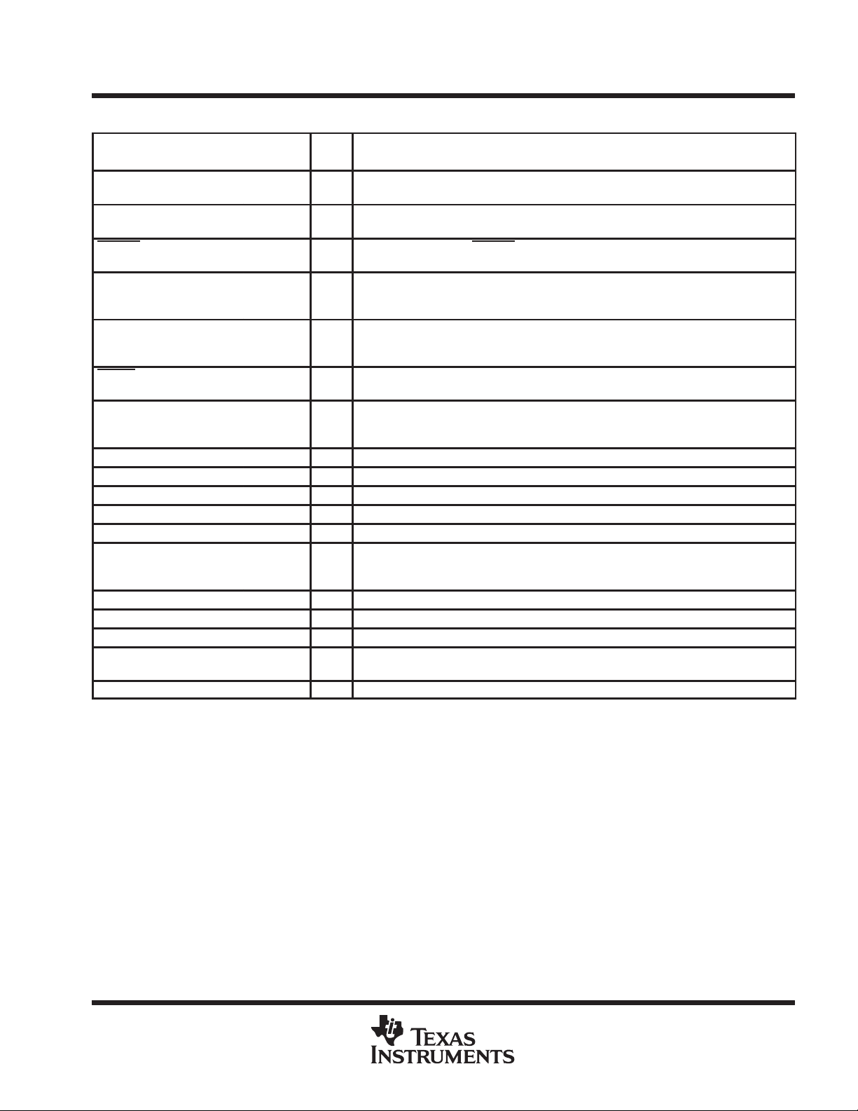
I/O
DESCRIPTION
3.3 V INTEGRATED G.LITE ANALOG FRONT END
SLAS207A – JUNE 1999 – REVISED NOVEMBER 1999
Terminal Functions
TERMINAL
NAME NO.
AMP1INP– AMP4INP 11,2,66,59 I Auxiliary amplifier 1–4 positive input
AMP1INM– AMP4INM 10,3,65,60 I Auxiliary amplifier 1–4 negative input
AMP1OUTP– AMP2OUTP 9,4 O Auxiliary amplifier 1–2 positive output. Outputs are self-biased to AVDD_TX/2.
AMP3OUTP– AMP4OUTP 64, 61 O Auxiliary amplifier 3–4 positive output. Outputs are self-biased to AVDD_RX/2.
AMP1OUTM– AMP2OUTM 12,1 O Auxiliary amplifier 1–2 negative output. Outputs are self-biased to AVDD_TX/2.
AMP3OUTM– AMP4OUTM 67,62 O Auxiliary amplifier 3–4 negative output. Outputs are self-biased to AVDD_RX/2.
AVDD_REF 47 I Analog supply for reference circuit
AVDD_RX 48,68 I RX channel analog supply
AVDD_TX 7 I TX channel analog supply
AVSS_REF 44 I Analog supply return for reference(analog ground)
AVSS_RX 49,69 I RX channel analog supply return (analog ground)
AVSS_TX 8 I TX channel analog supply return (analog ground)
COMPDAC1 16 I TX channel decoupling cap input A. Add 1 µF capacitor to AVDD_TX
COMPDAC2 15 I TX channel decoupling cap input B. Add 1 µF capacitor to AVDD_TX
DGPO 35 O Direct general-purpose output. This pin reflects the last value written to the DGPO bit
DVDD 31,39 I Digital power supply
DVDD_IO 32 I Digital I/O buffer supply
DVDD_RX 51 I RX channel digital supply
DVSS 34,40,41 I Digital ground
DVSS_IO 33 I Digital I/O buffer supply return (digital ground)
DVSS_RX 52,54,55,
56,57
FSX 22 O Serial port frame sync transmit signal
FSR 21 O Serial port frame sync receive signal
GPIO0–GPIO7 23–30 I/O General-purpose I/O
HPF1INP 78 I RX channel stage 1 amplifier positive input. Input signal needs to have AVDD_RX/2
HPF1INM 77 I RX channel stage 1 amplifier negative input. Input signal needs to have AVDD_RX/2
HPF2INP 74 I RX channel stage 2 positive input. Input signal need to have AVDD_RX/2 common mode
HPF2INM 73 I RX channel stage 2 negative input. Input signal need to have AVDD_RX/2 common mode
HPF1OUTP 76 O RX channel stage 1 amplifier positive output. Used to connect external components to obtain
HPF1OUTM 79 O RX channel stage 1 amplifier negative output. Used to connect external components to
HPF2OUTP 72 O RX channel stage 2 positive output. Output signal has AVDD_RX/2 common mode voltage.
HPF2OUTM 75 O RX channel stage 2 negative output. Output signal has AVDD_RX/2 common mode voltage.
MCLKIN/PLLCLKIN 37 I Multiplexed pin based on value of PLLSEL. Selects master clock input, or clock input for PLL
location in the SDR data stream. It is a general-purpose output that does not require a
secondary transfer to control.
I RX channel digital supply return (digital ground)
common mode voltage.
common mode voltage.
voltage.
voltage.
stage 1 HPF.
obtain stage 1 HPF.
mode.
4
POST OFFICE BOX 655303 • DALLAS, TEXAS 75265
I/O
DESCRIPTION
TLFD500PN
3.3 V INTEGRATED G.LITE ANALOG FRONT END
SLAS207A – JUNE 1999 – REVISED NOVEMBER 1999
Terminal Functions (Continued)
TERMINAL
NAME NO.
NC 36,53, 58,
63
PLLSEL 42 I Selects between VCXO mode and DPLL mode. If the pin is tied high PLL mode is selected.
PWRDN 17 I Power-down pin. When PWRDN is pulled low the device goes into power-down mode. The
REFM 45 O Negative reference filter node. This terminal is provided for low-pass filtering of the internal
REFP 46 O Positive reference filter node. This terminal is provided for low-pass filtering of the internal
RESET 38 I Device reset input pin. Initializes all the device’s internal registers to their default values.
RXBANDGAP 43 O RX channel band-gap filter node. This terminal is provided for decoupling of the 1.5-V
RXINP 70 I RX channel stage 3 positive input. The input is self-biased at AVDD_RX/2.
RXINM 71 I RX channel stage 3 negative input. The input is self-biased at AVDD_RX/2.
SCLK 19 O Serial port shift clock (transmit and receive)
SDR 20 I Serial data receive from DSP
SDX 18 O Serial data transmit to DSP
TXBANDGAP 14 O TX channel band-gap filter node. This terminal is provided for decoupling of the 1.5-V
TXOUTP 5 O TX channel positive output
TXOUTM 6 O TX channel negative output
VCXOCNTL 13 O DAC output to control onboard VCXO
VMID_RX 50 I/O Decoupling Vmid for ADC. Add 10 µF (tantalum) and 0.1 µF (ceramic) capacitors to analog
VSS 80 I Substrate. Connect to analog ground.
No connection. Keep floating.
Pin should be tied low for VCXO mode. Cannot be left floating.
default state of this pin is low.
band-gap reference. The optimal ceramic capacitor value is 10 µF (tantalum) and 0.1 µF
(ceramic), connected to analog ground. The nominal dc voltage at this terminal is 0.5 V.
band-gap reference. The optimal ceramic capacitor value is 10 µF (tantalum) 0.1 µF
(ceramic), connected to analog ground. The nominal dc voltage at this terminal is 2.5 V.
The default state of this pin is low.
band-gap reference. The optimal capacitor value is 10 µF (tantalum) and 0.1 µF (ceramic).
This node should not be used as a voltage source.
band-gap reference. The optimal capacitor value is 10 µF (tantalum) and 0.1 µF (ceramic).
This node should not be used as a voltage source.
ground.
detailed description
transmit
The transmit channel is powered by a high performance DAC. The transmit channel update rate is 276 kHz.
The DAC is a 14-bit DAC at 4.416-MHz. This provides 16X oversampling. A band-pass filter limits the output
of the transmitter to a frequency range of 30 kHz to 138 kHz. A differential amplifier drives the output into the
external line driver. The dif ferential amplifier has programmable attenuation for added flexibility. The transmitter
high-pass filter can be bypassed by writing the appropriate bit to the filter bypass control register (BCR).
The output spectrum of the DAC complies with the nonoverlapped power spectrum density (PSD) mask
specified in the ITU draft recommendation G.992.2 for G.Lite.
The TXP AA is a programmable-attenuation amplifier. It provides 0 dB to 24 dB of attenuation in1-dB steps. The
TXP AA is controlled via the P AA control register (PCR). For details about register programming see the register
programming section.
POST OFFICE BOX 655303 • DALLAS, TEXAS 75265
5

TLFD500PN
3.3 V INTEGRATED G.LITE ANALOG FRONT END
SLAS207A – JUNE 1999 – REVISED NOVEMBER 1999
detailed description (continued)
receive
The receive channel consists of a high-pass filter, a programmable gain amplifier, an ADC, and filters. In
addition, it has an equalizer to attain maximum system performance. The input of the receiver is fully differential.
The ADC in the receive channel is a 14-bit converter which samples at 4.416 Msps for 4X oversampling. An
on-chip decimator reduces the sampling frequency to 1.104 MHz. The low pass filtering of the receive channel
limits the converted data to frequencies below 552 kHz.
The high-pass analog filter is used to reject the near-end echo to maximize the dynamic range of the ADC. The
high-pass filter consists of two stages: (1) a second order high-pass filter (HPF1) and, (2) a third order elliptic
high-pass filter (HPF2). Both stages have a cutoff at 180 kHz. The filter is divided into two stages to minimize
the noise from a single stage being amplified throughout. T ogether , the two high-pass filters typically attenuate
the echo power by 30 dB. There is a programmable gain amplifier (PGA) between the two filters for coarse gain
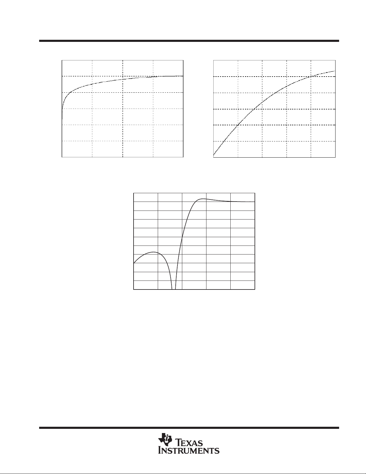
adjustments of 0-dB –12-dB in 3-dB steps. After the high-pass filter stage, the receiver channel has a
0-dB –18-dB PGA that can be adjusted in 6-dB steps. HPF2 and PGAs are integrated in one block. Figure 1(a),
1(b), and 1(c) show the frequency response of HPF1 and HPF2 (with PGAs).
The PGA is followed by a 552-kHz low-pass filter with a programmable 25-dB/MHz slope (5-dB/MHz step)
equalizer incorporated. After the equalizer, there is a fine-gain adjustment PGA of 0-dB to 9-dB in 0.25-dB steps.
All the RX PGAs are controlled via the PGA control registers (PCR–RX1 and PCR–RX2). See the register
programming section for details about register programming.
6
POST OFFICE BOX 655303 • DALLAS, TEXAS 75265
detailed description (continued)
TLFD500PN
3.3 V INTEGRATED G.LITE ANALOG FRONT END
SLAS207A – JUNE 1999 – REVISED NOVEMBER 1999
50
0
–50
–100
Gain – dB
–150
–200
–250
0 0.5 1
f – Frequency – Hz
(a) RX-Stage HPF1 Frequency Response (0 to 200 kHz)
0
–
3
–
6
–
9
–12
dB
–15
–18
–21
–24
–27
1.5 2
× 10
2
0
–2
–4
Gain – dB
–6
–8
–10
5
1 1.2 1.4
f – Frequency – Hz
(b) RX-Stage HPF1 Frequency Response (100 kHz to 200 kHz)
1.6 1.8 2
5
× 10
38.6 90.6 142.
6
(c) RX-Stage HPF2 Frequency Response (PGA1 = PGA2 = 0 dB)
kHz
194.
6
246.
6
298.
6
Figure 1. RX Stage HPF1 and HPF2 Frequency Response
clock control – VCXO mode
The VCXODAC uses a 12-bit, 2s complement number to control a 0-V to 3-V analog output. The two 8-bit
registers, VCR-M and VCR-L, are used to generate the 12-bit control code (2s complement). This implies the
use of 16 bits to obtain a 12-bit number.
VCR-M register occupy the most significant 8 bits in the 12-bit number and the lower 4 bits of the VCR-L register
(VCR-L[3:0] ) are used for the low 4 bits of the 12-bit number. The 12-bit code is updated every time either
register is updated. VCR-L[7:4] must always be zero.
POST OFFICE BOX 655303 • DALLAS, TEXAS 75265
7
TLFD500PN
3.3 V INTEGRATED G.LITE ANALOG FRONT END
SLAS207A – JUNE 1999 – REVISED NOVEMBER 1999
clock control – DPLL mode
As an alternative to the VCXODAC and VCXO, an off-chip crystal oscillator (XO) followed by an on-chip digital
PLL are also implemented. Refer to Figure 7 for an internal function block diagram. The input clock (35.328
MHz) goes to a programmable frequency divider to generate sampling clock for the ADC and DAC converters.
By changing the divide ratio, the phase of the sampling clock can be adjusted. Setting PLLSEL (pin 42) high
will enable the DPLL mode. Refer to DPLL section for detail.
clock generation
The clock generation block creates the necessary internal and external clocks needed by the device. All the
clocks generated are produced from the CLKIN signal.
The following are recommended operational parameters for the external VCXO:
3.3-V supply, 35.328 MHz ±50 PPM center frequency , and input control voltage range of 0 V–3 V.
The recommended duty cycle is 50/50.
clock generation – SCLK
SCLK is an output and is used for serial data transfer. It runs at 35.328 MHz. Although SCLK and MCLK run
at the same speed, there is no fixed phase relationship between them.
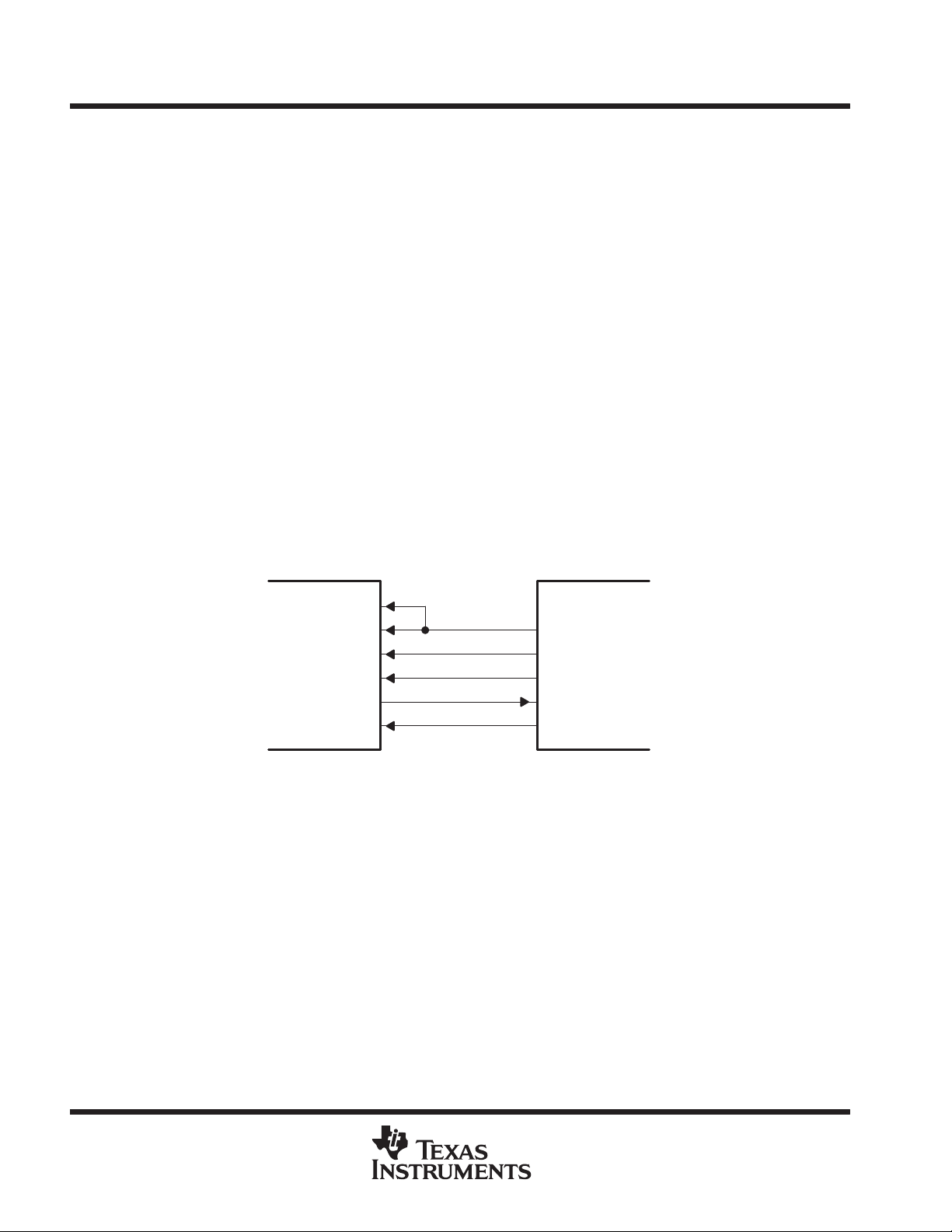
serial interface
The serial interface on the TLFD500PN connects directly to TI’s C54x or C6x families of DSPs. The interface
operates at 35.328 MHz. The serial port consists of five signals: SCLK, FSX, FSR, SDX, and SDR. A typical
connection diagram is shown in Figure 2.
DSP
CLKR
CLKX
FSX
FSR
DX
DR
TLFD500PN
SCLK
FSR
FSX
SDR
SDX
Figure 2. Typical Serial Port Connection
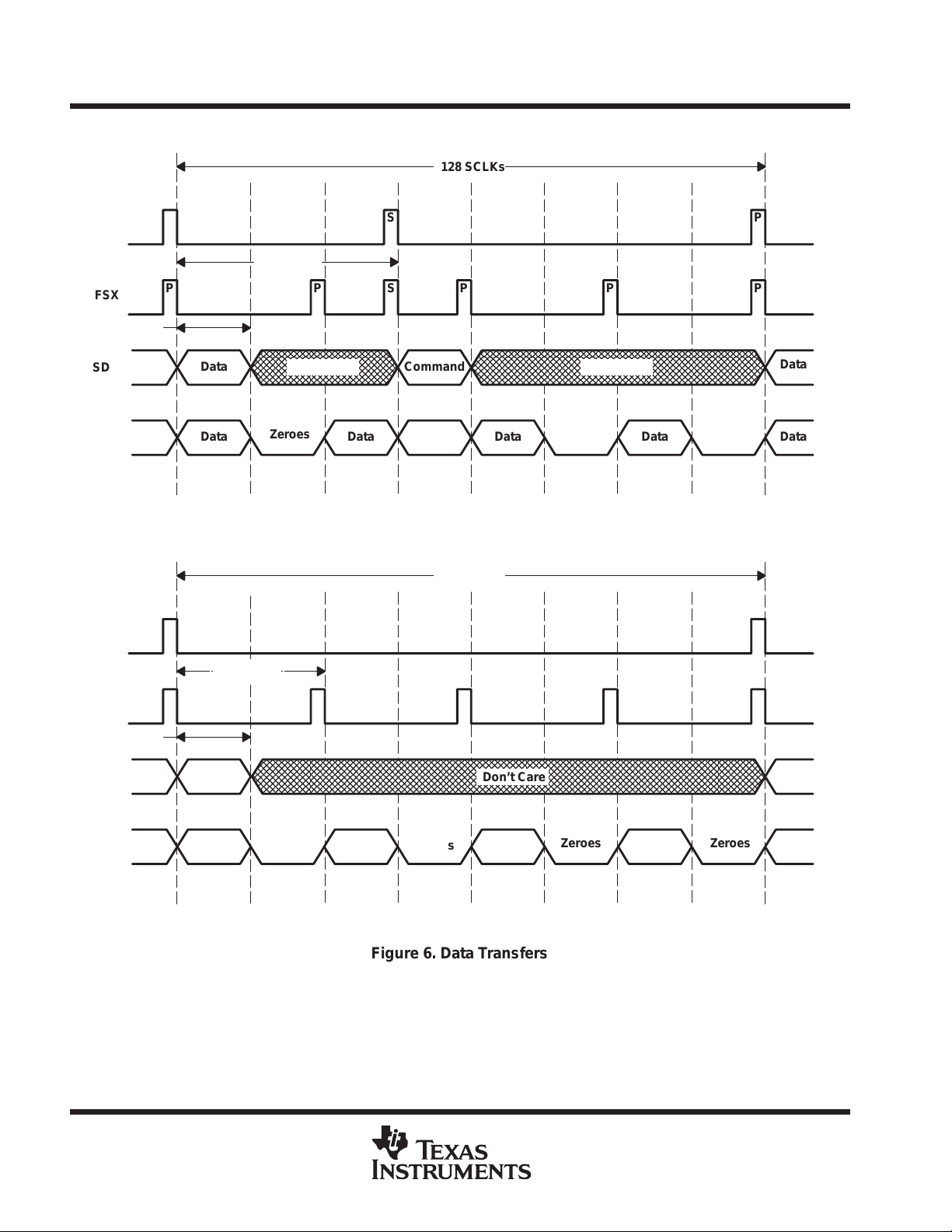
The serial port utilizes a primary/secondary scheme to transfer conversion data and control register data. A
primary transfer scheme, used to transfer conversion data, occurs every conversion period. A secondary
transfer scheme, used to transfer control data, happens only when requested by the host processor. The host
processor requests a secondary transfer by using the LSB of the SDR data of the primary scheme. A value of
1 indicates a secondary transfer request. Once the secondary request is made and the primary transfer has
been completed, secondary frame sync pulse (FSX/FSR) are transmitted to the host processor to indicate the
beginning of the secondary transfer. The secondary FSX signal arrives 16 SCLKs after the primary FSX, and
thus 48 SCLKs after the host processor request. This is because the span between FSX pulses for primary
transfers is always 32 SCLKs. Each bit is read/written at the rising edge of the SCLK clock. Data bit mappings
and example data transfers are shown in Table 1.
8
POST OFFICE BOX 655303 • DALLAS, TEXAS 75265
TLFD500PN
3.3 V INTEGRATED G.LITE ANALOG FRONT END
SLAS207A – JUNE 1999 – REVISED NOVEMBER 1999
detailed description (continued)
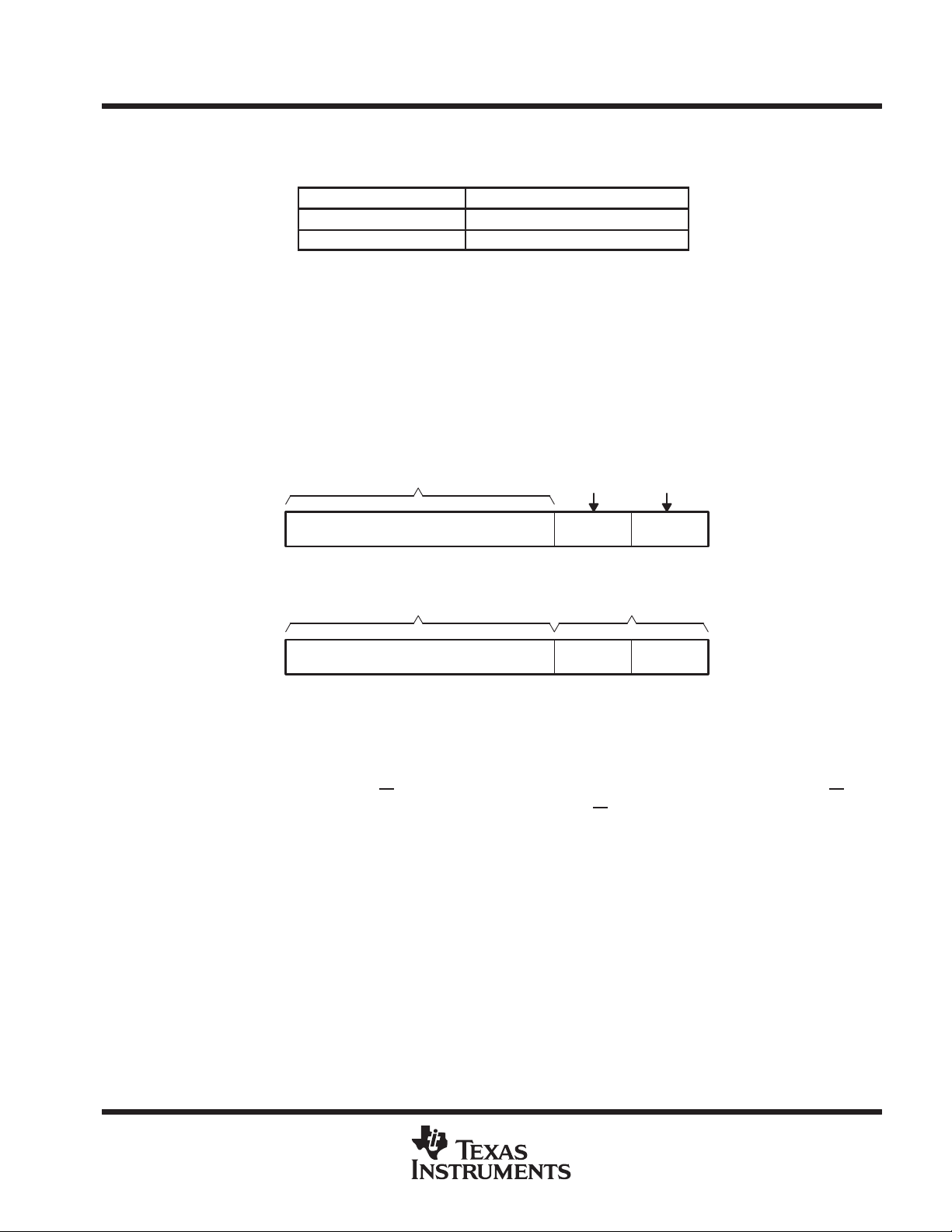
Table 1. SDR LSB Control Function
CONTROL BIT D0 CONTROL BIT FUNCTION
0 No secondary transfer requested
1 Secondary transfer requested
primary transfer data mapping
The data bit mapping of a primary transfer is shown in Figure 3. Bits D2–D15 of the SDR data stream are DAC
data. D1 is the control bit for the DGPO pin. The value written to this bit is reflected on the DGPO pin. See the
timing diagram in Figures 5 and 6 for detailed timing information. D0 is the secondary transfer request bit. When
a 1 is written to this bit, the host is requesting a secondary data transfer.
In the SDX data stream, D2–D15 contain the ADC conversion data. D0 and D1 can be set to reflect the values
of GPIO1 and GPIO2. To set D0 and D1 to reflect the GPIO values, the proper bit in the MCR register needs
to be set.
Secondary
Transfer
Data to CODEC
DGPO Bit
Request
SDR
SDX
GPIOx Status if Configured as
Input. Zero if GPIOx Configured
Data from CODEC
D15 – D2
D1 D0D15 – D2
as output or if Masked Off
GPIO1 GPIO0
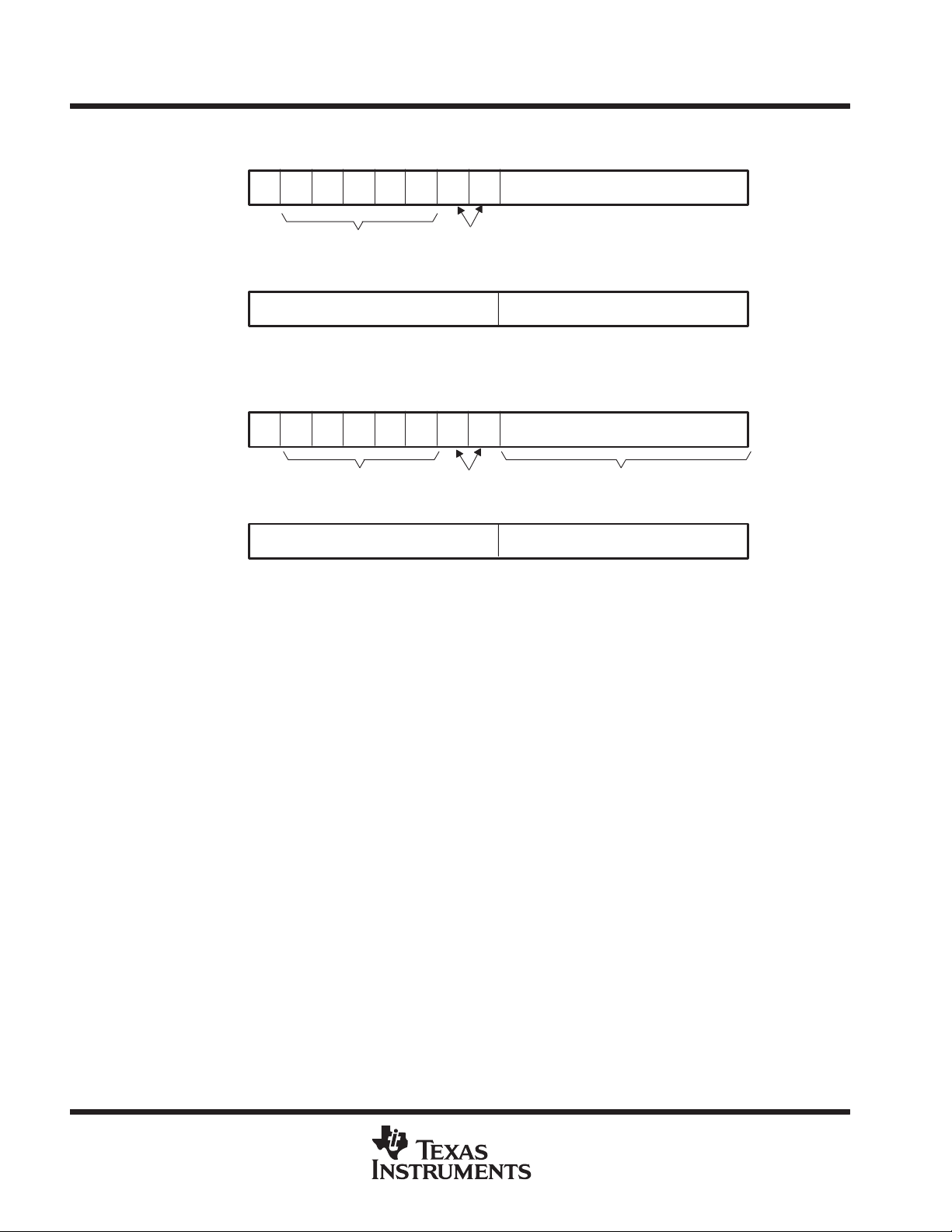
Figure 3. Primary Transfer Data Bit Mapping
secondary transfer data mapping
Secondary serial communication is used to configure the device. The data bit mapping for a secondary transfer
is shown in Figure 4. Bits D10–D14 of the SDR data from the host contain the address of the control register
involved in the transfer. D15 is a R/W bit. To read out the control register by the host processor, bit R/W must
be set to 1. T o write to the control register by the host processor, bit R/W must be set to 0. During a read operation,
bits D0–D7 are don’t care. For a write operation, bits D0–D7 contain the data for the register addressed by
D10–D14. The eight bits of SDX always reflect the status of GPI00–7.
If the secondary transfer is a read operation, the contents of the control register addressed by D10–D14 of the
SDR data are reflected in bits D0–D7 of the SDX data stream. If the secondary transfer is a write operation, bits
D0–D7 on SDX will be all zeroes.
POST OFFICE BOX 655303 • DALLAS, TEXAS 75265
9
TLFD500PN
3.3 V INTEGRATED G.LITE ANALOG FRONT END
SLAS207A – JUNE 1999 – REVISED NOVEMBER 1999
secondary transfer data mapping (continued)
D9 D0
A0
SDR (Read)
SDX (Read)
D15
A4 A3 A2 A1
1
Register Address Don’t Care
D15 D0D8 D7
GPIO0 – 7 Status
Read Cycle (Codec Register Data Read by DSP)
D8 D7
Don’t Care
Register Data
SDR (Write)
SDX (Write)
D9 D8 D7
0
A4 A3 A2
Register Address
D15 D0D8 D7
GPIO0 – 7 Status
A1 A0
Don’t Care
Write Cycle (DSP Data Write to Codec Register)
Data to the Register
All 0
D0
Figure 4. Secondary Transfer Data Bit Mapping
example data transfers
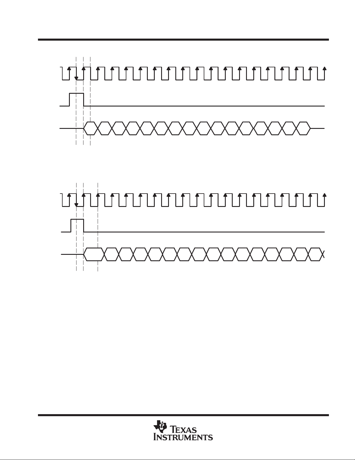
Figures 5(a) and 5(b) show the timing relationship for SCLK, FSX, SDX, FSR, and SDR in a primary
communication. The timing sequence for this operation is as follows:
1. FS is set high and remains high during one SCLK period, then returns to low.
2. A 16-bit word is transmitted from the ADC (SDX), and a 16-bit word is received for DAC conversion (SDR).
Figure 6(a) and 6(b) shows the timing relationship with secondary request.
10
POST OFFICE BOX 655303 • DALLAS, TEXAS 75265
detailed description (continued)
SCLK
(Output)
FSX
(output)
TLFD500PN
3.3 V INTEGRATED G.LITE ANALOG FRONT END
SLAS207A – JUNE 1999 – REVISED NOVEMBER 1999
SDX
(Output)
SCLK
(Output)
FSR
(output)
SDR
(Input)
D15 D14 D13 D12 D11 D10 D9 D8 D7 D6 D5 D4 D3 D2 D1 D0
t1 t2 t3
t1 t2 t3
t1: DSP detects FSX
t2: TLFD500PN sends data
t3: DSP latches data
D15
D14 D13 D12 D11 D10 D9 D8 D7 D6 D5 D4 D3 D2 D1 D0
t1: DSP detects FSR
t2: DSP sends data
t3: TLFD500PN latches data
(a) TLFD500PN to DSP
(b) DSP to TLFD500PN
NOTE: TI DSP requires 10 ns after the positive edge of the SCLK to give the SDR data. This plus the board delay, output buffer (for SCLK) and
input buffer delay (for SDR) to around 17 ns. As a consequence the SDR data can not be latched at the negative edge of SCLK.
Figure 5. Data Transfers
POST OFFICE BOX 655303 • DALLAS, TEXAS 75265
11
TLFD500PN
3.3 V INTEGRATED G.LITE ANALOG FRONT END
SLAS207A – JUNE 1999 – REVISED NOVEMBER 1999
detailed description (continued)
128 SCLKs
FSR
FSX
16 SCLKs
SDR
SDX
FSR
P
48 SCLKs
Data Command
Data Data Data Data Data
P
Don’t Care Don’t Care
Zeroes
S
Status
(a) With Secondary Request
128 SCLKs
Zeroes Zeroes
P
PPPPPS
Data
P
FSX
16 SCLKs
SDR
SDX
32 SCLKs
PPPPP
Data
Data Data Data Data Data
Zeroes
Zeroes
(b) Without Secondary Request
Don’t Care
Zeroes Zeroes
Data
Figure 6. Data Transfers
12
POST OFFICE BOX 655303 • DALLAS, TEXAS 75265

TLFD500PN
3.3 V INTEGRATED G.LITE ANALOG FRONT END
SLAS207A – JUNE 1999 – REVISED NOVEMBER 1999
detailed description (continued)
general purpose I/O port (GPIO)
The general-purpose I/O port provides eight input/output pins and one output-only pin for control of external
circuitry , or for reading the status of external devices. The eight input/output pins are labeled GPIO0 –GPIO7.
The output-only pin is labeled DGPO (direct general-purpose output). This pin is labeled as direct because a
secondary transfer is not required to write to this pin.
The GPIO pins are controlled and read in the GPR-D register. The GPR-C register is used to configure the GPIO
pins as input or output pins. The default reset condition is 1 1111111b, indicating that all are configured as inputs.
For further details on register programming see the register programming section. The DGPO pin does not need
configuring and is controlled by the D1 bit in the SDR data stream (that is, from the DSP to the TLFD500PN)
during primary data transfers. In addition, a secondary transfer is not required to read GPIO0 and GPIO1 when
they are configured as inputs. Their values can be mapped into the lower two bits of the SDX data stream (that
is, from TLFD500PN to DSP) during primary data transfers. To map the values of GPIO0 and GPIO1 into the
lower two bits of the SDX ADC data stream, set the appropriate bit in the MCR register.
For more flexibility, the values of GPIO0 – GPIO7 are mapped into the upper eight data bits of the SDX data
stream on secondary data transfers. This allows the host processor to read the values of the GPIO pins and
the contents of another control register during the same secondary data transfer. When a GPIO pin is being
configured as an output, its corresponding status bit in the SDX data stream will be the last value written to the
output pin.
Each output is capable of driving 2 mA.
reference system
The integrated reference provides voltage and current to the internal analog blocks. It is also brought out to
external pins for noise decoupling. They should not be used as dc voltage source.
When the internal reference is being used by the device, the device may be powered down by writing the
appropriate reference control bit in the main control register (MCR) to achieve power savings during periods
of device inactivity.
auxiliary amplifiers
Four auxiliary high-performance operational amplifiers on the chip allow for additional onboard filtering and
amplification with minimal component count. Each op-amp has differential inputs and outputs, with 2 input pins
and 2 output pins. Each op-amp can be enabled by register programming.
The typical specifications for the operational amplifiers are as follows:
DC Gain: 126 dB
Bandwidth: 116 MHz
PSRR: 100 dB at dc, 70 dB at 1 MHz, and 40 dB at 4 MHz
Output common-mode: AVDD_RX/2 (auxiliary amplifier 3,4) or AVDD_TX/2 (auxiliary amplifier 1,2)
Input interface: AC coupled
device power-up sequence
All digital and analog supplies must be properly biased. All supply pins are mandatory . The power supply can
not be switched, even when the codec has been powered down or parts of the codec are in power-down mode.
Reset must be held at least 20 µs after power up. To reset the reference circuit and registers requires 100 ms.
When the chip is woken up from hardware power-down mode, it takes100 ms to reset the reference circuit
before the chip works in normal mode. When the chip is woken up from software power-down mode, only 20
µs is needed before valid data comes out (reference must be kept on). Register values will not change in either
wake-up operation.
POST OFFICE BOX 655303 • DALLAS, TEXAS 75265
13

TLFD500PN
NAME
3.3 V INTEGRATED G.LITE ANALOG FRONT END
SLAS207A – JUNE 1999 – REVISED NOVEMBER 1999
detailed description (continued)
register programming
The codec registers are listed in Table 2, with each bit of each register defined. All registers are 8-bit wide.
NOTE:
Bits not defined in the table are reserved for future use. During a read, the reserved bit read value
is not guaranteed. During a write, only zeroes can be written to reserved bits.
Table 2. Codec Registers
REGISTER
ADDRESS
A4 A3 A2 A1 A0
BCR 00001 R/W D0: Power-down RX HP filter 1
PCR-RX1 00010 R/W D[5:0] = RXPGA3[5:0]; Fine gain, 0 to 9 dB, 0.25-dB steps
PCR-RX2 00011 R/W D[2:0] = RXPGA1[2:0]; 0 to 12dB, 3-dB steps
PCR-TX 00100 R/W D[4:0] = TX PAA[4:0]; 0 to –24dB, –1-dB steps
EQR 00101 R/W D[2:0] = EQ[2:0] 0 to 25 dB, 5 dB/MHz steps; D[6:4] = EQ_PGA[2:0] 0 to 6 dB, 1 dB
VCR-M 00110 R/W D[7:0] = VCXO DAC control Bit[11:4].
VCR-L 00111 R/W D[3:0] = VCXO DAC control Bit[3:0]. D[7:4] must always be zero.
GPR-C 01000 R/W D[7:0] = GPIO1 I/O control (0 = output, 1 = input)
GPR-D 01001 R/W D[7:0] = GPIO data register
Reserved 01010 R/W For future use. Read or write of register not allowed.
AUXR 0101 1 R/W D0: Enable auxiliary amplifier 2
NCO_DEF 01100 R/W D[7:0] = Default NCO divide number
NCO_DIV_DELAY 01 101 R/W D[7:0] = Number of samples, from current secondary transfer, after which effect of delta
NCO_DELTA 01110 R/W D[7:4] = Delta from default for first sample of data frame (–8 through 7)
MCR 01111 R/W D0: S/W Power-down main reference
MODE FUNCTION
D1: Power-down RX HP filter 2
D2: Bypass TX digital HP filter
D3: Echo mode: Echo SDR data back to SDX
D4: Reserved
D5: Reserved
D6: Reserved
D[4:3] = RXPGA2[1:0]; 0 to 18 dB, 6-dB steps
steps
D1: Enable auxiliary amplifier 1
D2: Enable auxiliary amplifier 3
D3: Enable auxiliary amplifier 4
will occur.
D[3:0] = Number of times NCO divider remains changed from default before being set
back to default (0 through 15)
D1: S/W Power-down TX channel with reference still on
D2: S/W Power-down RX channel with reference still on
D3: S/W Power-down VCXO with reference still on
D4: S/W Reset
D5: Analog loop back (refer to block diagram)
D6: Digital loop back (refer to block diagram)
D7: Enable GPIO 1 and 2 to show in SDX primary data
14
POST OFFICE BOX 655303 • DALLAS, TEXAS 75265

ECHO
TXHPEN
RXHP2PD
RXHP1PD
TLFD500PN
3.3 V INTEGRATED G.LITE ANALOG FRONT END
SLAS207A – JUNE 1999 – REVISED NOVEMBER 1999
BCR – bypass control register
Address: 00001b Contents at reset: 00000000b
D7
Reserved Reserved Reserved Reserved ECHO TXHPEN RXHP2PD RXHP1PD
D7 D6 D5 D4 D3 D2 D1 D0 REG. VALUE BIT NAME DESCRIPTION
R – – – – – – – – Reserved Bit reserved for future use
– R – – – – – – – Reserved Bit reserved for future use
– – R – – – – – – Reserved Bit reserved for future use
– – – R – – – – – Reserved Bit reserved for future use
– – – – 0 – – – –
– – – – 1 – – – 0x08
– – – – – 0 – – –
– – – – – 1 – – 0x04
– – – – – – 0 – –
– – – – – – 1 – 0x02
– – – – – – – 0 –
– – – – – – – 1 0x01
NOTE 1: ECHO mode allows for a quick verification of the serial interface operation. It sends back the data from input data buffer to the output
data buffer and does not exercise the RX or TX channel.
D6 D5 D4 D3 D2 D1 D0
Table 3. EQR Bit Definition
Do not echo SDR data on SDX
Echo SDR data on SDX (see Note 1)
Enable TX HP Filter
Bypass TX HP Filter
Power up RX HP Filter 2
Power down RX HP Filter 2
Power up RX HP Filter 1
Power down RX HP Filter 1
POST OFFICE BOX 655303 • DALLAS, TEXAS 75265
15

TLFD500PN
3.3 V INTEGRATED G.LITE ANALOG FRONT END
SLAS207A – JUNE 1999 – REVISED NOVEMBER 1999
PCR-RX1 – programmable gain control register 1 for RX channel PGA3
Address: 00010b Contents at reset: 00000000b
D7
Reserved Reserved RXPGA3[5] RXPGA3[4] RXPGA3[3] RXPGA3[2] RXPGA3[1] RXPGA3[0]
D7 D6 D5 D4 D3 D2 D1 D0 HEX VALUE BIT NAME DESCRIPTION
R – – – – – – – – Reserved Bit reserved for future use
– R – – – – – – – Reserved Bit reserved for future use
– 0 0 0 0 0 0 0x00 RXPGA3[5:0] 0dB
– 0 0 0 0 0 1 0x01 0.25dB
– – 0 0 0 0 1 0 0x02 0.50dB
– – 0 0 0 0 1 1 0x03 0.75dB
– – 0 0 0 1 0 0 0x04 1.00dB
– – 0 0 0 1 0 1 0x05 1.25dB
– – 0 0 0 1 1 0 0x06 1.50dB
– – 0 0 0 1 1 1 0x07 1.75dB
– – 0 0 1 0 0 0 0x08 2.00dB
– – 0 0 1 0 0 1 0x09 2.25dB
– – 0 0 1 0 1 0 0x0A 2.50dB
– – 0 0 1 0 1 1 0x0B 2.75dB
– – 0 0 1 1 0 0 0x0C 3.00dB
– – 0 0 1 1 0 1 0x0D 3.25dB
– – 0 0 1 1 1 0 0x0E 3.50dB
– – 0 0 1 1 1 1 0x0F 3.75dB
– – 0 1 0 0 0 0 0x10 4.00dB
– – 0 1 0 0 0 1 0x11 4.25dB
– – 0 1 0 0 1 0 0x12 4.50dB
– – 0 1 0 0 1 1 0x13 4.75dB
– – 0 1 0 1 0 0 0x14 5.00dB
– – 0 1 0 1 0 1 0x15 5.25dB
– – 0 1 0 1 1 0 0x16 5.50dB
– – 0 1 0 1 1 1 0x17 5.75dB
– – 0 1 1 0 0 0 0x18 6.00dB
– – 0 1 1 0 0 1 0x19 6.25dB
– – 0 1 1 0 1 0 0x1A 6.50dB
– – 0 1 1 0 1 1 0x1B 6.75dB
– – 0 1 1 1 0 0 0x1C 7.00dB
– – 0 1 1 1 0 1 0x1D 7.25dB
– – 0 1 1 1 1 0 0x1E 7.50dB
– – 0 1 1 1 1 1 0x1F 7.75dB
– – 1 0 0 0 0 0 0x20 8.00dB
– – 1 0 0 0 1 1 0x21 8.25dB
– – 1 0 0 1 0 0 0x22 8.50dB
D6 D5 D4 D3 D2 D1 D0
T able 4. PCR-RX1 Gain
16
POST OFFICE BOX 655303 • DALLAS, TEXAS 75265

3.3 V INTEGRATED G.LITE ANALOG FRONT END
SLAS207A – JUNE 1999 – REVISED NOVEMBER 1999
Table 4. PCR-RX1 Gain (Continued)
D7 D6 D5 D4 D3 D2 D1 D0 HEX VALUE BIT NAME DESCRIPTION
– – 1 0 0 0 1 1 0x23 RXPGA3[5:0] 8.75dB
– – 1 0 0 1 0 0 0x24 9.00dB
– – 1 0 0 1 0 1 0x25 INVALID
– – 1 0 0 1 1 0 0x26 INVALID
– – 1 0 0 1 1 1 0x27 INVALID
– – 1 0 1 0 0 0 0x28 INVALID
– – 1 0 1 0 0 1 0x29 INVALID
– – 1 0 1 0 1 0 0x2A INVALID
– – 1 0 1 0 1 1 0x2B INVALID
– – 1 0 1 1 0 0 0x2C INVALID
– – 1 0 1 1 0 1 0x2D INVALID
– – 1 0 1 1 1 0 0x2E INVALID
– – 1 0 1 1 1 1 0x2F INVALID
– – 1 1 0 0 0 0 0x30 INVALID
– – 1 1 0 0 0 1 0x31 INVALID
– – 1 1 0 0 1 0 0x32 INVALID
– – 1 1 0 0 1 1 0x33 INVALID
– – 1 1 0 1 0 0 0x34 INVALID
– – 1 1 0 1 0 1 0x35 INVALID
– – 1 1 0 1 1 0 0x36 INVALID
– – 1 1 0 1 1 1 0x37 INVALID
– – 1 1 1 0 0 0 0x38 INVALID
– – 1 1 1 0 0 1 0x39 INVALID
– – 1 1 1 0 1 0 0x3A INVALID
– – 1 1 1 0 1 1 0x3B INVALID
– – 1 1 1 1 0 0 0x3C INVALID
– – 1 1 1 1 0 1 0x3D INVALID
– – 1 1 1 1 1 0 0x3E INVALID
– – 1 1 1 1 1 1 0x3F INVALID
NOTE 2: The formula to convert bit value to RXPGA3 gain in dB is
RXPGA3 gain (in dB) = RXPGA3[5:0] (in decimal) x 0.25dB
Similarly one can compute the RXPGA3 [5:0] bit combination needed, given the gain in dB.
CAUTION:
Performance of the codec for invalid combination of bits is not guaranteed and such
combinations should not be used. The user should make no assumption that the code bits
will saturate to a maximum or minimum value or wrap around to a valid combination.
TLFD500PN
POST OFFICE BOX 655303 • DALLAS, TEXAS 75265
17

TLFD500PN
3.3 V INTEGRATED G.LITE ANALOG FRONT END
SLAS207A – JUNE 1999 – REVISED NOVEMBER 1999
PCR-RX2 – programmable gain control register 2 for RX channel PGA1 and PGA2
Address: 00011b Contents at reset: 00000000b
D7
Reserved Reserved Reserved RXPGA2[1] RXPGA2[0] RXPGA1[2] RXPGA1[1] RXPGA1[0]
D7 D6 D5 D4 D3 D2 D1 D0 HEX VALUE BIT NAME DESCRIPTION
R – – – – – – – – Reserved Bit reserved for future use
– R – – – – – – – Reserved Bit reserved for future use
– – R – – – – – – Reserved Bit reserved for future use
– – – 0 0 – – – 0x00 RXPGA2[1:0] 0dB
– – – 0 1 – – – 0x08 6dB
– – – 1 0 – – – 0x10 12dB
– – – 1 1 – – – 0x18 18dB
– – – – – 0 0 0 0x00 RXPGA1[2:0] 0dB
– – – – – 0 0 1 0x01 3dB
– – – – – 0 1 0 0x02 6dB
– – – – – 0 1 1 0x03 9dB
– – – – – 1 0 0 0x04 12dB
– – – – – 1 0 1 0x05 INVALID
– – – – – 1 1 0 0x06 INVALID
– – – – – 1 1 1 0x07 INVALID
NOTES: 3. The formula to convert bit value to RXPGA2 gain in dB is
RXPGA2 gain (in dB) = RXPGA2[1:0] (in decimal) x 6dB
Similarly the needed RXPGA2[1:0] bit combination can be computed, given the gain in dB.
4. The formula to convert bit value to RXPGA1 gain in dB is
RXPGA1 gain (in dB) = RXPGA1[2:0] (in decimal) x 3dB
Similarly the needed RXPGA1[2:0] bit combination can be computed, given the gain in dB.
Performance of the codec for invalid combination of bits is not guaranteed and such
combinations should not be used. The user should make no assumption that the code bits
will saturate to a maximum or minimum value or wrap around to a valid combination.
D6 D5 D4 D3 D2 D1 D0
T able 5. PCR-RX2 Gain
CAUTION:
PCR-TX – programmable attenuation control register for TX channel
Address: 00100b Contents at reset: 00000000b
D7
Reserved Reserved Reserved TXPAA[4] TXPAA[3] TXPAA[2] TXPAA[1] TXPAA[0]
18
D6 D5 D4 D3 D2 D1 D0
POST OFFICE BOX 655303 • DALLAS, TEXAS 75265

TLFD500PN
3.3 V INTEGRATED G.LITE ANALOG FRONT END
SLAS207A – JUNE 1999 – REVISED NOVEMBER 1999
PCR-TX – programmable attenuation control register for TX channel (continued)
Table 6. PCR-TX Attenuation
D7 D6 D5 D4 D3 D2 D1 D0 HEX VALUE BIT NAME DESCRIPTION
R – – – – – – – – Reserved Bit reserved for future use
– R – – – – – – – Reserved Bit reserved for future use
– – R – – – – – – Reserved Bit reserved for future use
– – – 0 0 0 0 0 0x00 TXPAA[4:0] –0 dB
– – – 0 0 0 0 1 0x01 –1 dB
– – – 0 0 0 1 0 0x02 –2 dB
– – – 0 0 0 1 1 0x03 –3 dB
– – – 0 0 1 0 0 0x04 –4 dB
– – – 0 0 1 0 1 0x05 –5 dB
– – – 0 0 1 1 0 0x06 –6 dB
– – – 0 0 1 1 1 0x07 –7 dB
– – – 0 1 0 0 0 0x08 –8 dB
– – – 0 1 0 0 1 0x09 –9 dB
– – – 0 1 0 1 0 0x0A –10 dB
– – – 0 1 0 1 1 0x0B –11 dB
– – – 0 1 1 0 0 0x0C –12 dB
– – – 0 1 1 0 1 0x0D –13 dB
– – – 0 1 1 1 0 0x0E –14 dB
– – – 0 1 1 1 1 0x0F –15 dB
– – – 1 0 0 0 0 0x10 –16 dB
– – – 1 0 0 0 1 0x11 –17 dB
– – – 1 0 0 1 0 0x12 –18 dB
– – – 1 0 0 1 1 0x13 –19 dB
– – – 1 0 1 0 0 0x14 –20 dB
– – – 1 0 1 0 1 0x15 –21 dB
– – – 1 0 1 1 0 0x16 –22 dB
– – – 1 0 1 1 1 0x17 –23 dB
– – – 1 1 0 0 0 0x18 –24 dB
– – – 1 1 0 0 1 0x19 INVALID
– – – 1 1 0 1 0 0x1A INVALID
– – – 1 1 0 1 1 0x1B INVALID
– – – 1 1 1 0 0 0x1C INVALID
– – – 1 1 1 0 1 0x1D INVALID
– – – 1 1 1 1 0 0x1E INVALID
– – – 1 1 1 1 1 0x1F INVALID
NOTE 5: The formula to convert bit value to TXP AA attenuation in dB is
TXPAA attenuation (in dB) = TXPAA[4:0] (in decimal) x (–1)dB
Similarly one can compute the TXPAA[4:0] bit combination needed, given the attenuation in dB.
CAUTION:
Performance of the codec for invalid combination of bits is not guaranteed and such
combinations should not be used. The user should make no assumption that the code bits
will saturate to a maximum or minimum value or wrap around to a valid combination.
POST OFFICE BOX 655303 • DALLAS, TEXAS 75265
19

TLFD500PN
3.3 V INTEGRATED G.LITE ANALOG FRONT END
SLAS207A – JUNE 1999 – REVISED NOVEMBER 1999
EQR – equalizer slope and gain control register
Address: 00101b Contents at reset: 00000000b
D7
Reserved EQPGA[2] EQPGA[1] EQPGA[0] Reserved EQ[2] EQ[1] EQ[0]
D7 D6 D5 D4 D3 D2 D1 D0 HEX VALUE BIT NAME DESCRIPTION
R – – – – – – – – Reserved Bit reserved for future use
– 0 0 0 – – – – 0x00 EQPGA[2:0] 0dB
– 0 0 1 – – – – 0x10 1dB
– 0 1 0 – – – – 0x20 2dB
– 0 1 1 – – – – 0x30 3dB
– 1 0 0 – – – – 0x40 4dB
– 1 0 1 – – – – 0x50 5dB
– 1 1 0 – – – – 0x60 6dB
– 1 1 1 – – – – 0x70 INVALID
– – – – R – – – – Reserved Bit reserved for future use
– – – – – 0 0 0 0x00 EQ[2:0] 0dB slope
– – – – – 0 0 1 0x01 5dB slope
– – – – – 0 1 0 0x02 10dB slope
– – – – – 0 1 1 0x03 15dB slope
– – – – – 1 0 0 0x04 20dB slope
– – – – – 1 0 1 0x05 25dB slope
– – – – – 1 1 0 0x06 INVALID
– – – – – 1 1 1 0x07 INVALID
NOTES: 6. The formula to convert bit value to EQPGA gain in dB is
EQPGA gain (in dB) = EQPGA[2:0] (in decimal) x 1 dB
Similarly one can compute the EQPGA[2:0] bit combination needed, given the gain in dB.
7. The formula to convert bit value to EQ slope in dB is
EQ slope (in dB/MHz) =EQ[2:0] (in decimal) x 5 dB/MHz
Similarly one can compute the EQ[2:0] bit combination needed, given the slope in dB/MHz.
Performance of the codec for invalid combination of bits is not guaranteed and such
combinations should not be used. The user should make no assumption that the code bits
will saturate to a maximum or minimum value or wrap around to a valid combination.
D6 D5 D4 D3 D2 D1 D0
Table 7. EQR Slope and Gain
CAUTION:
20
POST OFFICE BOX 655303 • DALLAS, TEXAS 75265

VCR-M – VCXO DAC control register MSB
Address: 00110b Contents at reset: 00000000b
D7
VCR–M[7] VCR–M[6] VCR–M[5] VCR–M[4] VCR–M[3] VCR–M[2] VCR–M[1] VCR–M[0]
VCR-L – VCXO DAC control register LSB
Address: 00111b Contents at reset: 00000000b
D7
0 0 0 0 VCR–L[3] VCR–L[2] VCR–L[1] VCR–L[0]
Table 8 shows some representative analog outputs.
VCR–M[7:0] * 24 + VCR–L[3:0] 0x800 0 V Min scale
Where step–size, ∆ = (3/4095) V.
D6 D5 D4 D3 D2 D1 D0
D6 D5 D4 D3 D2 D1 D0
Table 8. Representative Analog Outputs
OPERATION HEX RESULT ANALOG OUTPUT COMMENTS
TLFD500PN
3.3 V INTEGRATED G.LITE ANALOG FRONT END
SLAS207A – JUNE 1999 – REVISED NOVEMBER 1999
0x801 ∆V Just above min
… … …
0xFFF 2047∆V Just below mid
0x000 2048∆V Mid scale
0x001 2049∆V Just above mid
… … …
0x7FE 4094∆V Just below max
0x7FF 4095∆V Max scale
For example,if 0xAA7 is desired, VCR-M and VCR-L should be set to 0xAA and 0x07;
if 0x539 is desired, VCR-M and VCR-L should be set to 0x53 and 0x09.
POST OFFICE BOX 655303 • DALLAS, TEXAS 75265
21

TLFD500PN
GPIOC[7]
GPIOC[6]
GPIOC[5]
GPIOC[4]
GPIOC[3]
GPIOC[2]
GPIOC[1]
GPIOC[0]
3.3 V INTEGRATED G.LITE ANALOG FRONT END
SLAS207A – JUNE 1999 – REVISED NOVEMBER 1999
GPR-C – GPIO I/O direction control register
Address: 01000b Contents at reset: 11111111b
D7
GPIOC[7] GPIOC[6] GPIOC[5] GPIOC[4] GPIOC[3] GPIOC[2] GPIOC[1] GPIOC[0]
D7 D6 D5 D4 D3 D2 D1 D0 REG VALUE BIT NAME DESCRIPTION
0 – – – – – – – –
1 – – – – – – – 0x80
– 0 – – – – – – –
– 1 – – – – – – 0x40
– – 0 – – – – – –
– – 1 – – – – – 0x20
– – – 0 – – – – –
– – – 1 – – – – 0x10
– – – – 0 – – – –
– – – – 1 – – – 0x08
– – – – – 0 – – –
– – – – – 1 – – 0x04
– – – – – – 0 – –
– – – – – – 1 – 0x02
– – – – – – – 0 –
– – – – – – – 1 0x01
NOTE 8: A particular GPIOC control bit configures direction for the corresponding GPIOD data bit.
D6 D5 D4 D3 D2 D1 D0
Table 9. GPR-C Direction Control
Configure GPIO 7 pin as output
Configure GPIO 7 pin as input
Configure GPIO 6 pin as output
Configure GPIO 6 pin as input
Configure GPIO 5 pin as output
Configure GPIO 5 pin as input
Configure GPIO 4 pin as output
Configure GPIO 4 pin as input
Configure GPIO 3 pin as output
Configure GPIO 3 pin as input
Configure GPIO 2 pin as output
Configure GPIO 2 pin as input
Configure GPIO 1 pin as output
Configure GPIO 1 pin as input
Configure GPIO 0 pin as output
Configure GPIO 0 pin as input
GPR-D – GPIO data register
Address: 01001b Contents at reset: 00000000b
D7
GPIOD[7] GPIOD[6] GPIOD[5] GPIOD[4] GPIOD[3] GPIOD[2] GPIOD[1] GPIOD[0]
GPIOD[7:0] corresponds to pins GPIO7–GPIO0 respectively.
D6 D5 D4 D3 D2 D1 D0
CAUTION:
22
POST OFFICE BOX 655303 • DALLAS, TEXAS 75265

AMP4EN
AMP3EN
AMP1EN
AMP2EN
NCDEF[7:0]
3.3 V INTEGRATED G.LITE ANALOG FRONT END
SLAS207A – JUNE 1999 – REVISED NOVEMBER 1999
AUXR – auxiliary amplifier enable register
Address: 01011b Contents at reset: 00000000b
D7
Reserved Reserved Reserved Reserved AMP4EN AMP3EN AMP1EN AMP2EN
D7 D6 D5 D4 D3 D2 D1 D0 REG VALUE BIT NAME DESCRIPTION
R – – – – – – – – Reserved Bit reserved for future use
– R – – – – – – – Reserved Bit reserved for future use
– – R – – – – – – Reserved Bit reserved for future use
– – – R – – – – – Reserved Bit reserved for future use
– – – – 0 – – – –
– – – – 1 – – – 0x08
– – – – – 0 – – –
– – – – – 1 – – 0x04
– – – – – – 0 – –
– – – – – – 1 – 0x02
– – – – – – – 0 –
– – – – – – – 1 0x01
D6 D5 D4 D3 D2 D1 D0
T able 10. Auxiliary Amplifier-Control
Disable amplifier 4
Enable amplifier 4
Disable amplifier 3
Enable amplifier 3
Disable amplifier 1
Enable amplifier 1
Disable amplifier 2
Enable amplifier 2
TLFD500PN
CAUTION:
Performance of the codec for invalid combination of bits is not guaranteed and such
combinations should not be used. The default condition is with the amplifiers switched off.
NCO_DEF – numerically controlled oscillator default value register
Address: 01100b Contents at reset: 01000000b (64 decimal)
D7
Reserved NCDEF[6] NCDEF[5] NCDEF[4] NCDEF[3] NCDEF[2] NCDEF[1] NCDEF[0]
D7 D6 D5 D4 D3 D2 D1 D0 HEX VALUE BIT NAME DESCRIPTION
R – – – – – – – – Reserved Bit reserved for future use
– 0 0 0 0 0 0 0 0×00 Decimal 0, INVALID
– … … … … … … … 0×01 – 0×2E Decimal 1 to 46, INVALID
– 0 1 0 1 1 1 1 0×2F Decimal 47, INVALID
– 0 1 1 0 0 0 0 0×30
– … … … … … … … 0×31 – 0×5C
– 1 0 1 1 1 0 1 0×5D Decimal 93, INVALID
– 1 0 1 1 1 1 0 0×5E Decimal 94, INVALID
– … … … … … … … 0×5F – 0×FF Decimal 95 onwards, INVALID
The sum NCDEF[7:0] + NCDEL[3:0] should always be between 48 and 93. Out-of-bound
values should not be used.
D6 D5 D4 D3 D2 D1 D0
Table 11. NCO Default Value Table
Decimal 48, INVALID
Decimal 49 to 92, VALID
CAUTION:
POST OFFICE BOX 655303 • DALLAS, TEXAS 75265
23

TLFD500PN
3.3 V INTEGRATED G.LITE ANALOG FRONT END
SLAS207A – JUNE 1999 – REVISED NOVEMBER 1999
NCO_DIV_DELAY – numerically controlled oscillator delay control register
Address: 01101b Contents at reset: 00000000b
D7
NCDLY[7] NCDLY[6] NCDLY[5] NCDL Y[4] NCDLY[3] NCDLY[2] NCDLY[1] NCDLY[0]
D7 D6 D5 D4 D3 D2 D1 D0 HEX VALUE BIT NAME DESCRIPTION
0 0 0 0 0 0 0 0 0×00 INVALID
0 0 0 0 0 0 0 1 0×01 INVALID
0 0 0 0 0 0 1 0 0×02
… … … … … … … … 0×03 – 0×FD
1 1 1 1 1 1 1 0 0×FE Jitter after 254 sample clocks
1 1 1 1 1 1 1 1 0×FF Jitter after 255 sample clocks
NOTES: 9. The formula to convert NCDLY[7:0] to delay is straightforward.
Delay (number of ADCLK periods) = NDCLK[7:0] (except for 0 and 1).
10. ADCLK–A/D converter sampling clock
This register is also the only means of communicating to the codec that the ADCLK must
be jittered. Thus not writing a value implies that jitter will not take place even if other
registers have non-default values. As a side consequence, this register does not remember
its value. All the others store them unless RESET.
D6 D5 D4 D3 D2 D1 D0
Table 12. NCO Default Value
ADCLK jittered 2 sample clocks (of
ADCLK) after write into the
NCDLY[7:0]
CAUTION:
NCO_DIV_DELAY register (see Note
10)
Jitter after 3 to 253 sample clocks (All
individual values are valid)
Writing 0 or 1 is not recommended
examples:
1. NCDEF[7:0] = 64 (dec.), NCDEL[4:0] = 1, NCRPT[2:0] = 2, NCDLY[7:0] = 5. This shows a default division
value of 64, giving a normal ADCLK of 2.208 MHz (assuming 35.328 MHz input); the division ratio will be
64 + 1 = 65 to effect the jitter , that is, pulling in the clock phase. The jitter will be repeated for 2 consecutive
samples. The jitter will take effect 5 ADCLK sample periods after writing to NCDLY .
2. NCDEF[7:0] = 63 (decimal), NCDEL[4:0] = –1, NCRPT[2:0] = 2, NCDLY[7:0] = 5. Similar to 1. The default
frequency is slightly less than 2.208 MHz. Since the division ratio is 63 – 1 = 62, the clock phase is pushed
out.
3. NCDEF[7:0] = 64 (decimal), NCDEL[4:0] = 0, NCRPT[2:0] = 2, NCDLY[7:0] = 5. Here the jitter will not be
observed, since the delta register is zero.
4. NCDEF[7:0] = 64 (decimal), NCDEL[4:0] = 1, NCRPT[2:0] = 0, NCDLY[7:0] = 5. Here the jitter will not be
observed, since the repeat register is zero.
5. NCDEF[7:0] = 64 (decimal), NCDEL[4:0] = 1, NCRPT[2:0] = 2, NCDLY[7:0] = 0. This is invalid and not
recommended. NCDLY[7:0] can not be 0 or 1.
6. NCDEF[7:0] = 64 (decimal), NCDEL[4:0] = 1, NCRPT[2:0] = 2. Here the jitter will not occur since there was
not writing to NCDLY. The other registers will retain their values as in all other cases.
24
POST OFFICE BOX 655303 • DALLAS, TEXAS 75265

NCDEL[3:0]
NCRPT[3:0]
TLFD500PN
3.3 V INTEGRATED G.LITE ANALOG FRONT END
SLAS207A – JUNE 1999 – REVISED NOVEMBER 1999
NCO_DELTA – numerically controlled oscillator delta value register
Address: 01110b Contents at reset: 00000000b
D7
NCDEL[3] NCDEL[2] NCDEL[1] NCDEL[0] NCRPT[3] NCRPT[2] NCRPT[1] NCRPT[0]
D7 D6 D5 D4 D3 D2 D1 D0 HEX VALUE BIT NAME DESCRIPTION
0 0 0 0 – – – – 0×00 DELTA = 0
0 0 0 1 – – – – 0×08 DELTA = 1
0 0 1 0 – – – – 0×10 DELTA = 2
0 0 1 1 – – – – 0×18 DELTA = 3
0 1 0 0 – – – – 0×20 DELTA = 4
0 1 0 1 – – – – 0×28 DELTA = 5
0 1 1 0 – – – – 0×30 DELTA = 6
0 1 1 1 – – – – 0×38
1 0 0 0 – – – – 0×40
1 0 0 1 – – – – 0×48 DELTA = –7
1 0 1 0 – – – – 0×50 DELTA = –6
1 0 1 1 – – – – 0×58 DELTA = –5
1 1 0 0 – – – – 0×60 DELTA = –4
1 1 0 1 – – – – 0×68 DELTA = –3
1 1 1 0 – – – – 0×70 DELTA = –2
1 1 1 1 – – – – 0×78 DELTA = –1
– – – – 0 0 0 0 0×00 REPEAT = 0 (same as DELTA = 0)
– – – – 0 0 0 1 0×01 REPEAT =1
– – – – 0 0 1 0 0×02 REPEAT =2
– – – – 0 0 1 1 0×03 REPEAT =3
– – – – 0 1 0 0 0×04 REPEAT =4
– – – – 0 1 0 1 0×05 REPEAT =5
– – – – 0 1 1 0 0×06 REPEAT =6
– – – – 0 1 1 1 0×07
– – – – 1 0 0 0 0×08
– – – – 1 0 0 1 0×09 REPEAT =9
– – – – 1 0 1 0 0×0A REPEAT =10
– – – – 1 0 1 1 0×0B REPEAT =11
– – – – 1 1 0 0 0×0C REPEAT =12
– – – – 1 1 0 1 0×0D REPEAT =13
– – – – 1 1 1 0 0×0E REPEAT =14
– – – – 1 1 1 1 0×0F REPEAT =15
D6 D5 D4 D3 D2 D1 D0
Table 13. NCO_DELTA – DELTA and REPEAT
DELTA = 7
DELTA = –8
REPEAT =7
REPEAT =8
POST OFFICE BOX 655303 • DALLAS, TEXAS 75265
25

TLFD500PN
GP12EN
DLBEN
ALBEN
SWRST
VCDACPD
RXPD
TXPD
SWREFPD
3.3 V INTEGRATED G.LITE ANALOG FRONT END
SLAS207A – JUNE 1999 – REVISED NOVEMBER 1999
MCR – master control register
Address: 01111b Contents at reset: 00000000b
D7
GP12EN DLBEN ALBEN SWRST VCDACPD RXPD TXPD SWREFPD
D7 D6 D5 D4 D3 D2 D1 D0 REG VALUE BIT NAME DESCRIPTION
0 – – – – – – – –
1 – – – – – – – 0x80
– 0 – – – – – – –
– 1 – – – – – – 0x40
– – 0 – – – – – –
– – 1 – – – – – 0x20
– – – 0 – – – – –
– – – 1 – – – – 0x10
– – – – 0 – – – –
– – – – 1 – – – 0x08
– – – – – 0 – – –
– – – – – 1 – – 0x04
– – – – – – 0 – –
– – – – – – 1 – 0x02
– – – – – – – 0 –
– – – – – – – 1 0x01
NOTES: 11. The SWRST and SWREFPD refer to the word software, since the reset is done by register programming as opposed to hard resets
done by forcing pin logic levels.
12. Analog loop-back means looping back of the analog TX output to the RX input. This way the codec can be tested without need of
external analog sources.
13. Digital loop-back means looping back the digital RX output to the TX input. Here we can test the code without the need for a DSP
and serial data transfer.
All power downs of VCXODAC, RX, and TX channels occur with the reference still on.
D6 D5 D4 D3 D2 D1 D0
Table 14. MCR Control
No effect on SDX
Show GPIO 1 and 2 in SDX primary.
No effect on digital loop back
Enable digital loop back
No effect on analog loop back
Enable analog loop back
No effect on reset
Perform soft reset
Power up VCXODAC
Power down VCXODAC
Power up RX channel
Power down RX channel
Power up TX channel
Power down TX channel
Power up (soft) main reference
Power down (soft) main reference
CAUTION:
DPLL detailed description
26
The default value of register NCO_DEF is 64. With the 35.328 MHz input clock, the output frequency of the PLL
is 4 × 35.328 = 141.312 MHz. To obtain an ADC clock of 2.208 MHz the divide ratio (controlled by register
NCO_DEF) needs to be 64. Increasing or decreasing this ratio (for example, 65 or 63) can effect a temporary
phase shift. The ratio is controlled by the DSP through register programming.
In DPLL mode, the ADC clock (ADCLK) will work at 2.208 MHz instead of the 4.416 MHz used in the VCXO
mode. The DAC clock (DACLK) will continue to work at 4.416 MHz. When the ADCLK is jittered, the DACLK
is also jittered.
POST OFFICE BOX 655303 • DALLAS, TEXAS 75265

DPLL detailed description (continued)
TLFD500PN
3.3 V INTEGRATED G.LITE ANALOG FRONT END
SLAS207A – JUNE 1999 – REVISED NOVEMBER 1999
MCLKIN/
PLLCLKIN
PLL (X4)
NCO_DELTA
[3:0]
NCO_DEF NCO_DIV_DELAY
+
NCO_DELTA
[7:4]
CLOCK TO
CONVERTER
Figure 7. DPLL Internal Function Block Diagram
Example: Assume MCLKIN/PLLCLKIN=35.328 MHz. When NCO_DEF is programmed as 64, a 2.208 MHz
clock is provided to the ADC converter according to the following formula:
35.328 × 4/64 = 2.208
If NCO_DELTA [7:4] is set to –1, NCO_DELTA [3:0] is set to 3, and NCO_DIV_DELAY is set to 2
(NCO_DIV_DELAY should be the last register to be programmed), register NCO_DEF will change to
63,63,63,64 at the beginning of the third sampling period. Each number (63 or 64) only last one clock
(2.208 MHz) cycle. And the combination 63,63,63,64 occurs only once. Reprogramming of register
NCO_DIV_DELAY is needed if further adjustment is required.
Figure 7 shows the timing of SCLK with the following setting:
NCO_DELTA [7:4] = 1 (Delta)
NCO_DELTA [3:0] = 1 (Repeat)
NCO_DIV_DELAY = 2 (Delay)
Also note that in DPLL mode, the ADC clock will work at 2.208 MHz, 2 times oversampled, (instead of 4.416 MHz
used in the VCXO mode) and the DAC clock will continue to work at 4.416 MHz.
16/35.328 MHz 16/35.328 MHz 16/35.328 MHz16/35.328 MHz+1/(4*35.328 MHz)
16 SCLKs 16 SCLKs 16 SCLKs 16 SCLKs
SCLK
ADCLK
NCO_DIV_DELAY is
Programmed by DSP
21 ns
Start
Counting
1 ADCLK Over
2 ADCLK Over Jitter is Done
21 ns
Figure 8. ADCLK Jitter Example
POST OFFICE BOX 655303 • DALLAS, TEXAS 75265
27

TLFD500PN
Suppl
oltage
V
Digital power suppl
V
V
Analog input signal range
3.3 V INTEGRATED G.LITE ANALOG FRONT END
SLAS207A – JUNE 1999 – REVISED NOVEMBER 1999
DPLL detailed description (continued)
T o prevent variation in the serial clock width (SCLK) due to jitter , the serial clock is modified to have a fixed high
level of 14 ns and a low level of 7 ns, thus resulting in a period of 21 ns. The average clock frequency is still
35.328 MHz. After the 16 SCLKs are complete, the clock goes quiet (no toggle zone) until the rising edge of
the next ADCLK. The length of the
14 ns
SCLK
35.328 MHz
7 ns
ADCLK
2.208 MHz
DACLK
4.416 MHz
no-toggle zone
varies with the ADCLK. Figure 9 illustrates an example.
1/35.328 MHz
Figure 9. Relation of SCLK With ADCLK/DACLK in DPLL Mode
absolute maximum ratings over operating free-air temperature (unless otherwise noted)
†
Supply voltage, AVDD to AGND, DVDD to DGND –0.3 V to 4.5 V. . . . . . . . . . . . . . . . . . . . . . . . . . . . . . . . . . . . .
Analog input voltage range to AGND –0.3 V to AVDD+0.3 V. . . . . . . . . . . . . . . . . . . . . . . . . . . . . . . . . . . . . . . . .
Digital input voltage range –0.3 V to DVDD+0.3 V. . . . . . . . . . . . . . . . . . . . . . . . . . . . . . . . . . . . . . . . . . . . . . . . . .
Operating
Operating free-air temperature range, T
Storage temperature range, T
virtual junction temperature range, T
–40°C to 85°C. . . . . . . . . . . . . . . . . . . . . . . . . . . . . . . . . . . . . . . . . . .
–65°C to 150°C. . . . . . . . . . . . . . . . . . . . . . . . . . . . . . . . . . . . . . . . . . . . . . . . . .
str
A
–40°C to 150°C. . . . . . . . . . . . . . . . . . . . . . . . . . . . . . . . . . . . .
J
Lead temperature 1,6 mm (1/16 inch) from case for 10 seconds 250°C. . . . . . . . . . . . . . . . . . . . . . . . . . . . . . .
†
Stresses beyond those listed under “absolute maximum ratings” may cause permanent damage to the device. These are stress ratings only, and
functional operation of the device at these or any other conditions beyond those indicated under “recommended operating conditions” is not
implied. Exposure to absolute-maximum-rated conditions for extended periods may affect device reliability.
recommended operating conditions
power supply
MIN NOM MAX UNIT
pp
y v
digital inputs
High-level input voltage, V
Low-level input voltage, V
AVDD_RX, AVDD_TX, AVDD_REF 3 3.3 3.6
DVDD, DVDD_IO, DVDD_RX 3 3.3 3.6
MIN NOM MAX
IH
IL
p
pp
y = 3.3
2.4
0.6
UNIT
analog input
p
28
MIN NOM MAX UNIT
AVDD_RX = 3.3 V, The input signal is measured single ended. AVDD_RX/2±0.75 V
AVDD_RX = 3.3 V, The input signal is measured differentially. 3 Vp-p
POST OFFICE BOX 655303 • DALLAS, TEXAS 75265

V
TLFD500PN
3.3 V INTEGRATED G.LITE ANALOG FRONT END
SLAS207A – JUNE 1999 – REVISED NOVEMBER 1999
recommended operating conditions (continued)
clock
MIN NOM MAX UNIT
Input clock frequency 35.328 MHz
Input clock duty cycle 50%
electrical characteristics over recommended operating free-air temperature range,
f
MCLKIN
3.3 V, (unless otherwise noted)
TX channel (measured differentially)
AC Performance
SNR Signal-to-noise ratio 70 dB
THD Total harmonic distortion ratio
TSNR Signal-to-noise + harmonic distortion ratio 68 dB
MT Missing-tone test (see Note 15)
Channel Frequency Response (Refer to Figure 13)
NOTES: 14. The input signal is the digital equivalent of a sine wave (digital full scale = 0 dB). The normal differential output with this input condition
= 35.328 MHz, AVDD_RX/AVDD_TX/AVDD_REF = 3.3 V, DVDD = DVDD_IO = DVDD_RX =
PARAMETER TEST CONDITIONS MIN TYP MAX UNIT
Gain error –1.5 1.5 dB
PAA step gain error ±0.25 dB
DC offset 50 100 mV
Cross-talk RX to TX channel –70 dB
Idle channel noise 65 µVrms
Group delay 30 µs
Power supply rejection ratio (PSRR) 200 mVp-p at 75 kHz 70 dB
Analog output voltage Load = 2000 Ω 3 Vp-p
Filter gain relative to gain at 77.625 kHz
is 3 Vpp.
15. 27 tones, 25.875 to 138 kHz, 4.3125 kHz/step, 0 dB
70 kHz at –1 dB (see Note 14)
30.1875 kHz –71
81.9375 kHz
129.375 kHz –71
30 kHz –1.5 1.5
Pass-band (ripple)
180 kHz –70
75 dB
–71
–1 1
dB
dB
reference outputs
MIN NOM MAX UNIT
REFP 2.2 2.5 2.8 V
REFM 0.3 0.5 0.7 V
TXBANDGAP
RXBANDGAP 1.4 1.5 1.6 V
VMID_RX 1.5 V
AVDD_REF = 3.3 V
1.4 1.5 1.6 V
digital outputs
MIN NOM MAX
V
High-level output voltage IOH = 2 mA 2.4
OH
V
Low-level output voltage IOL = –2 mA 0.6
OL
POST OFFICE BOX 655303 • DALLAS, TEXAS 75265
UNIT
29

TLFD500PN
3.3 V INTEGRATED G.LITE ANALOG FRONT END
SLAS207A – JUNE 1999 – REVISED NOVEMBER 1999
electrical characteristics over recommended operating free-air temperature range,
f
MCLKIN
3.3 V, (unless otherwise noted) (continued)
RX channel (measured differentially)
AC Performance
SNR Signal-to-noise ratio 72
THD Total harmonic distortion ratio
TSNR Signal-to-noise + harmonic distortion ratio 72
MT Missing-tone test (see Note 17)
Channel Frequency Response (EQ[2:0] = 0 dB/MHz) (Refer to Figures 15 and 16)
NOTES: 16. The analog input test signal is a sine wave with 0 dB = 3 Vp-p as the reference level.
= 35.328 MHz, AVDD_RX/AVDD_TX/AVDD_REF = 3.3 V, DVDD = DVDD_IO = DVDD_RX =
PARAMETER TEST CONDITIONS MIN TYP MAX UNIT
Gain error –1.5 1.5 dB
PGA 1 (0 to 12 dB in 3-dB steps) ±1
PGA step gain error
DC offset 50 100 mV
Cross-talk TX to RX channel –55 dB
Group delay 25 µs
Idle-channel noise 100 µVrms
Common-mode rejection ratio (CMRR) 70 dB
Power supply rejection ratio (PSRR) 200 mVp-p at 75 kHz 70 dB
Analog input self-bias dc voltage 1.5 V
Input impedance
Filter gain relative to gain at 276 kHz
17. 123 tones, 25.875 kHz to 552 kHz, 4.3125 kHz/step, –6 dB.
PGA 2 (0 to 18 dB in 6-dB steps)
PGA 3 (0 to 9 dB in 0.25-dB steps) ±0.15
RXINP/M 7 kΩ
HPF1INP/M
HPF2INP/M 70 pF
270 kHz at –1 dB (see Note 16)
163.875 kHz –57
301.875 kHz
508.875 kHz –57
180 kHz –1.5 1.5
Pass-band (ripple)
800 kHz –25
–57
–1 1
±1
70 pF
82
dB
dB
dB
dB
30
POST OFFICE BOX 655303 • DALLAS, TEXAS 75265

mW
Power-down mode
TLFD500PN
3.3 V INTEGRATED G.LITE ANALOG FRONT END
SLAS207A – JUNE 1999 – REVISED NOVEMBER 1999
electrical characteristics over recommended operating free-air temperature range,
f
MCLKIN
3.3 V, (unless otherwise noted) (continued)
VCXO DAC
DNL Differential nonlinearity ±1 LSB
INL Integral nonlinearity ±4 LSB
Analog Output
power dissipation
Power dissipation
= 35.328 MHz, AVDD_RX/AVDD_TX/AVDD_REF = 3.3 V, DVDD = DVDD_IO = DVDD_RX =
PARAMETER TEST CONDITIONS MIN TYP MAX UNIT
Resolution 12 Bits
Monotonicity 12 Bits
Channel gain error dB
Offset error –100 100 mV
Full scale output voltage Load = 50 kΩ, VDD = 3.3 V 3 V
Output load 50 kΩ
MIN TYP MAX UNIT
Active mode 700 850
Hardware power down 50 100
TX only
Software power down
RX only
TX + RX + Reference
mW
POST OFFICE BOX 655303 • DALLAS, TEXAS 75265
31

TLFD500PN
3.3 V INTEGRATED G.LITE ANALOG FRONT END
SLAS207A – JUNE 1999 – REVISED NOVEMBER 1999
timing requirements over recommended ranges of supply voltage and operating free-air
temperature (unless otherwise noted)
serial port (see Figures 7 and 8) and DGPO (see Figure 9)
PARAMETER MIN TYP MAX UNIT
t
Period, SCLK 28.3 ns
c1
t
Delay time, FSR high before SCLK↓ 7 ns
d1
t
Delay time, FSR high after SCLK↓ 7 ns
d2
t
Delay time, FSX high before SCLK↓ 7 ns
d3
t
Delay time, FSX high after SCLK↓ 7 ns
d4
t
Delay time, SDX data valid after SCLK↑ 7 ns
d5
t
Delay time, GPIO becomes valid after data is sent 7 ns
d6
t
Falling time, SCLK change from high to low 4.4 ns
f
t
Hold time, SDR keep valid after SCLK↑ 2 ns
h1
t
Rising time, SCLK change from low to high 4.6 ns
r
t
Setup time, SDR valid before SCLK↑ 6 ns
su1
SCLK
(Output)
FSR
(Output)
SDR
(Input)
SCLK
(Output)
FSX
(Output)
SDX
(Output)
t
c1
t
d1
t
su1
t
d2
t
h1
D15 D14 D13 D12 D11
t
r
t
f
Figure 10. Data Transfers From DSP to TLFD500PN
t
d3
t
d4
t
d5
32
Figure 11. Data Transfers From TLFD500PN to DSP
POST OFFICE BOX 655303 • DALLAS, TEXAS 75265

TLFD500PN
3.3 V INTEGRATED G.LITE ANALOG FRONT END
SLAS207A – JUNE 1999 – REVISED NOVEMBER 1999
td6 = 7 ns
SCLK
50
0
–50
Gain – dB
–100
–150
GPIO
Valid Data
Figure 12. GPIO Bit-to-Pin Update Timing
TRANSMIT CHANNEL RESPONSE
–200
0 0.2 0.4 0.6
f – Frequency – MHz
Figure 13. Transfer Characteristic of the Transmit Filters
(Complies with ITU G.992.2 PSD requirement)
0.8 1
POST OFFICE BOX 655303 • DALLAS, TEXAS 75265
33

TLFD500PN
3.3 V INTEGRATED G.LITE ANALOG FRONT END
SLAS207A – JUNE 1999 – REVISED NOVEMBER 1999
TRANSMIT CHANNEL RESPONSE WITH HP FILTER BYPASSED
50
0
–50
Gain – dB
–100
–150
–200
0 0.2 0.4 0.6
f – Frequency – MHz
0.8 1
Figure 14. Transfer Characteristic of the Transmit Filters With HP Filter Bypassed
(Complies with ITU G.992.2 PSD requirement)
RECEIVE CHANNEL RESPONSE WITH DIFFERENT EQUALIZER SETTINGS
20
0
–20
–40
–60
–80
Gain – dB
–100
–120
–140
34
–460
–180
0 0.2 0.4 0.6 0.8 1
f – Frequency – MHz
1.2 1.4 1.6
Figure 15. Transfer Characteristic of the Receive Filters (including out of band 0–1.6 MHz)
(Complies with ITU G.992.2 PSD requirement)
POST OFFICE BOX 655303 • DALLAS, TEXAS 75265

TLFD500PN
3.3 V INTEGRATED G.LITE ANALOG FRONT END
SLAS207A – JUNE 1999 – REVISED NOVEMBER 1999
RECEIVE CHANNEL RESPONSE WITH DIFFERENT EQUALIZER SETTINGS
20
10
0
–10
–20
Gain – dB
–30
–40
–50
–60
0 0.2 0.3 0.4
0.1
f – Frequency – MHz
0.5 0.6
Figure 16. Transfer Characteristic of the Receive Filters (in-band 0–0.6 MHz)
(Complies with ITU G.992.2 PSD requirement)
POST OFFICE BOX 655303 • DALLAS, TEXAS 75265
35

TLFD500PN
3.3 V INTEGRATED G.LITE ANALOG FRONT END
SLAS207A – JUNE 1999 – REVISED NOVEMBER 1999
APPLICATION INFORMATION
Output
Signal
Input signal
need to have
AVDD_RX/2
common mode
voltage
5 TXOUP
6 TXOUM
70 RXINP
71 RXINM
75 HPF2OUTM
72 HPF2OUTP
73 HPF2INM
74 HPF2INP
76 HPF1OUTP
79 HPF1OUTM
77 HPF1INM
78 HPF1INP
To
VCXO
VCXOCNTL 13
External
clock
RESET 38
PLLSEL 42
PWRDN 17
Digital Interface
FSX 22
DGPO 35
GPIO0-GPIO7 23-30
MCLKIN/PLLCLKIN 37
TLFD500PN
to DSP
FSR 21
SDR 20
DVDD 31, 39
DVDD_RX 51
SDX 18
SCLK 19
DVDD_IO 18
DVSS 34,40,41
DVSS_IO 33
DVSS_RX 52,54,57
AVDD_REF 47
AVDD_RX 48
AVDD_RX 68
AVDD_TX 7
AVSS_REF 44
AVSS_RX 49
AVSS_RX 69
AVSS_TX 8
Digital
Power
Supply
Digital
Ground
Analog
Power
Supply
VSS 80
16 COMPDAC1
1.0
1.0
µF
µF
Analog
Power
Supply
15 COMPDAC2
10
µF
50 V MID_RX
0.1
10
µF
µF
14 TXBANDGAP
10
0.1
µF
µF
Figure 17. Typical Application Circuit
43 RXBANDGAP
0.1
µF
Analog
Ground
10
µF
45 REFM
0.1
µF
10
µF
Analog
Ground
46 REFP
0.1
µF
36
POST OFFICE BOX 655303 • DALLAS, TEXAS 75265

TLFD500PN
3.3 V INTEGRATED G.LITE ANALOG FRONT END
SLAS207A – JUNE 1999 – REVISED NOVEMBER 1999
MECHANICAL DATA
PN (S-PQFP-G80) PLASTIC QUAD FLATPACK
80
61
1,45
1,35
0,50
60
1
9,50 TYP
12,20
SQ
11,80
14,20
SQ
13,80
0,27
0,17
20
41
0,08
M
40
21
0,05 MIN
0,13 NOM
Gage Plane
0,25
0°–7°
0,75
0,45
1,60 MAX
NOTES: A. All linear dimensions are in millimeters.
B. This drawing is subject to change without notice.
C. Falls within JEDEC MS-026
POST OFFICE BOX 655303 • DALLAS, TEXAS 75265
Seating Plane
0,08
4040135 /B 11/96
37

IMPORTANT NOTICE
T exas Instruments and its subsidiaries (TI) reserve the right to make changes to their products or to discontinue
any product or service without notice, and advise customers to obtain the latest version of relevant information
to verify, before placing orders, that information being relied on is current and complete. All products are sold
subject to the terms and conditions of sale supplied at the time of order acknowledgement, including those
pertaining to warranty, patent infringement, and limitation of liability.
TI warrants performance of its semiconductor products to the specifications applicable at the time of sale in
accordance with TI’s standard warranty. Testing and other quality control techniques are utilized to the extent
TI deems necessary to support this warranty . Specific testing of all parameters of each device is not necessarily
performed, except those mandated by government requirements.
CERTAIN APPLICA TIONS USING SEMICONDUCT OR PRODUCTS MAY INVOLVE POTENTIAL RISKS OF
DEATH, PERSONAL INJURY, OR SEVERE PROPERTY OR ENVIRONMENTAL DAMAGE (“CRITICAL
APPLICATIONS”). TI SEMICONDUCTOR PRODUCTS ARE NOT DESIGNED, AUTHORIZED, OR
WARRANTED TO BE SUITABLE FOR USE IN LIFE-SUPPORT DEVICES OR SYSTEMS OR OTHER
CRITICAL APPLICA TIONS. INCLUSION OF TI PRODUCTS IN SUCH APPLICATIONS IS UNDERST OOD TO
BE FULLY AT THE CUSTOMER’S RISK.
In order to minimize risks associated with the customer’s applications, adequate design and operating
safeguards must be provided by the customer to minimize inherent or procedural hazards.
TI assumes no liability for applications assistance or customer product design. TI does not warrant or represent
that any license, either express or implied, is granted under any patent right, copyright, mask work right, or other
intellectual property right of TI covering or relating to any combination, machine, or process in which such
semiconductor products or services might be or are used. TI’s publication of information regarding any third
party’s products or services does not constitute TI’s approval, warranty or endorsement thereof.
Copyright 1999, Texas Instruments Incorporated
 Loading...