

Page 1
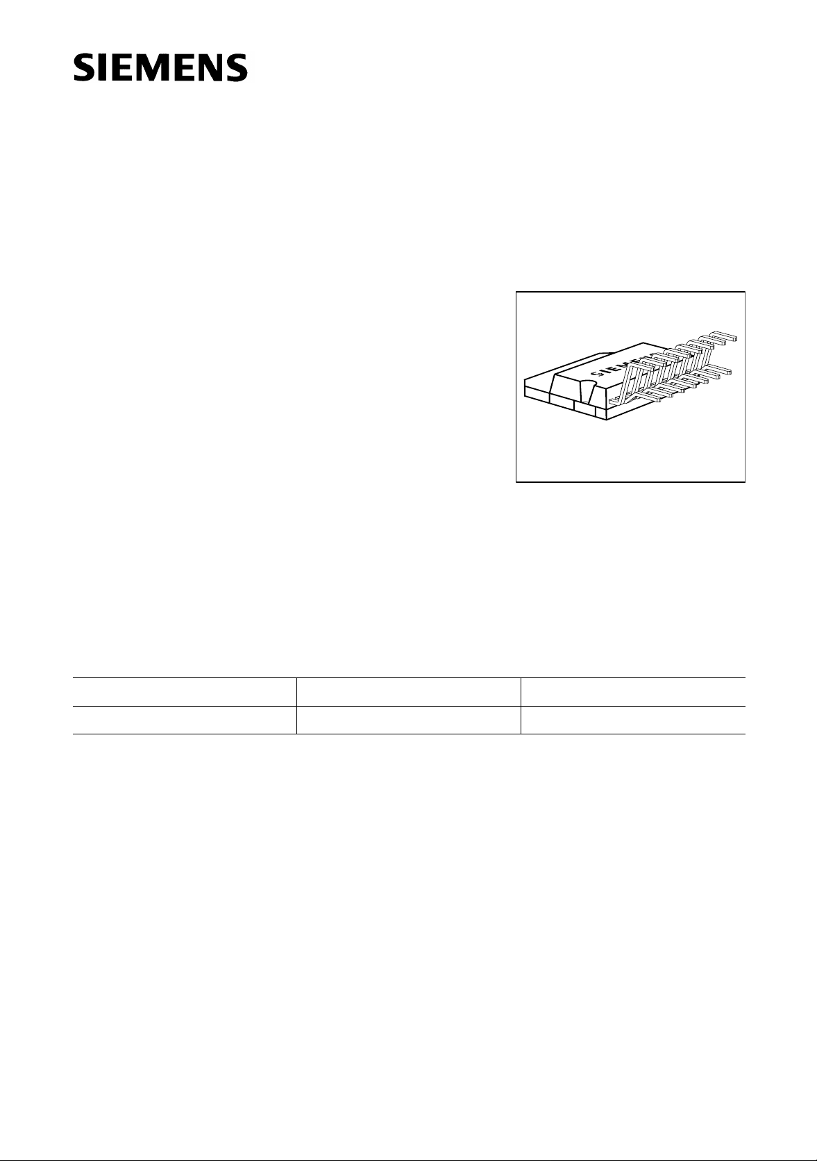
2.5-A High Performance Smart Power
Stepper-Motor Driver with Diagnostic Interface
Overview
Features
• Single phase driver for stepper motor 2.5 A
• Low ON-resistance (typical 0.3 Ω)
• Wide supply range 6 V to 45 V
• Wide current range 10 mA to 3 A
• Fast nominal/actual comparator for micro
stepper mode
• Wide temperature range
• Short circuit protection
• Under voltage shutdown
• Overtemperature shutdown
• Serial diagnostic interface
• Fast freewheeling diodes
• TTL-compatible inputs
TLE 5250
SPT-IC
P-SIP-15-1
Type Ordering Code Package
TLE 5250 Q67000-A9103 P-SIP-15-1
Description
TLE 5250 is a monolithic IC in Smart Power technology for controlling and regulating the
motor current in one phase of a bipolar step ping motor. The re are other appli cations in
driving DC motors and inductive loads that are operated on constant current.
The device has TTL-compatible logic inputs, include s a H-bridge with integrated, fa st
free-wheeling diodes plus dynamic limiting of the motor current by a chopper mode. The
nominal current can be set continuously by a cont rol voltage. Microstep mode can be
produced by applyin g a sinusoidal c ontrol voltage. T wo TLE 5250s, wi th a minimum of
external circuitry and a single supply voltage, form a complete system - that can be
driven direct by an MC- for two-phase, bipolar stepping motors with output current of up
to 2.5 A per phase. The outputs of the IC are internally protected against shorted to
ground, supply voltage and shorted load. The output stages are also disabled by
undervoltage and overtemperature. All fault functions can be detected by the internal
diagnostics, which can be read out serially.
Semiconductor Group 1 1998-02-01
Page 2
PH
DIAG
EN
TLE 5250
151
S
V
Q1
Q1
GND
Sense
Sense
Q2
S
V
Q2
AEP01471
RS
ACT
NOM
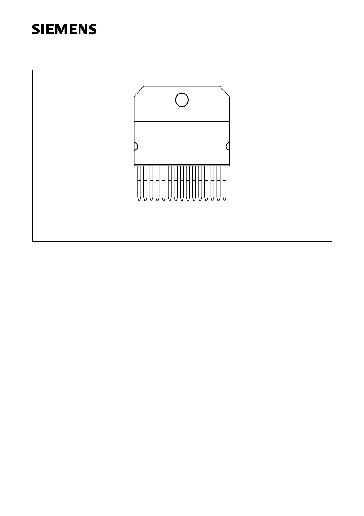
Figure 1 Pin Configuration (top view)
Semiconductor Group 2 1998-02-01
Page 3
TLE 5250
Pin Definitions and Functions
Pin No. Symbol Function
1 DIAG Open-drain diagnostics output
2 PH Input for determining source/sink on outputs Q1 and Q2; when
Enable = Low, this pin serves as clock input for reading out
diagnostics
3 EN Input for activating or turning off device (all output transistors
turned off); Enable High = output active, Enable
Low = diagnostics
4, 12
V
S
Supply voltage of IC
5, 6 Q1 Power output with integrated free-wheeling diodes
7, 9 Sense Actual-current output: shared, open-source output of sink
transistors
8 GND Ground
10, 11 Q2 Power output with integrated free-wheeling diodes
13 RS Determines turning back on of sink transistor by internally
driven, external RC element or external TTL trigger signal
14 NOM Input for reference potential (nominal current) for nominal/
actual comparator
15 ACT Input for actual current for nominal/actual comparator
Semiconductor Group 3 1998-02-01
Page 4
TLE 5250
Charge Pump
S
412
S
VV
Bandgap/Bias
-6 V
S
V
Driver 2
T2T1
Driver 1
Q1
5
6
-1.5 V
S
V
+
-
Q1 High
H-Bridge
-1.5 V
S
V
-
+
Q2 High
Q2
10
Output Stage
3 V
+
3 V
-
+
Q2 Low
Q1 Low
11
-
5 V
-
+
G on T4
5 V
-
+
G on T5
Driver 4
T4
T3
Driver 3
AEB01468
9
Sense
7
Sense
GND
T1
T2
T3
T4
CC1
CC2
S
V
Bias
V
V
16
Cooling Pin
Undervoltage
Overtemperature
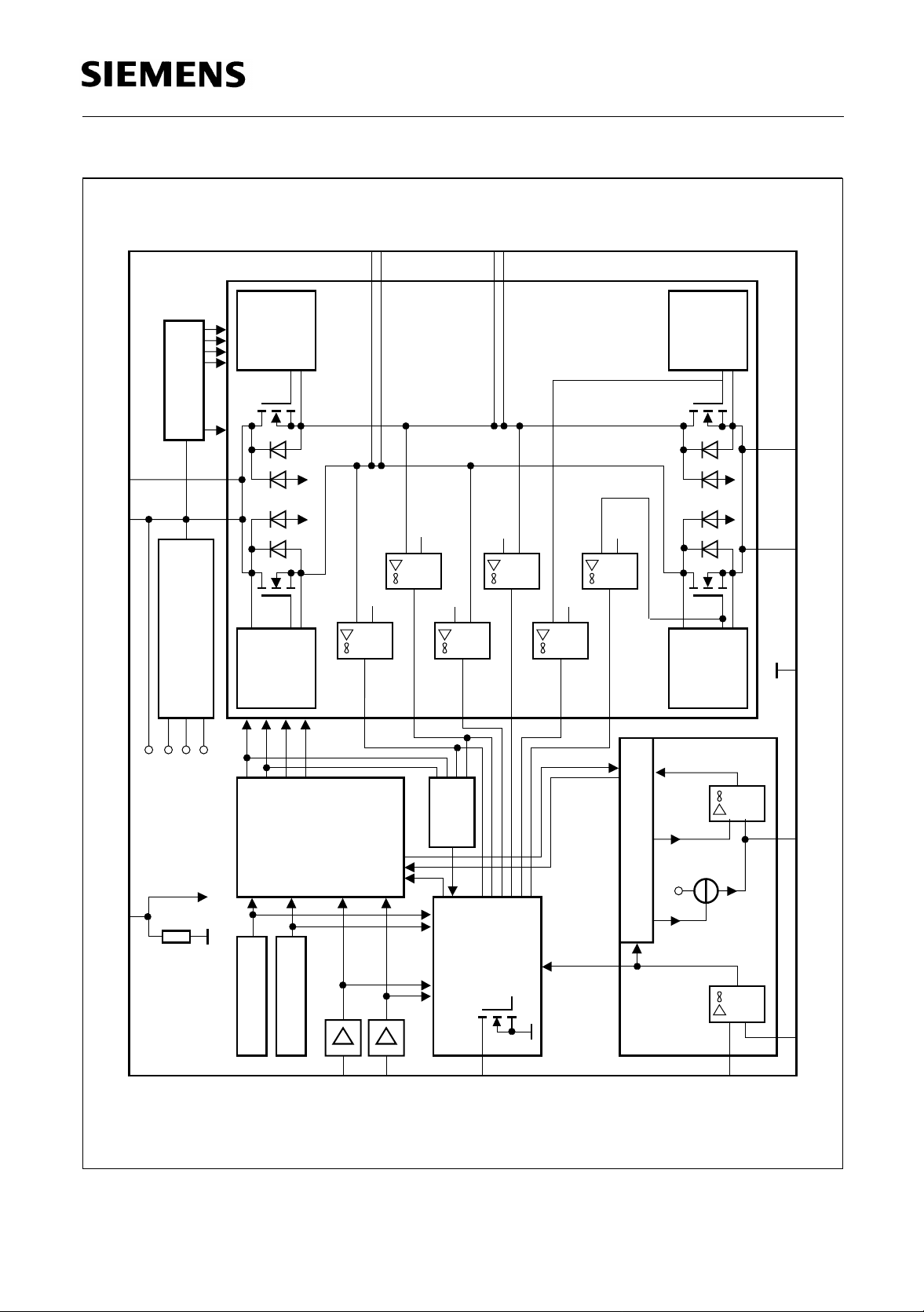
Figure 2 Block Diagram
Logic
Functional
3
Enable
2
Phase
Overload
Diagnostics
Logic
1
Diagn
Chop Logic
ref
V
Charge
Off/Ι
Nom/Act
PWM Logic
1 mA
Comp
14
-
+
+
-
Nominal
13 8
15
Actual RC/Sync
Semiconductor Group 4 1998-02-01
Page 5

TLE 5250
Application
Two TLE 5250 drivers are required to operate a bipolar stepping motor. To implement
full-step operation, a squarewave voltage with the required stepping frequency is applied
to the phase in put of the upper drive r, and the s ame squarewave voltage, bu t offset in
phase by 90°el, to the phase input of the lower driver. Motor-current limiting is produced
by a DC signal that is applied to both nominal-current inputs. In microstep operation the
nominal current tracks sinusoidally and synchronously with the required stepping
frequency. This produces a sinusoidal current in the motor windings to ensure very
smooth running and a high stepping frequency. If an instantaneous nominal value (sine
or cosine) is held on the second driver, it is possible to set a certain angle of rotation while
the motor is stationary. The motor current produced by this depends on nominal voltage
and sense resistance (normally 0.5 Ω), i.e.
V
M
V[]
=
---------------------- -
I
nom
R
S
V[]
Ω[]
The actual voltage should be thoroughly filtered for precise current regulation, especially
in microstep operation. So the actual input is accessible, and an RC element is
R
necessary between the Sense output and Actual input. The resistance
should
R
correspond to the internal resistance of the nominal-current input-voltage source to
prevent additional voltage offset on the nominal/actual comparator.
Circuit Description
Outputs
Outputs Q1 and Q2 are fed by push-pul l output stages. Four integrated free-wheeli ng
diodes referred to ground or the supply voltage protect the integrated circuit against
reverse voltages from an inductive load.
Enable and Phase
V
Outputs Q1 and Q2 ca n be dis abled by a voltage
V
sink transistors are enabled by
Inh
≥ 2V.
of ≤ 0.8 V on the Enable pin. The
Inh
The voltage on the Phase input d etermines the phase of the ou tput current. Ou tput Q1
V
acts as a sink for
For output Q2 this is reversed: sink for
≤ 0.8 V and as a source for VPh≥ 2V.
Ph
V
≥ 2 V and source for VPh≤ 0.8 V.
Ph
The sink transistors are chopped. Low signal on the Enable pin plus a clock signal on the
Phase pin enable readout of the multiplexer.
Semiconductor Group 5 1998-02-01
Page 6

TLE 5250
Nominal-Current Input
The peak current in the motor windi ng is defined by the voltage on the Nomin al input.
This is compared by a fast comparator to the voltage drop on the actual-current sensor.
If the nominal current is exceeded, the sin k transistors of the output s are turned off by
the logic.
RC/Sync Input
The outputs are turned on by the signal applied to the RC input. Synchronization is
possible by TTL signal or chopper mode with an external RC combination.
Chopper Mode
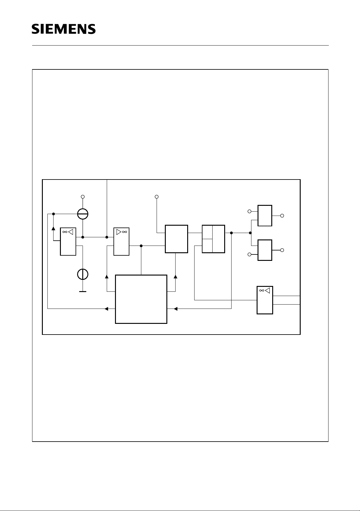
After the supply voltage is applied, capacitor CT is charged with constant current of
1 mA. A regulator limits the maximum voltage on the capacitor to 2.3 V. As a result of the
rising current in the motor winding, the voltage on the actual sensor increases. Once the
value defined by the nominal-current input is exceeded, the fast c omparator resets an
RS flipflop. Thus sink transistors T3 and T4 are turned off by the logic. The charge
current is turned off and the parallel RT discharges CT.
The internal logic is designed so that capacitor CT is always charged before the
discharge operation is triggered. This guarantees a constant charge time, even for very
small coil currents (see Figure 7).
Sync Operation
If a sync signal with TTL le vel is app lied to the RC inp ut, the nega tive edge will set the
RS flipflop - by way of the combined Schmitt trigger and monoflop - if the voltage on the
current sensor is smaller than the nominal value on the nominal-current input. As in
chopper mode, the appropriate output transistors conduct. They are again turned off by
resetting the RS flipflop when the voltage on th e current sensor becomes gre ater than
the nominal value (see Figure 8).
Output-Stage Control
This part of the circuit handles turn-off of the output stages when the output is shorted to
ground. There is sep arate current mon itoring for this purpos e in the s ource trans istors.
The temperature of the output stages is also monitored. If this exceeds 175 °C, all output
stages are turned off, and then turned on again when the temperature drops.
Undervoltage also causes turn-off of the transistors in the output stages. These possible
fault states are stored in the diagnostics register.
Semiconductor Group 6 1998-02-01
Page 7
TLE 5250
Diagnostics
The information from the dif ferent parts of the circuit is colle cted in the di agnostics a nd
stored in the fault logic. The information is read out on the Diagnostics output (open
collector).
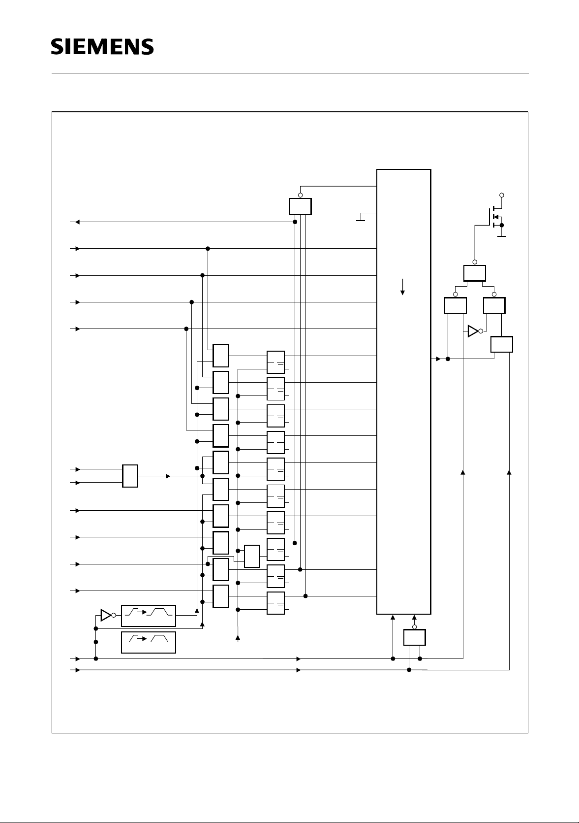
The fault logic consists of a 16-bit multiplexer that switches information in three
categories through to the Diagnostics output.
Bit 0 always appears inv erted on DIAG when EN is High. This means that, if there is
overcurrent on the upper transistor, undervoltage or overtemperature, it will be signaled
immediately on the Diagnostics output. DIAG changes from High to Low.
Bit 1: check bit.
Bits 2, 3, 4 and 5 ind icate th e mome ntary sta tus of t he comp arator s on the two outpu ts
(see Figure 2). Cha nges in the statu s of the comparator s for output monitoring can be
observed on DIAG when EN is Low and the counter of the multiplexer is on 2, 3, 4 or 5.
This is necessary for detecting underload.
Bits 6, 7, 8, 9
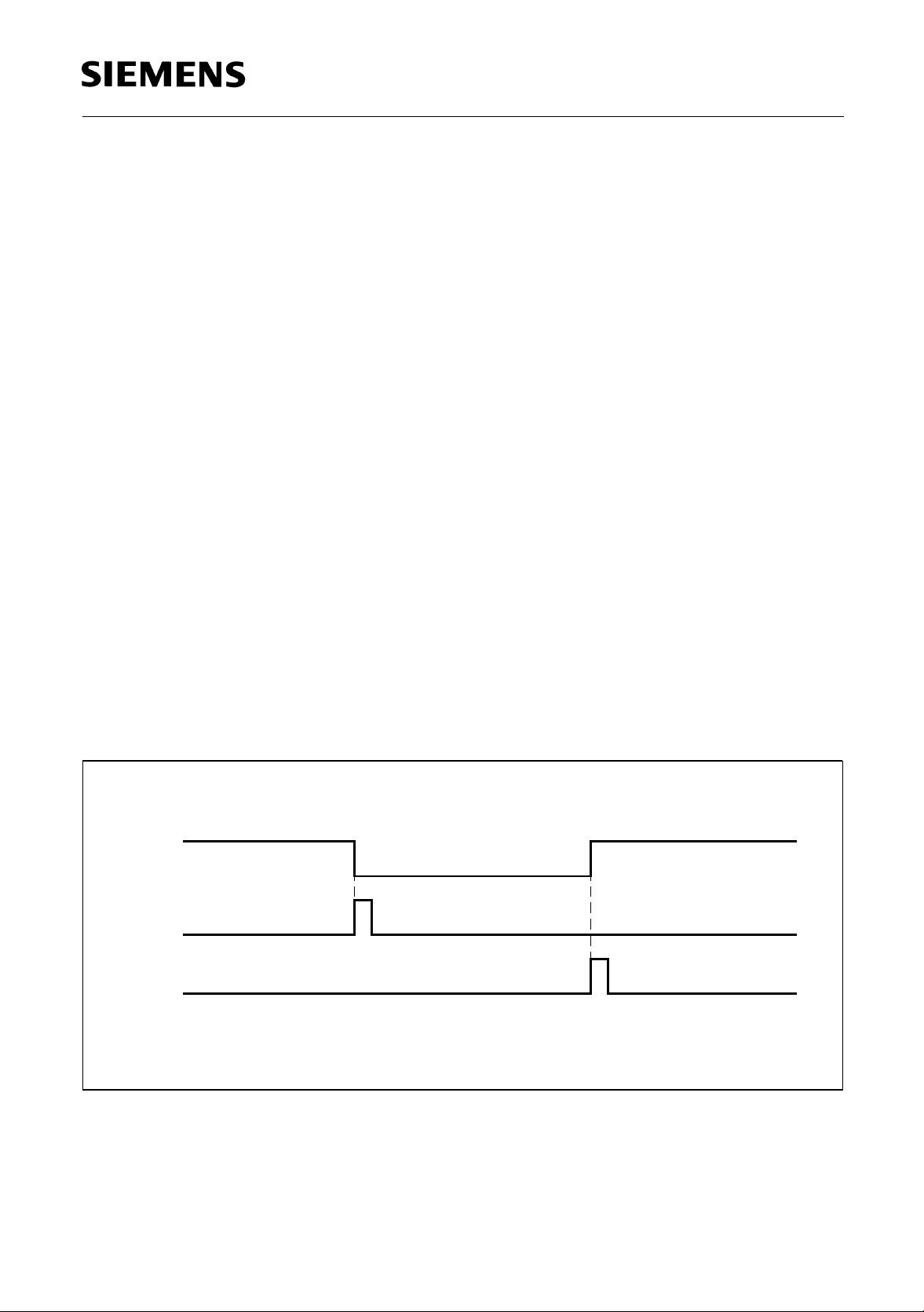
The monoflop generates a s hort s trobe sign al w hen the EN edge changes from High to
Low. The status of the comparators for outp ut monitoring is stored with this si gnal and
can be read out in bits 6, 7, 8 and 9.
When Enable is Low, the Phase input is used as a cl ock input. As the edge rises, an
internal counter is incremented and the corresponding channel of the multiplexer is
switched through. As the edge f alls , the sign al is outp ut in verte d. Whe n Enab le is Hi gh,
the counter is reset to zero.
EN
Strobe
Reset
AED01467
Figure 3
Semiconductor Group 7 1998-02-01
Page 8

TLE 5250
Bits 10, 11
With these bits it is possible to detect the status of the gate voltages of the lower outputstage transistors T3 and T4 . Bit 10: status for EN edge transition . Bit 11: whether the
lower transistor has at all been turned on.
Bit 12 indicates wh ether the nominal/actua l comparator has sw itched. The compar ator
switches when the output current is regulated.
Bits 13, 14, 15
These bits indicate the presence of overcurrent, undervoltage or overtemperature. A
fault is ORed and output direct by bit 0 on DI.
When the multiplexer is read out, bits 0 through 15 are output once non-inverted (Phase
= Low) and once inverted (Phase = High).
Bit Assignment in Error Register
Bit 0 = High for overtemperature/undervoltage/overcurrent
Bit 1 = always High
Bit 2 = High when sink transistor Q1 turned on
Bit 3 = High when sink transistor Q2 turned on
Bit 4 = High when source transistor Q1 turned on
Bit 5 = High when source transistor Q2 turned on
Bits 2-5 = momentary states for readout
Bit 6 = bit 2 state for falling edge of Enable signal
Bit 7 = bit 3 state for falling edge of Enable signal
Bit 8 = bit 4 state for falling edge of Enable signal
Bit 9 = bit 5 state for falling edge of Enable signal
Bits 6-10 represent status of outputs for negative change in edge of Enable signal
Bit 11 = High if gate-source voltage of sink transistors is > 5 V at moment of readout
Bits 11-15 are set if event occurs during switching (Enable = High)
Bit 11 = High if sink transistor V
GS
> 5 V
Bit 12 = High if actual current lower than nominal current
Bit 13 = High if overcurrent detected on source transistors
Bit 14 = High if undervoltage detected
Bit 15 = High if thermal link tripped
The memories are erased by a rising edge on the Enable input.
Semiconductor Group 8 1998-02-01
Page 9
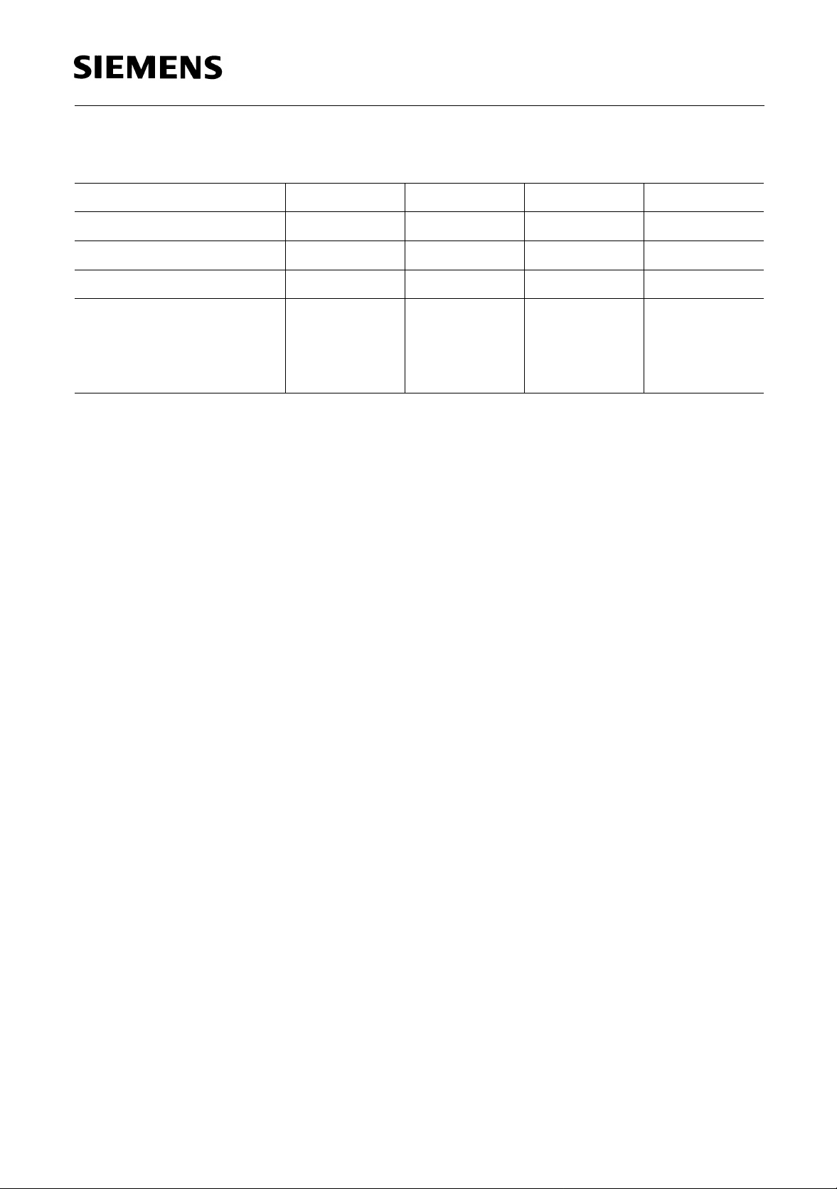
Logic Assignment: Control Inputs, Output Transistors
Enable L L H H
Phase L H L H
Output Q1 / / L H
Output Q2 / / H L
TLE 5250
Transistor T1
Transistor T2
Transistor T3
Transistor T4
X
X
X
X
X
X
X
X
L = Low voltage level, input open
H = High voltage level
X = transistor turned off
– = transistor conducting
– = transistor conducting, switched in current limiting
/ = output high-impedance
X
–
–
X
–
X
X
–
Semiconductor Group 9 1998-02-01
Page 10
RC/Sync
TLE 5250
5 V 5 V
1 mA
-
1.8 V
+
0.8 V
2.3 V
Deadtime
Comparator
+
-
Charge-Current
and SwitchingThreshold
Control,
Reset-Pulse
Generation
DT Output
DFF
DQ
T
R
N/A Output
RS FF
S
R
Input
T3
Q
Input
T4
FF
QRS
&
&
Nom/Act
Comparator
+
-
AES01469
Gate
T3
Gate
T4
Nominal
Actual
Figure 4 PWM Logic
Semiconductor Group 10 1998-02-01
Page 11
Overcurrent Flag
Q1 Low Status
Q2 Low Status
Q1 High Status
Q2 High Status
GOn T3
GOn T4
Nom/Act Stat. Act>Nom->High
Overcurrent T1/T2 Status
Undervoltage Status
Overtemperature Status
Enable
Phase
_
<
1
GOn Status
Monoflop
Monoflop
Strobe
Latch
Reset
TLE 5250
Error Status
Continuous
<
_
1
&
&
&
&
&
&
&
&
&
&
QQRS
QQRS
QQRS
QQRS
QQRS
QQRS
QQRS
QQRS
_
<
1
QQRS
S
Q
RQ
Check Bit Low
Q1 Low Status
Continuous
Q2 Low Status
Continuous
Q1 High Status
Continuous
Q2 High Status
Continuous
Q1 Low Status
Q2 Low Status
Q1 High Status
Q2 High Status
Gon Status
Gon Status
Actual Current up
to Nominal Latched
Overcurrent T1/T2
Undervoltage
Overtemperature
Strobed
Strobed
Strobed
Strobed
Strobed
Latched
Latched
Latched
Latched
0
M
U
X
1
C
h
a
n
2
n
e
l
3
4
5
6
MUX
7
16-to-1
8
Sequential
Multiplexer
9
10
11
12
13
14
15
Reset Clock
Diagn. Pin
1
1
Q
<
_
1
1
&
AES01470
Figure 5 Diagnostics Logic
Semiconductor Group 11 1998-02-01
Page 12
TLE 5250
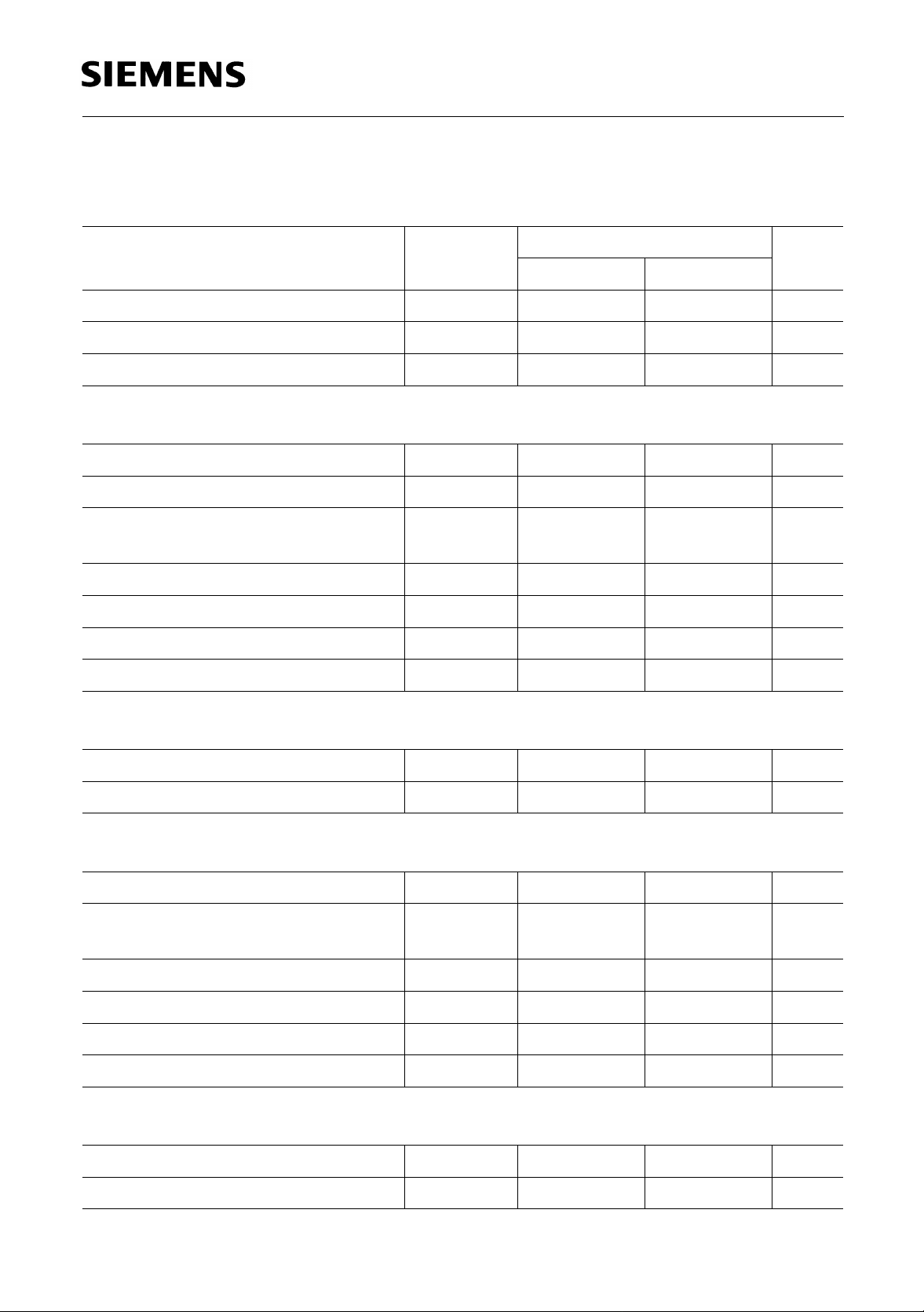
Absolute Maximum Ratings
T
= – 40 to 150 °C
J
Parameter Symbol Limit Values Unit
min. max.
Supply voltage
Supply current
Peak curre nts on outputs
Diode Forward Currents
Diode to +
V
S
Diode to sense
Output current on
actual-current pin
Voltage on actual-current pin
Ground current, pin 6
Chip temperature
Storage temperature
Thermal Resistances
V
S
I
S
I
Q
I
FH
I
FL
I
Act
V
Act
I
GND
T
C
T
stg
– 0.3 45 V
03A
– 3 3 A
–3A
–3A
–3A
– 0.3 5 V
–3A
– 40 150 °C
– 125 °C
Junction to ambient
Junction case
Operating Range
Supply voltage
Input voltage
Enable, Phase, RC/Sync
Voltage on nominal pin
Voltage on actual pin
Output current Q1, Q2
Junction temperature
Enable and Phase Inputs
H input voltage
L input voltage
R
R
V
V
V
V
I
Q
T
V
V
thjA
thjC
S
I
NOM
ACT
J
IH
IL
–70K/W
–3K/W
640V
– 0.3 5.5 V
– 0.3 2 V
–2V
– 2.5 2.5 A
– 40 150 °C
2–V
–0.8V
Semiconductor Group 12 1998-02-01
Page 13
TLE 5250
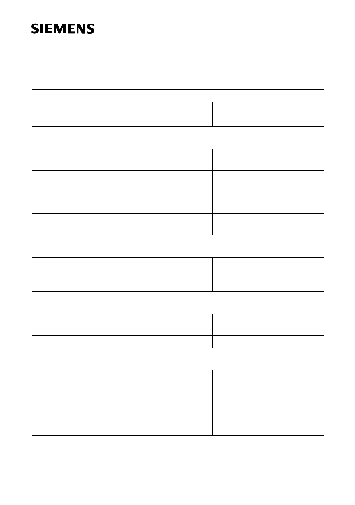
Characteristics
V
= 6 to 25 V; TJ ≤150 °C
S
Parameter Symbol Limit Values Unit Test Condition
min. typ. max.
Supply current
Output Q1, Q2
Turn-on resistance of output
transistors
Phase deadtime
Diode forward voltage
output
V
to +
S
Diode forward voltage
actual-current pin to output
Nominal Current
Input current
Offset voltage measured for
0 V actual/nominal pin
I
S
R
DS ON
t
D
V
FQ
– ––1.5V
I
I8
V
I(8 – 4)
– – 11 mA Enable = High
0.3 – 0.5 Ω I = 2.5 A, 150 °C
–10–µs–
––1.5VIFH = 2.5 V
I
012µA–
– 4 – 8 mV –
= 2.5 V
FH
Actual Current
Turn-off delay of nom/act
comparator
Common-mode error
RC/Sync
Sync frequency
Trigger threshold
lower
upper
Maximum charge voltage
t
V
f
V
V
V
d
Comm
tL
tH
Chm
––0.5µs–
– 5 – 10 mV –
–20100kHz–
0.8
1.7
–
–
1
2
V
V
–
–
2.2 2.3 2.4 V R = 39 kΩ
C = 820 pF
Semiconductor Group 13 1998-02-01
Page 14
TLE 5250
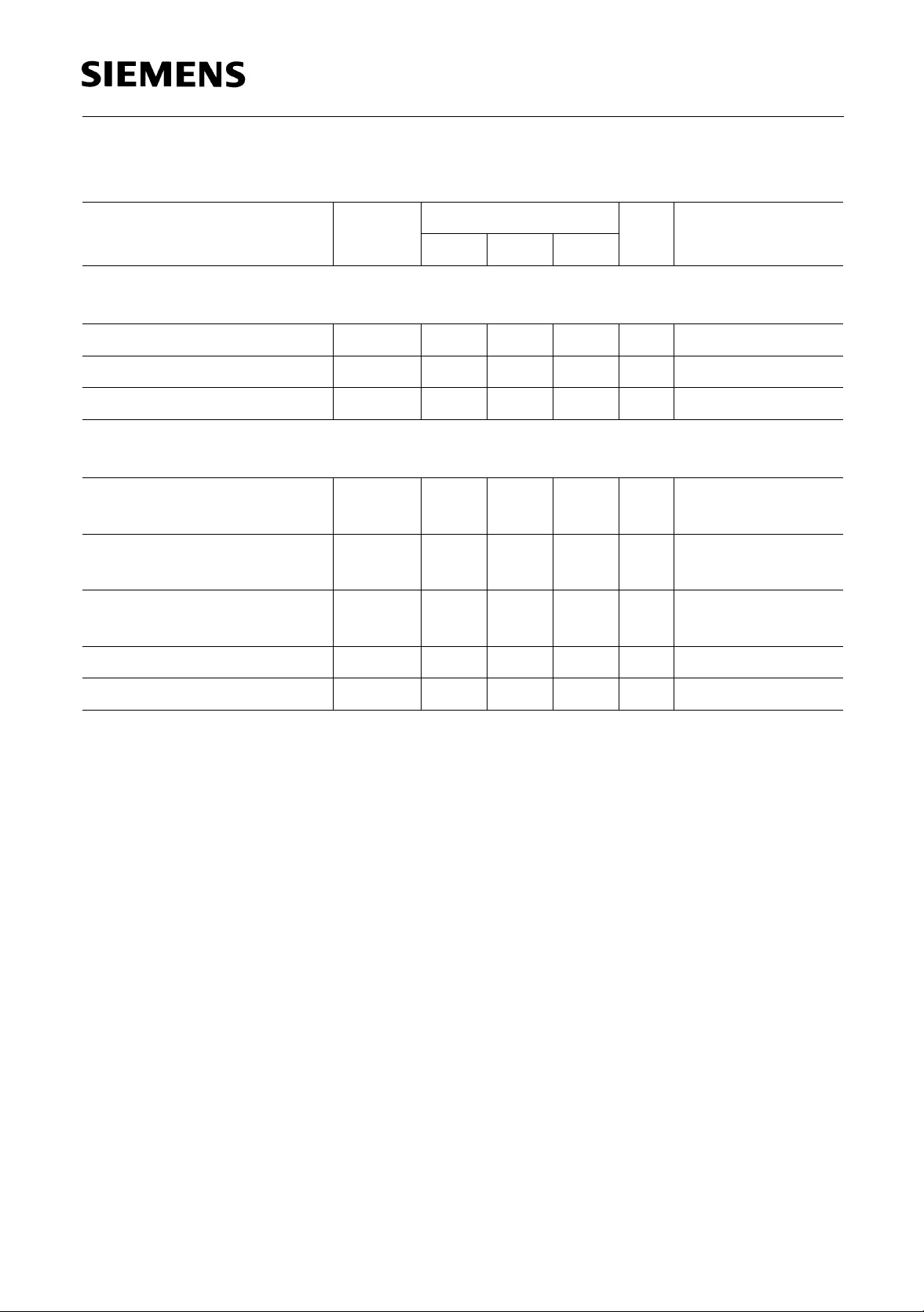
Characteristics (cont’d)
Parameter Symbol Limit Values Unit Test Condition
min. typ. max.
Undervoltage Cutout
Disable
Enable
Hysteresis
Diagnostics Output
Activating delay
(Enable High → Low)
Delay phase low to high
Delay phase high to low
Output voltage low
Leakage current high
V
UDIAG
V
UEN
V
UH
t
def
t
ddr
t
ddf
V
Diag
I
Diag
4––V–
––5.3V–
––400mV–
– – 400 ns –
– – 500 ns Enable = Low
V
> 5.5 V
S
– – 450 ns Enable = Low
V
> 5.5 V
S
––0.4VIQL = 5 mA
––10µA VQH = 5 V
Semiconductor Group 14 1998-02-01
Page 15
TLE 5250
5 V
R
Ω2 k
100 nF 22 µF
V
Batt
(Tantalum)
Cooling Pin
Diagnostics
GND
V
S
1 nF
Q1
Phase
Cµ
TLE 5250
M
Enable
R
N
Nominal
Ω1 k
C
N
Actual RC/Sync. Sense
R
T
39.2 k Ω
C
T
820 pF68 pF
Q2
1 nF
R
R
R
K
1 k Ω
C
F
680 pF
R
S
Ω0.5
AES01472
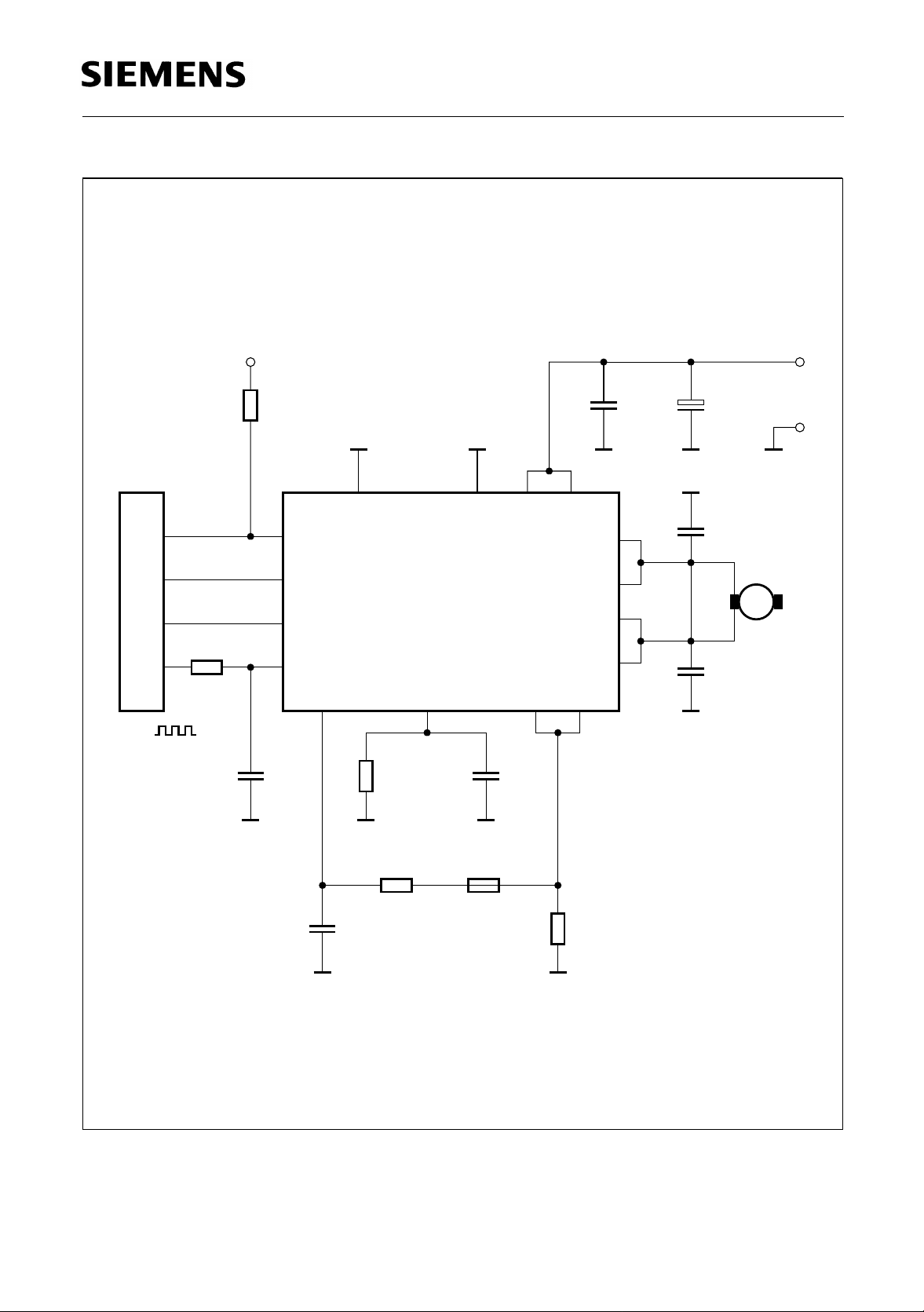
Figure 6 Application Circuit 1
Semiconductor Group 15 1998-02-01
Page 16
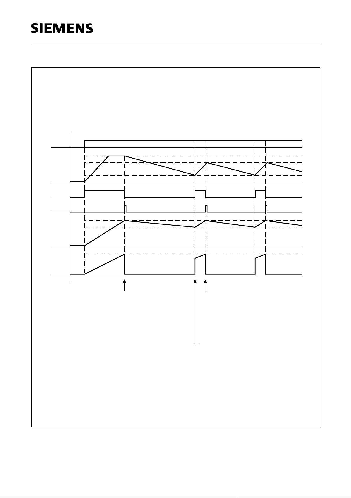
TLE 5250
Phase = High or Low
Enable
2.3 V
1.8 V
V
RC/Sync
QRSFF
SI OUT
Coil
Current
Actual
Voltage
0.8 V
Discharge operation is started
when nominal current is reached.
is discharged by
C
T
.
R
T
Voltage on RC/Sync was limited
internally to 2.3 V in charge
operation.
When coil current reaches nominal
value, sink transistor is turned off.
Independently of this, RC element is
charged up to 1.8 V and then
discharged.
Charge operation is controlled by
deadtime comparator. RC element is
charged with 1mA.
AED01475
Figure 7 Chopper Mode with External Capacitor CT and Resistor RT
Semiconductor Group 16 1998-02-01
Page 17
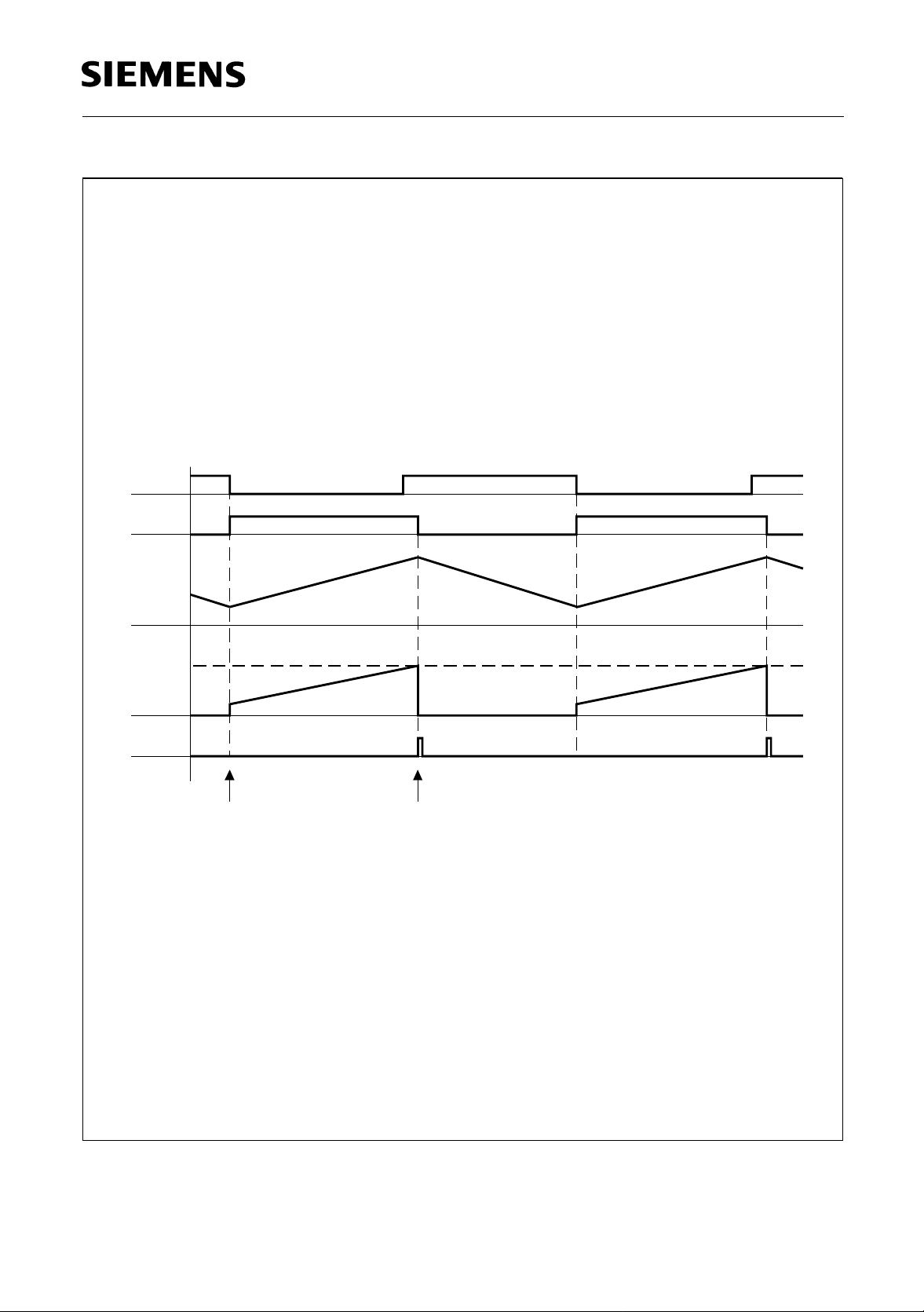
TLE 5250
RC/Sync
QRSFF
Coil
Current
Actual
Voltage
N/A
Output
Falling edge turns on
sink transistor.
Nominal Voltage
Sink transistor is turned
off again when nominal
voltage is reached.
AED01476
Figure 8 Synchron Mode
Semiconductor Group 17 1998-02-01
Page 18
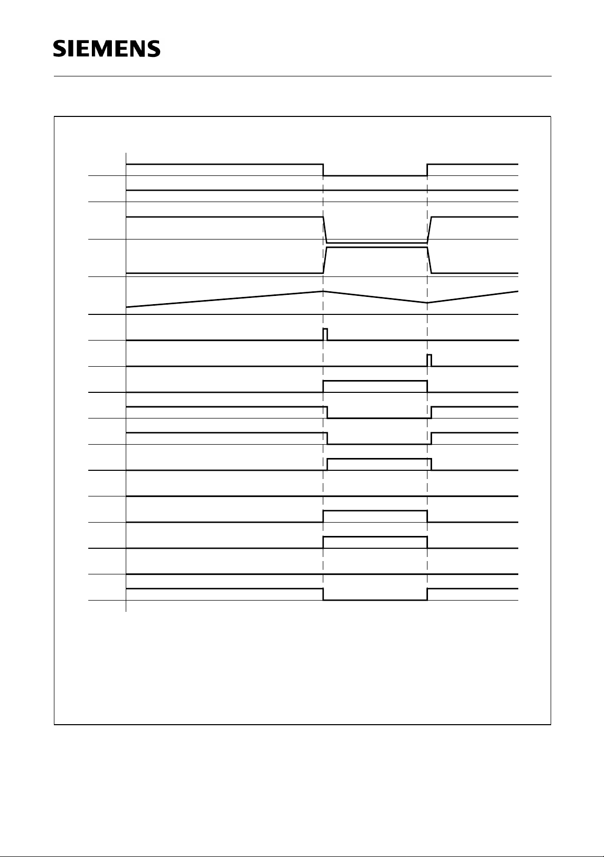
TLE 5250
EN
PH
Q1
Q2
Ι
L
Strobe
Reset
Bit 2
Bit 3
Bit 4
Bit 5
Bit 6
Bit 7
Bit 8
Bit 9
Bit 0
Q1 Low
Q2 Low
Q1 High
Q2 High
Q1 Low Strobed
Q2 Low Strobed
Q1 High Strobed
Q2 High Strobed
AED01477
For inductive load and faultfree operation,
diagnostics when read out must show
bit 2 inverted to bit 6
bit 3 inverted to bit 7
bit 4 inverted to bit 8
bit 5 inverted to bit 9
Figure 9 Response to Inductive Loads
a) Normal Operation (no current regulation)
Semiconductor Group 18 1998-02-01
Page 19
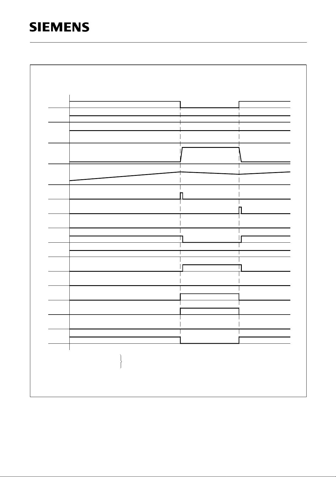
TLE 5250
EN
PH
Q1
Q2
Ι
L
Strobe
Reset
Bit 2
Bit 3
Bit 4
Bit 5
Bit 6
Bit 7
Bit 8
Bit 9
Bit 0
Q1 Low
Q2 Low
Q1 High
Q2 High
Q1 Low Strobed
Q2 Low Strobed
Q1 High Strobed
Q2 High Strobed
Bit 2 identical to bit 6
Bit 4 identical to bit 8
AED01478
= fault
Figure 10 Response to Inductive Loads
V
b) Q1 Shorted to +
Semiconductor Group 19 1998-02-01
(Phase = High)
S
Page 20
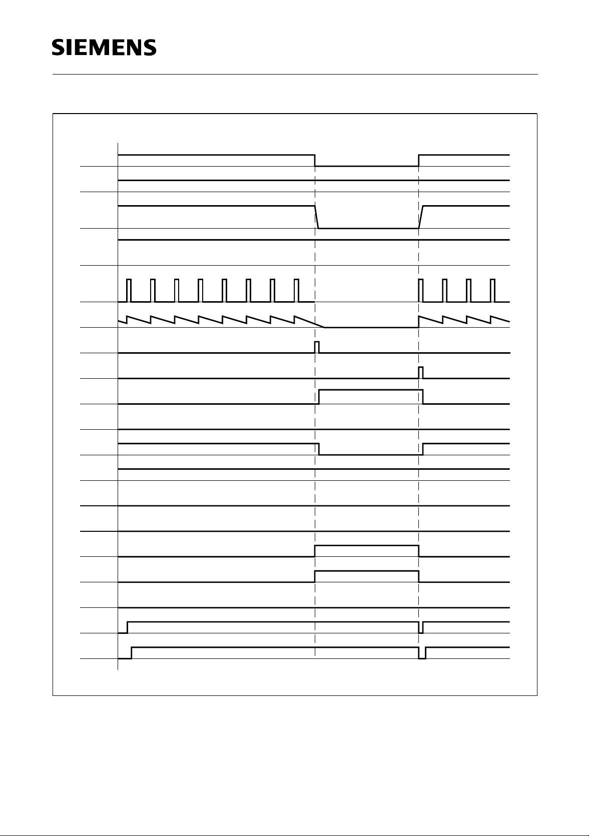
EN
PH
Q1
Q2
Ι
L
RC/Sync
TLE 5250
Strobe
Reset
Bit 2
Bit 3
Bit 4
Bit 5
Bit 6
Bit 7
Bit 8
Bit 9
Bit 10
Bit 11
Bit 12
AED01479
Figure 11 Response to Inductive Loads
V
c) Q2 Shorted to +
Semiconductor Group 20 1998-02-01
(Phase = High)
S
Page 21
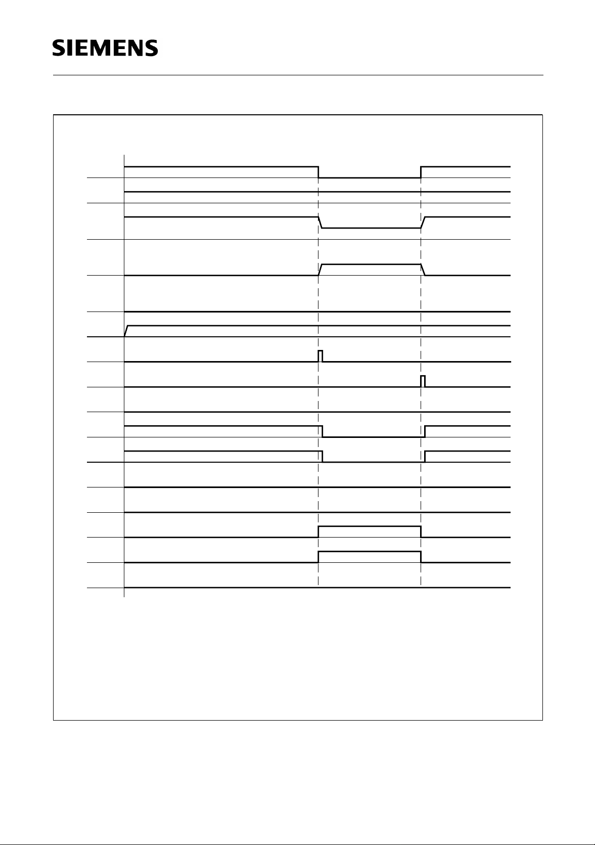
TLE 5250
EN
PH
Q1
Q2
Ι
L
RC/Sync
Strobe
Reset
Bit 2
Bit 3
Bit 4
Bit 5
Bit 6
Bit 7
Bit 8
Bit 9
Ι
= 0
L
Indication of low load: bit 2 = bit 3
bit 4 = bit 5
while Enable = Low
And conditions
bit 2 = /bit 6
bit 3 = /bit 7
bit 4 = /bit 8
bit 5 = /bit 9 are not all satisfied
AED01480
Figure 12 Response to Inductive Loads
d) Low Load
Semiconductor Group 21 1998-02-01
Page 22
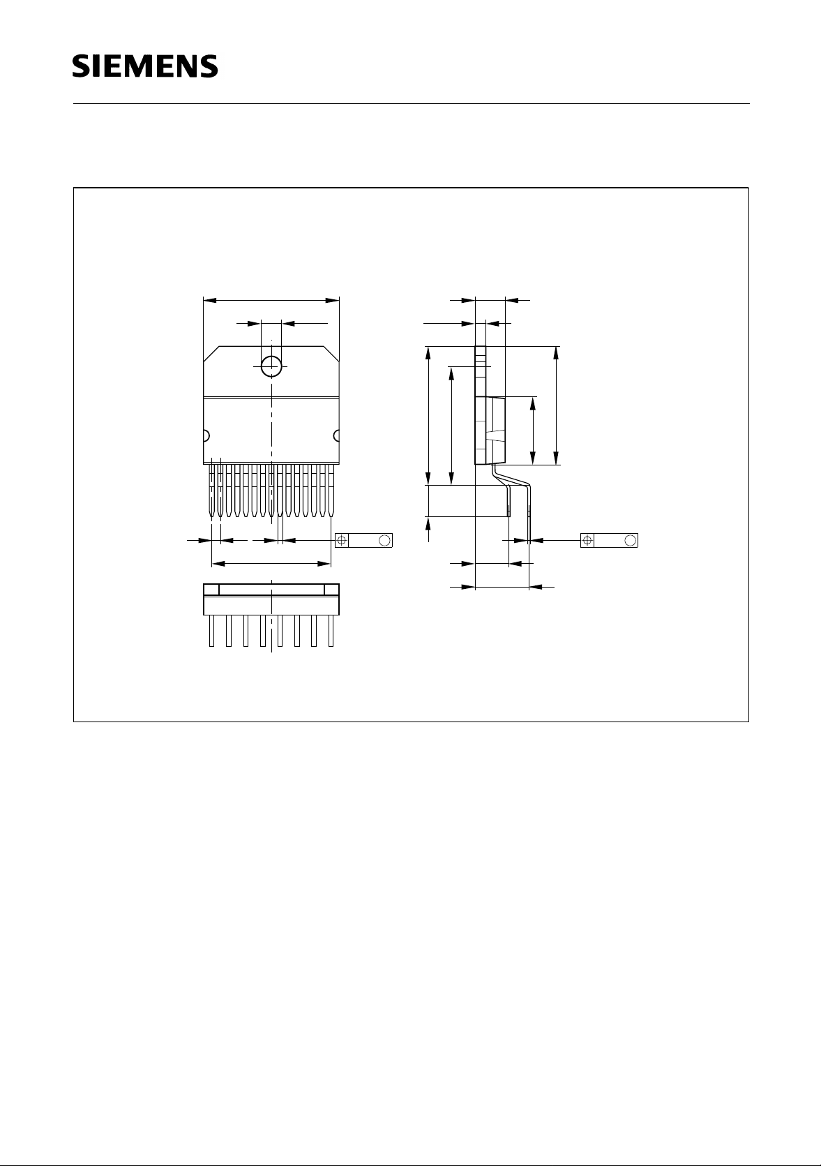
Package Outlines
P-SIP-15-1
(Plastic Single In-Line)
TLE 5250
20
1
1.27 0.69
17.78
±0.3
3.8
±0.06
±0.1
15
0.25
M
15x
±0.08
1.52
±0.25
21 max
17.78
±0.33
4.14
4.62 max
4.29
9.37
+0.15
10.7
0.5
±0.15
17.5
±0.13
0.61
M
15x
Sorts of Packing
Package outlines for tubes, trays etc. are contained in our
Data Book “Package Information”.
GPI09015
Dimensions in mm
Semiconductor Group 22 1998-02-01
 Loading...