

Page 1
TLE 5226 G
Smart Quad Channel Low-Side Switch
Features Product Summary
• Low ON-resistance 2 x 0.2 Ω , 2 x 0.35 Ω (typ.)
• Power - SO 20 - Package with integrated
cooling area
• Overload shutdown
Supply voltage V
Drain source voltage V
On resistance R
• Selective thermal shutdown
• Status monitoring
Output current I
• Overvoltage protection
• Shorted circuit protection
• Standby mode with low current consumption
• µC compatible input
• Electostatic discharge (ESD) protection
Application
• All kinds of resistive and inductive loads (relays,electromagnetic valves)
• µC compatible power switch for 12 and 24 V applications
• Solenoid control switch in automotive and industrial control systems
General description
Quad channel Low-Side-Switch (2x5A/2x3A) in Smart Power Technology (SPT) with four seperate inputs and four open drain DMOS output stages. The T LE 5226 is fully protected by embedded pr otection functions and designed for automotive and industrial applications.
4.8 - 32 V
S
DS(AZ)max
ON(typ) 1,2
R
ON(typ) 3,4
D 1,2
I
D 3,4
60 V
0.2 Ω
0.35 Ω
2 x 5 A
2 x 3 A
P-DSO-20-10
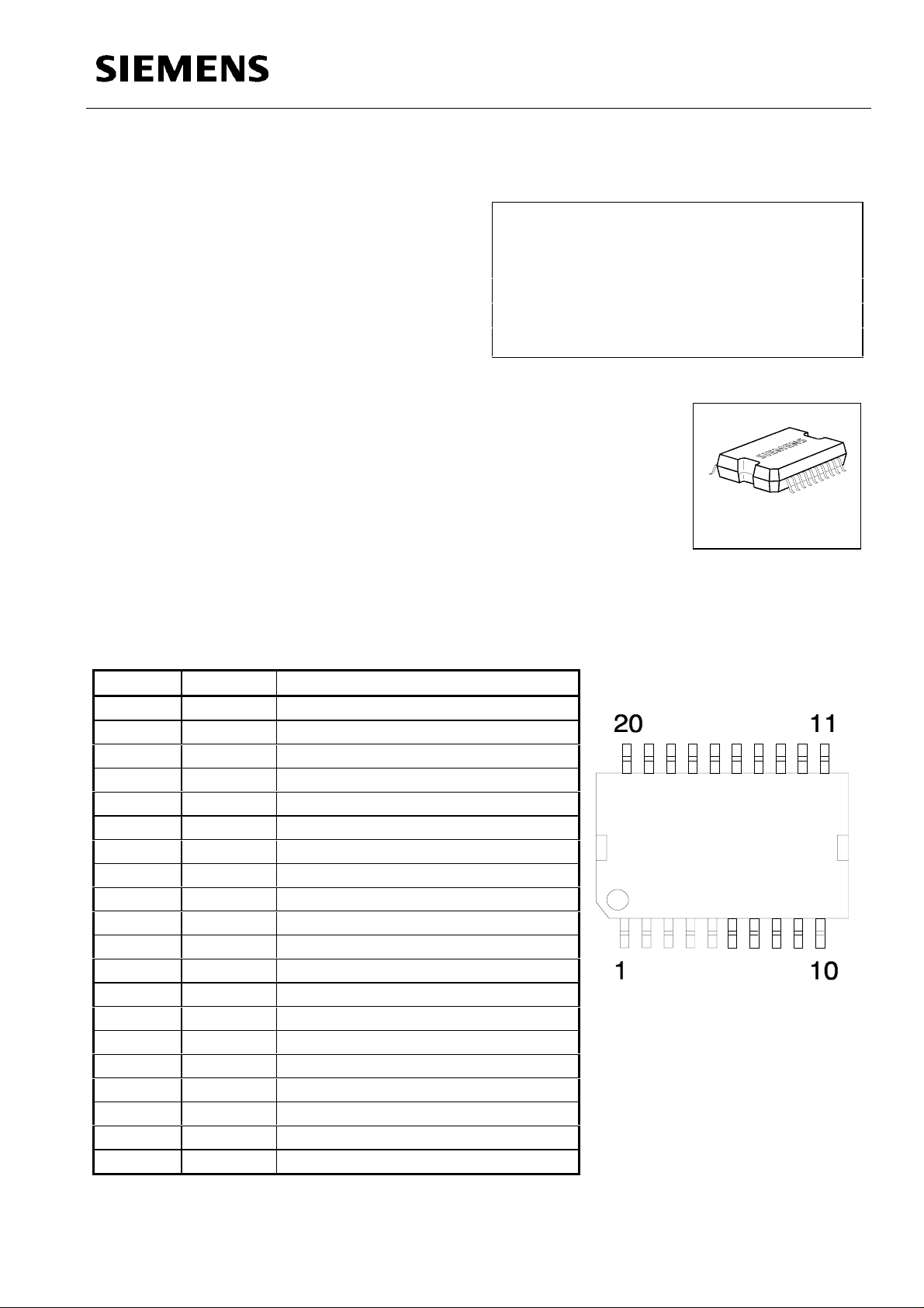
Pin Description Pin Configuration (Top view)
Pin Symbol Function
1 GND Ground
2 OUT1 Power Output channel 1
3 ST1 Status Output channel 1
4 IN4 Control Input channel 4
5 VS Supply Voltage
6 STBY Standby
7 IN3 Control Input channel 3
8 ST2 Status Output channel 2
9 OUT2 Power Output channel 2
10 GND Ground
11 GND Ground
12 OUT3 Power Output channel 3
13 ST3 Status Output channel 3
14 IN2 Control Input channel 2
P - DSO - 20 - 10
15 GND Ground Logic
16 ENA Enable Input for all four channels
17 IN1 Control Input channel 1
18 ST4 Status Output channel 4
19 OUT4 Power Output channel 4
20 GND Ground
Semiconductor Group Page 1998-02-04
1
Page 2
VS
TLE 5226 G
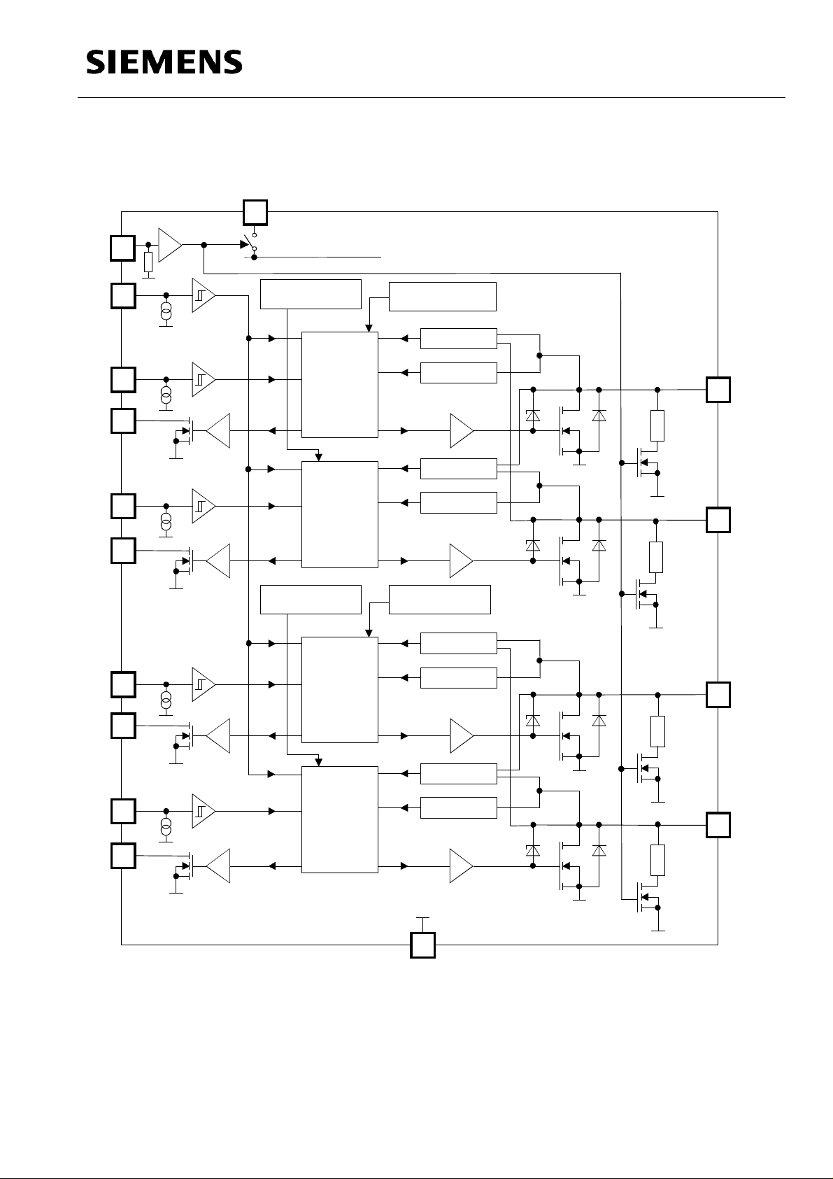
Block Diagram
STBY
ENA
IN1
ST1
IN4
ST4
internal supply
Overtemperature
Channel 4
LOGIC
LOGIC
Overtemperature
Channel 3
Overtemperature
Channel 1
Open Load
Overload
OUT1
RPD
Open Load
Overload
OUT4
RPD
Overtemperature
Channel 2
Open Load
IN2
ST2
IN3
ST3
LOGIC
LOGIC
Overload
OUT2
RPD
Open Load
Overload
OUT3
RPD
GND
Semiconductor Group Page 1998-02-04
2
Page 3
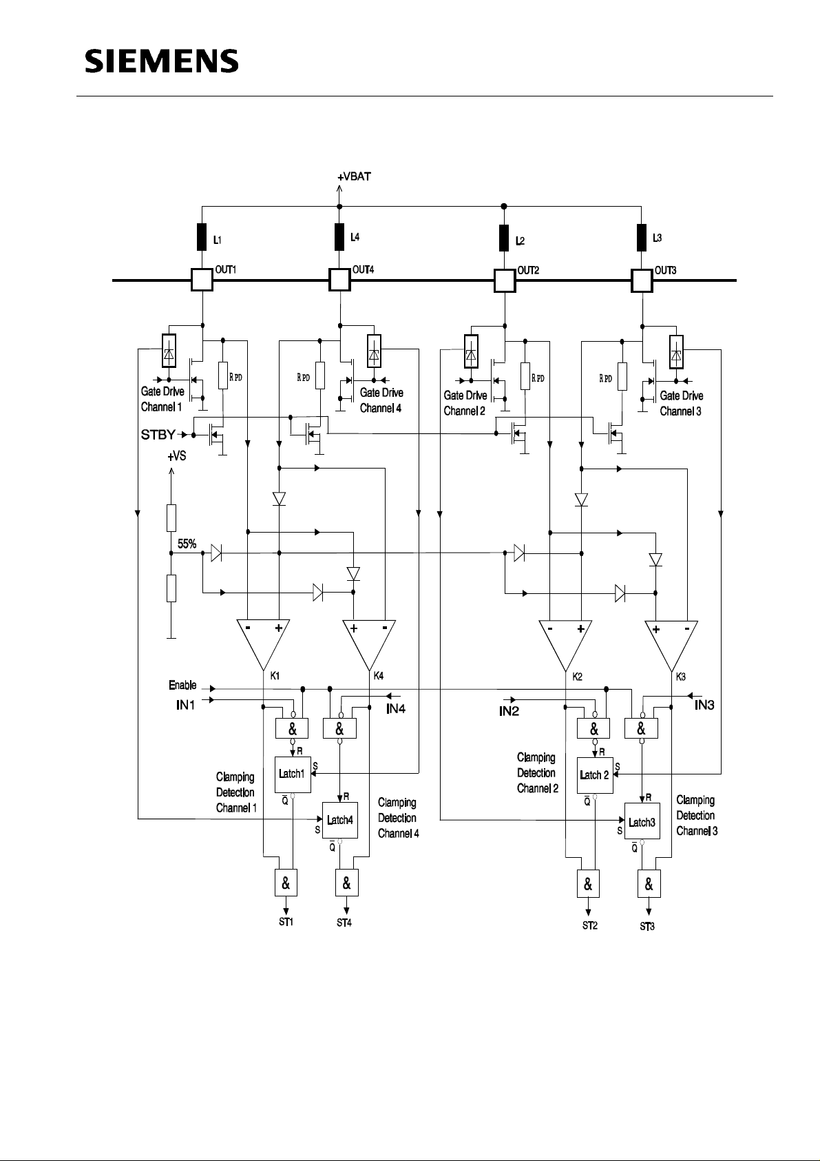
Block Diagram of Open Load Detection
TLE 5226 G
Semiconductor Group Page 1998-02-04
3
Page 4
TLE 5226 G
Maximum Ratings for Tj = – 40°C to 150°C
Parameter Symbol Values Unit
Supply voltage
Supply voltage operational range
Continuous drain source voltage (OUT1...OUT4)
Input voltage IN1 to IN4, ENA
Input voltage STBY
Status output voltage
Operating temperature range
Storage temperature range
Output current per channel
Output current at reversal supply
Status output current
Inductive load switch off dissipation energy Tj = 25°C
Thermal resistance
junction - case
junction - ambient @ min. footprint
junction - ambient @ 6 cm
2
cooling area
V
S
V
S
V
DS
V
IN
V
STBY
V
ST
T
j
T
stg
I
D(lim)
I
D 1,2
I
D 3,4
I
ST
E
AS
R
thJC
R
thJA
-0.3 ... + 40 V
+ 4.8 ... + 32 V
40 V
,
V
ENA
- 0.3 ... + 6 V
- 0.3 ... + 40
- 0.3 ... + 32 V
- 40 ... + 150
°C
- 55 ... + 150
self limited A
- 4
- 2
- 5 ... + 5 mA
50 mJ
K/W
4.5
50
40
A
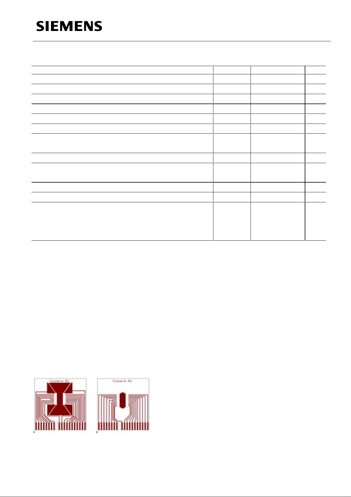
Test board for
6 cm2 cooling area min. footprint
Semiconductor Group Page 1998-02-04
4
Page 5
TLE 5226 G
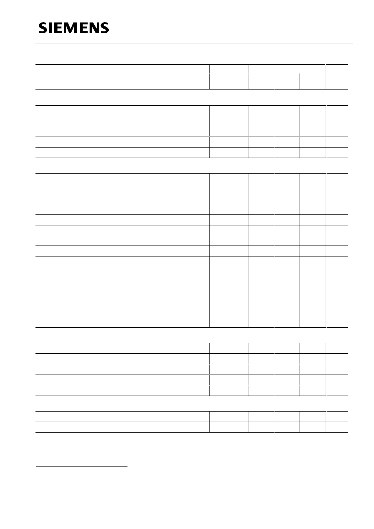
Electrical Characteristics
Parameter and Conditions Symbol Values Unit
VS = 4.8 to 18 V ; Tj = - 40 °C to + 150 °C
(unless otherwise specified)
min typ max
1. Power Supply (V
)
S
Supply current (Outputs ON)
Supply current (Outputs OFF)
V
ENA
= L, V
STBY
= H
Operating voltage
Standby current V
STBY
= L
2. Power Outputs
ON state resistance Channel 1,2 Tj = 25 ° C
I
= 1A; VS ≥ 9.5 V Tj = 125°C
D
ON state resistance Channel 3,4 Tj = 25 ° C
I
= 1A; VS ≥ 9.5 V Tj = 125°C
D
Z-Diode clamping voltage (OUT1...4) ID ≥ 100 mA
Pull down resistor Tj = 25 °C
V
= H, VIN = L Tj = -40 °C ...150°C
STBY
Output leakage current V
STBY
= L
Output on delay time 2 ID = 1 A
Output off delay time
Output on fall time
Output off rise time
Output off status delay time
Output on status delay time
2
2
ID = 1 A
2
2
I
3
ID = 1 A
ID = 1 A
= 1 A
D
Overload switch-off delay time
I
S
I
S
V
S
I
S
R
1
1
DS(ON)
R
DS(ON)
V
DS(AZ)
R
PD
4.8 32 V
0.2
0.35
45 60 V
14
20 26
10
I
Dlk
t
on
t
off
t
fall
t
rise
t
4
t
5
t
DSO
10
5
5
10
50 100
8mA
4mA
10 µA
0.5
0.75
40
20 µA
65
80
40
40
60
50
300
Ω
Ω
kΩ
µs
3. Digital Inputs (IN1, IN2, IN3, IN4, ENA)
Input low voltage
Input high voltage
Input voltage hysteresis
3
Input pull down current VIN = 5 V; VS ≥ 6.5 V
Enable pull down current V
= 5 V; VS ≥ 6.5 V
ENA
V
V
V
I
IN
I
ENA
INL
INH
INHys
- 0.3 1.0 V
2.0 6.0 V
50 100 mV
10 30 60 µA
10 20 40 µA
4. Digital Status Outputs (ST1 - ST4) open Drain
Output voltage low IST = 2 mA
Leakage current high
1
Measured on P-DSO-20 devices
2
See timing diagram, resitive load condition; VS ≥ 9 V
3
This parameter will not be tested but assured by design
Semiconductor Group Page 1998-02-04
V
STL
I
STH
5
0.5 V
10 µA
Page 6
TLE 5226 G
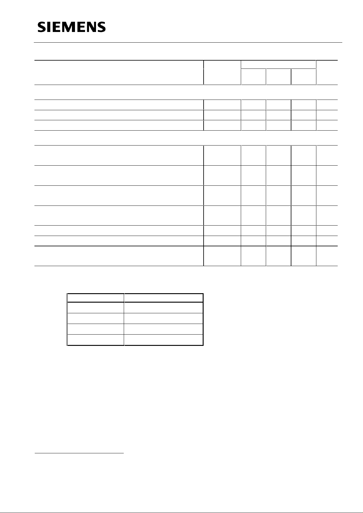
Electrical Characteristics
Parameter and Conditions Symbol Values Unit
VS = 4.8 to 18 V ; Tj = – 40 °C to + 150 °C
(unless otherwise specified)
5. Standby Input (STBY)
Input low voltage
Input high voltage
Input current V
STBY
= 18 V
6. Diagnostic Functions
Open load detection voltage VS ≥ 6.5 V
V
= X, VIN = L, VDC = 0
ENA
4
Open load compare voltage VS ≥ 6.5 V
V
= X, VIN = L, 18V ≥ V
ENA
DSC
≥ V
DS(OL)
4
Open load detection current channel 1,2 VS ≥ 6.5 V
V
= X, VIN = H
ENA
Open load detection current channel 3,4 VS ≥ 6.5 V
V
= X, VIN = H
ENA
Overload threshold current channel 1,2 VS ≥ 6.5 V
Overload threshold current channel 3,4 VS ≥ 6.5 V
Overtemperature shutdown threshold
5
Hysteresis
V
STBY
V
STBY
I
STBY
V
DS(OL)
V
DS(OL)C
I
D(OL) 1,2
I
D(OL) 3,4
I
D(lim) 1,2
I
D(lim) 3,4
T
th
T
hys
min typ max
01V
3.5 V
S
300 µA
0.52*V
V
S
-1.5 V
DSC
0.57*V
-1.0 V
DSC
S
160 480 mA
160 480 mA
5 7.5 A
35 A
170
200 °C
10
V
V
K
Table 1:
Channel Compared with Channel
V
V
V
V
4
V
is the output voltage of the corresponding channel, paired for open load detection Corresponding outputs
DSC
are channel 1 and 4, channel 2 and 3 (see table 1).
5
This parameter will not be tested but assured by design
14
DS(OL)
23
DS(OL)
32
DS(OL)
41
DS(OL)
Semiconductor Group Page 1998-02-04
6
Page 7
Application Description
This IC is especially designed to drive inductive loads (relays, electromagnetic valves).
Integrated clamp-diodes limit the output voltage when inductive loads are discharged.
Four open-drain logic outputs indicate the status of the integrated ciruit. The following conditions are
monitored and signalled:
- overloading of output (also shorted load to supply) in active mode
- open and shorted load to ground in active and inactive mode
- overtemperature
TLE 5226 G
Circuit Description
Input Circuits
The control and enable inputs, both active high, consist of schmitt triggers with hysteresis. All inputs
are connected with pull-down current sources. Not connected inputs are interpreted as LOW.
In standby mode (STBY = LOW ) the current consumption is greatly reduced. The circuit is active
when STBY = HIGH.
If the standby function is not used, it is allowed to connect the standby pin directly to V
Switching Stages
The four power outputs consist of DMOS-power transistors with open drains. The output stages are
shorted loads protected throughout the operating range. Integrated clamp-diodes limit voltage
overshoots produced when inductive loads are demagnetized.
Parallel to the DMOS transistors there are internal pull down resistors. They are provided to detect an
open load condition in the off state. They will be disconnected in the standby mode.
Protective Circuits
The outputs are protected against current overload and overtemperature.
There is no protection against reverse polarity of the supply voltage.
.
S
Error Detection
The status outputs indicate the switching state under nor mal conditions (LOW = off ; HIGH = on). If an
error occurs, the logic level of the status output is inverted, as listed in the diagnostic table below.
The state of the error detection circuits is directly dependent on the input status.
If current overload or overtemperat ure
the output is shutdown. The reset is done by switching off the corresponding control input.
Semiconductor Group Page 1998-02-04
occurs, the error condition is stored into an internal regist er and
7
Page 8
Open load is detected for all f our channels in on and off mode. In the on mode the load curr ent is monitored. If it drops below the specified threshold value, then an open load condition is detected.
In the off mode, the ouput voltage is monitored.
An open load condition is detected when the output voltage of a given channel is below 55 % of the
supply voltage V
condition with a fixed offset of typ. 1.25 V to recognize GND bypasses. To suppress fault diagnosis
during the flyback phase of the compared output, the diagnostic circuit includes a latch function.
Reset of this latch is done at end of the flyback phase, additionally it can be reseted by a low signal on
the enable input or a high signal of the input line.
See block diagramm of open load detection on page 3.
S. Also the output voltages of two outputs are compaired against each other in off
TLE 5226 G
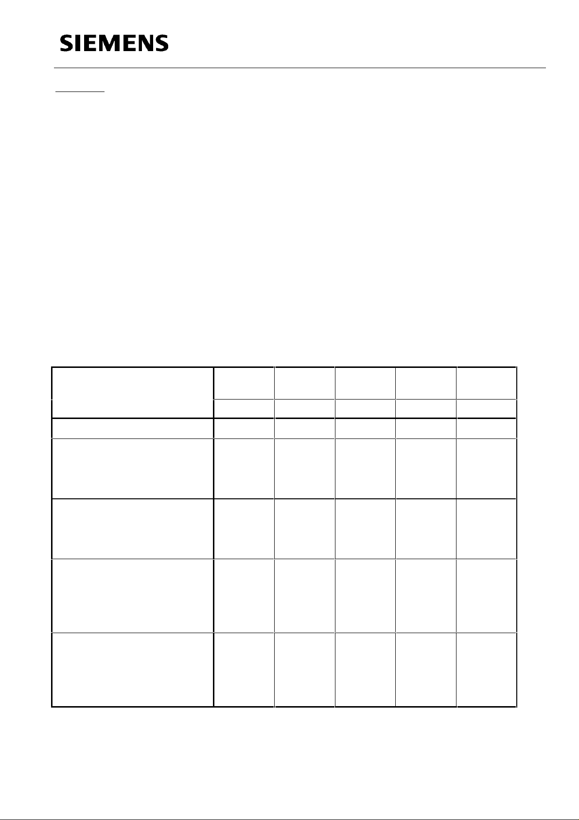
Diagnostic Table
In general the status follows the input signal in normal operating conditions.
If any error is detected the status is inverted.
Operating Condition
Standby
Input
Enable
Input
Control
Input
Power
Output
Status
Output
STBY ENA IN OUT ST
Standby L X X OFF H
Normal function H
H
H
H
Open load or short to ground H
H
H
H
Overload or short to supply
latched overload
H
H
H
H
H
H
H
H
H
L
L
L
L
L
H
H
H
H
H
H
H
L
OFF
OFF
L
L
L
OFF
ON
OFF
OFF
OFF
H
H
H
H
ON
OFF
OFF
OFF
H
L
L
L
L
L
L
reset latch
Overtemperature
latched overtemperature
reset latch
Semiconductor Group Page 1998-02-04
H
H
H
H
H
X
H
H
X
H → L
H
H
L
H
H → L
8
OFF
OFF
OFF
OFF
OFF
L
L
L
H
L
Page 9
TLE 5226 G
Diagnostic (continued)
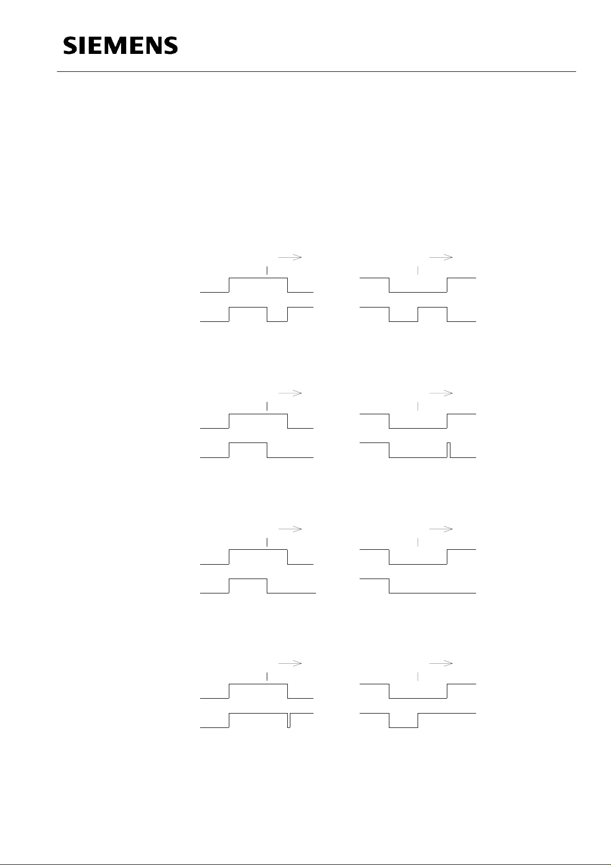
The following diagrams show the dynamical behaviour of the status output in case of different
errors.
The symbol F defines the moment of failure occurence.
Output open load or short circuit to GND
F F
IN
ST
Output overload
IN
ST
Overtemperature of the chip
IN
ST
Load Bypass
F F
F F
F F
IN
ST
Semiconductor Group Page 1998-02-04
9
Page 10
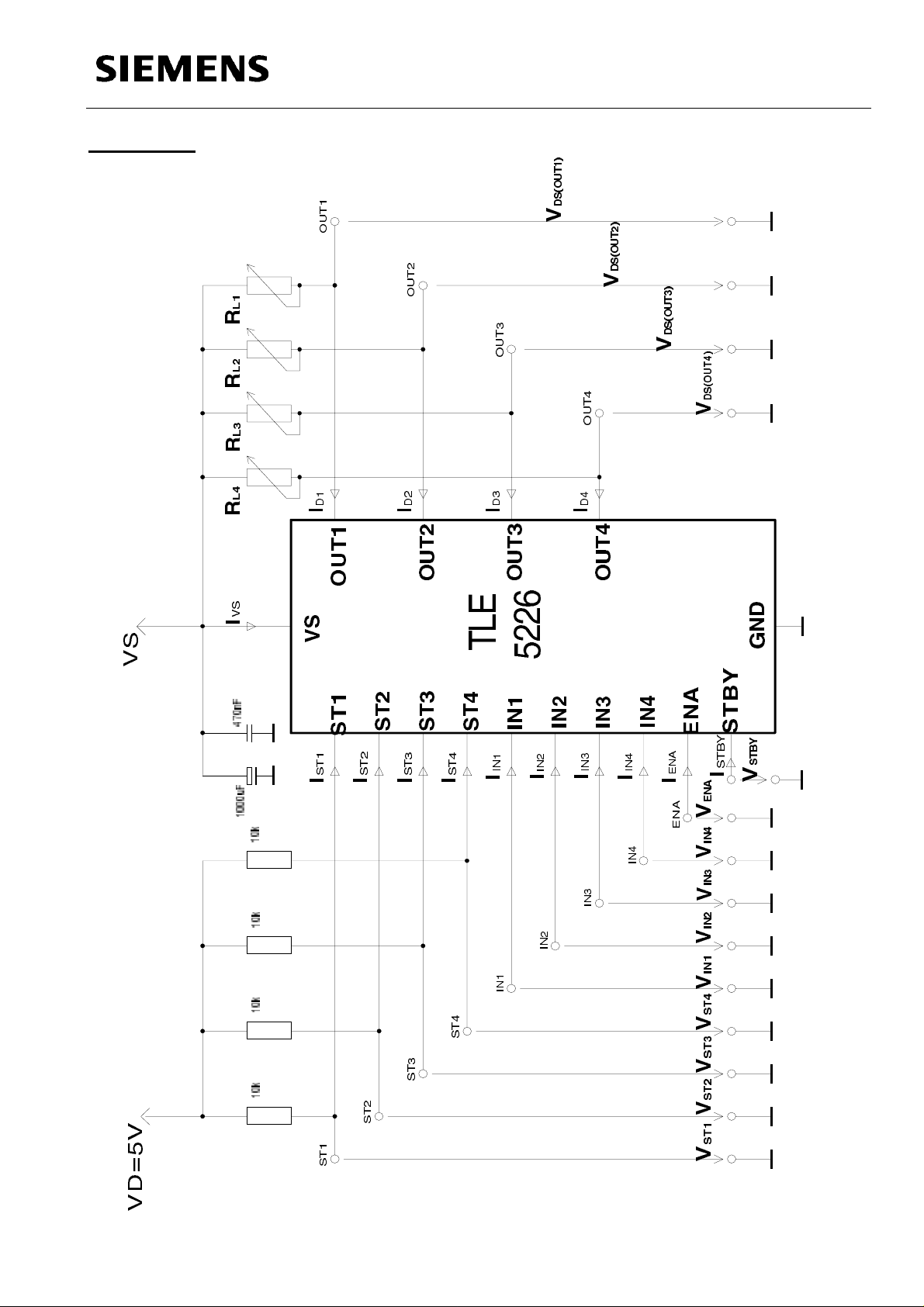
Test Ciruit
TLE 5226 G
Semiconductor Group Page 1998-02-04
10
Page 11
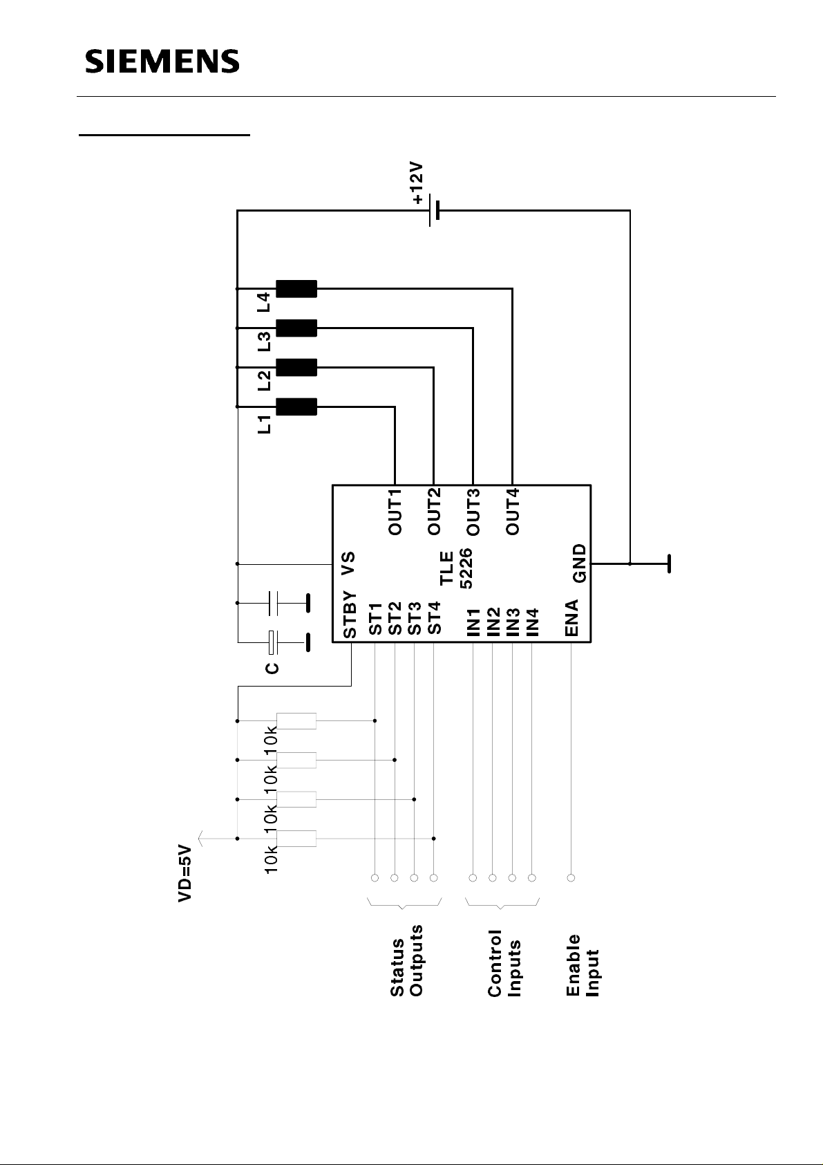
Application Circuit
TLE 5226 G
The blocking capacitor C is recommended to avoid critical negative voltage spikes on VS in case of
battery interruption during OFF-commutation.
Semiconductor Group Page 1998-02-04
11
Page 12
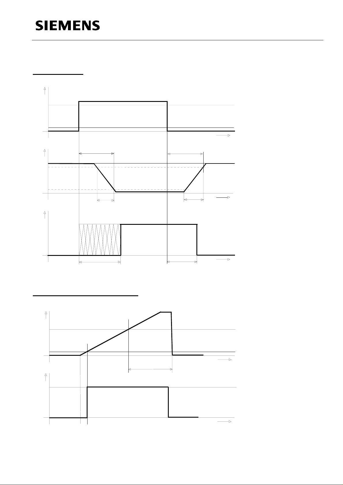
Output Slope
V
IN
V
INH
V
INL
TLE 5226 G
Timing Diagrams
t
t
V
DS
V
S
85%
15%
V
ST
on
t
t
5
fall
Overload Switch OFF Delay
I
D
t
t
off
4
t
t
rise
t
I
D(lim)
I
D(OL)
t
dso
V
ST
Semiconductor Group Page 1998-02-04
12
t
t
Page 13
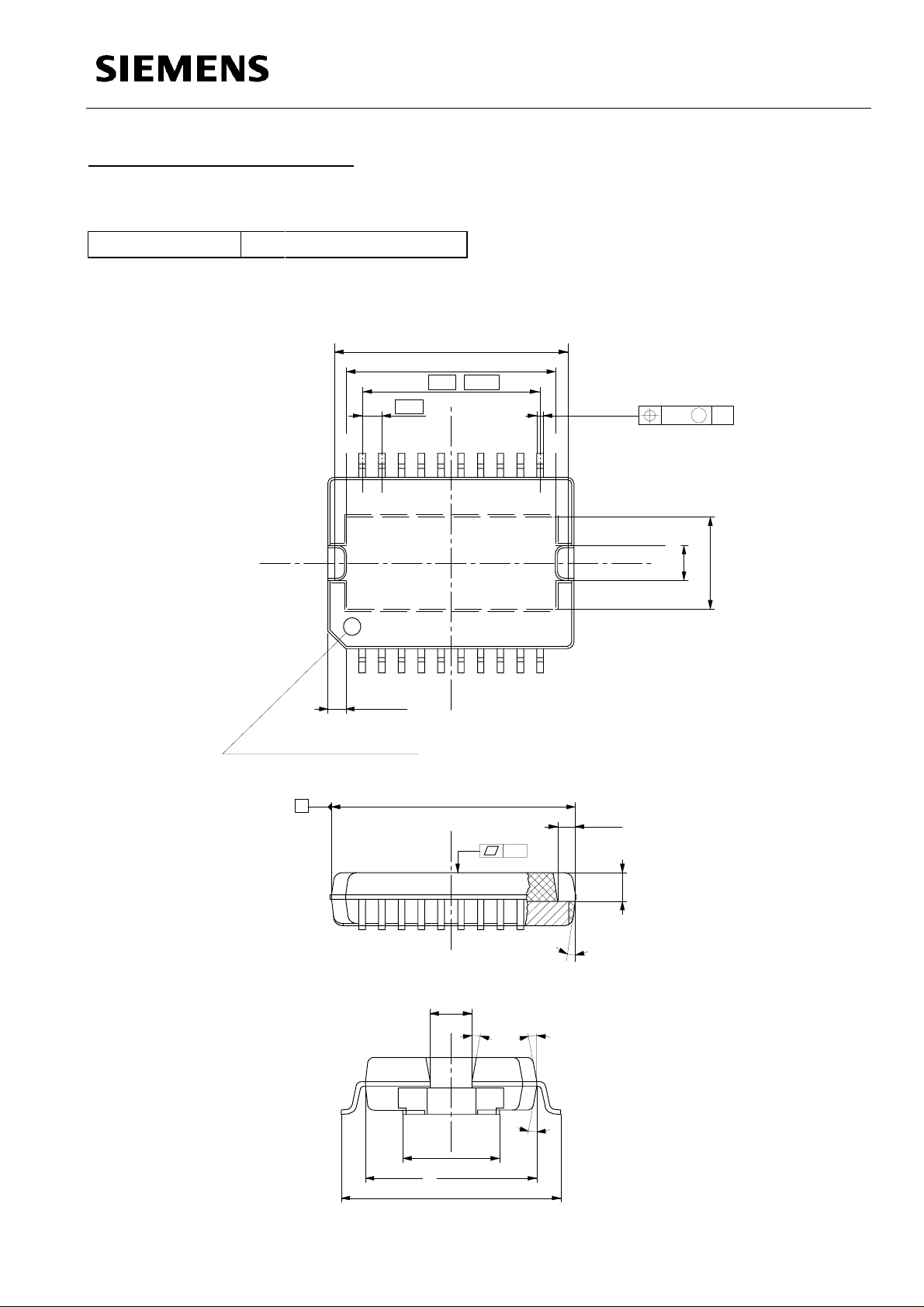
Package and ordering code
all dimensions in mm
TLE 5226 G
P - DSO - 20 - 10
Ordering code
Q67006-A9207
9 x =11.431.27
1.27
15.74
13.7
-0.2
+/- 0.1
+0.13
0.4
0.25 A
M
1120
+/-0.1
+/-0.1
3.2
5.9
110
1 x 45°
PIN 1 INDEX MARKING
A
15.9
+/-0.15
2.8
0.1
8° 8°
8°
1.2
-0.3
1.3
6.3
+/-0.15
11
+/-0.3
14.2
Semiconductor Group Page 1998-02-04
8°
1)
13
 Loading...