

TLE2301
EXCALIBUR 3-STATE-OUTPUT WIDE-BANDWIDTH
POWER OPERATIONAL AMPLIFIER
SLOS131 – DECEMBER 1993
D
High Output Drive Capability...1 A Min
D
3-State Outputs
D
High Gain-Bandwidth Product
8 MHz Typ
D
Low Total Harmonic Distortion
<0.08% Typ
D
High Slew Rate...12 V/µs Typ
D
Class AB Output Stage
D
Thermal Shutdown
D
Mains-Line Driver Circuit Application
Included
description
The TLE2301 is a power operational amplifier that
can deliver an output current of 1 A at high
frequencies with very low total harmonic
distortion. The device has an integral 3-state
mode to drive the output stage into a
high-impedance state and also to reduce the
supply current to less than 3.5 mA.
The combination of high output current and
3-state outputs makes the TLE2301 ideal for
implementing the signalling transformer driver in
mains-based telemetering modems. This
combination of features also makes the device
well suited for other high-current applications
(e.g., motor drivers and audio circuits).
Using the Texas Instruments established
Excalibur process, the TLE2301 is able to achieve
slew rates in excess of 12 V/µs and a gainbandwidth product of 8 MHz. The TLE2301 uses
a 16-pin NE power package to provide better
power handling capabilities than standard dual-inline packages.
NE PACKAGE
(TOP VIEW)
COMP2
V
OUT1
V
V
OUT2
V
TRS2
Terminals 4, 5, 12 and 13 are
connected to the lead frame.
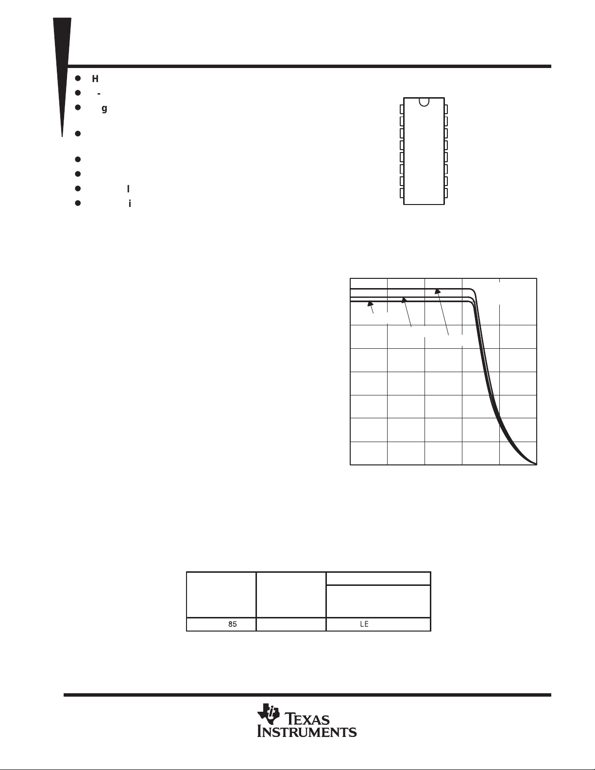
MAXIMUM PEAK-TO-PEAK OUTPUT VOLTAGE
8
7
RL = 4.3 Ω
6
5
4
3
2
– Maximum Peak-to-Peak Output Voltage – V
1
O(PP)
V
0
100 1 k 10 k 100 k
CC+
CC–
CC–
CC+
1
2
3
4
5
6
7
8
FREQUENCY
RL = 8.1 Ω
f – Frequency – Hz
COMP1
16
V
15
CC–
1N+
14
V
13
CC–
V
12
CC–
11
IN–
10
V
CC–
9
TRS1
vs
RL = 20 Ω
V
CC±
TA = 25°C
1 M 10 M
Figure 1
= ±5 V
The TLE2301 is characterized for operation over
the industrial temperature range of –40°C to
85°C.
T
A
–40°C to 85°C 10 mV TLE2301INE
PRODUCTION DATA information is current as of publication date.
Products conform to specifications per the terms of Texas Instruments
standard warranty. Production processing does not necessarily include
testing of all parameters.
POST OFFICE BOX 655303 • DALLAS, TEXAS 75265
AVAILABLE OPTION
VIOmax AT 25°C
PACKAGE
THERMALLY-ENHANCED
PLASTIC DIP
(NE)
Copyright 1993, Texas Instruments Incorporated
1
TLE2301
EXCALIBUR 3-STATE-OUTPUT WIDE-BANDWIDTH
POWER OPERATIONAL AMPLIFIER
SLOS131 – DECEMBER 1993
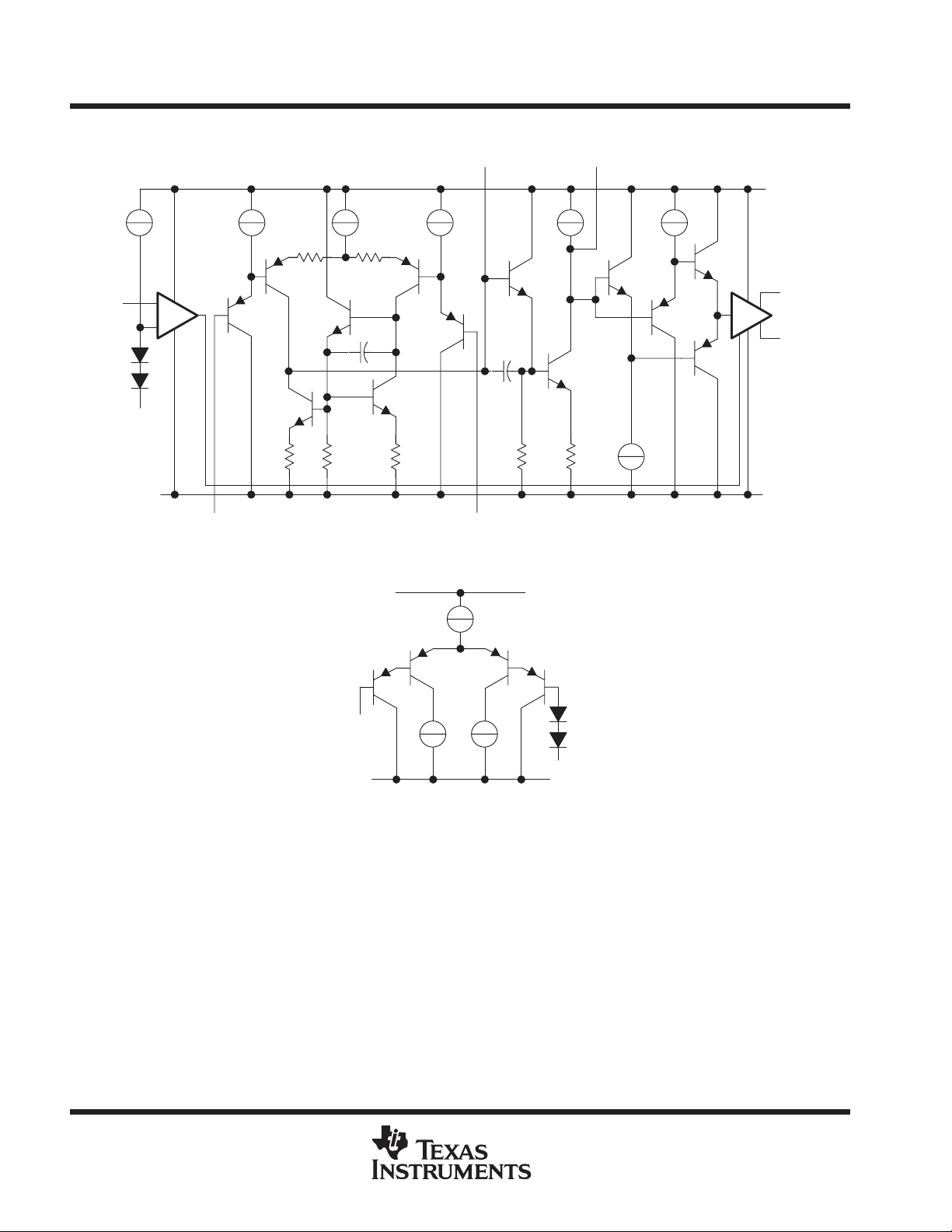
equivalent schematic (entire device)
COMP1 COMP2
V
CC+
TRS1
+
_
TRS2
IN+ IN–
equivalent schematic (TRS1 and TRS2 inputs)
V
CC+
TRS1
V
CC–
OUT1
OUT2
V
CC–
2
POST OFFICE BOX 655303 • DALLAS, TEXAS 75265
TRS2
DESCRIPTION
gg
(yµg) g yg g
TLE2301
EXCALIBUR 3-STATE-OUTPUT WIDE-BANDWIDTH
POWER OPERATIONAL AMPLIFIER
SLOS131 – DECEMBER 1993
Terminal Functions
TERMINAL
NAME NO.
COMP1 16 COMP1 and COMP2 are compensation network terminals
COMP2 1
IN+ 14 Noninverting input
IN– 11 Inverting input
OUT1 3 Two low-distortion class-AB output stages. Each is capable of sourcing more than 500 mA. OUT1 and OUT2 should be
OUT2 6
TRS1
TRS2
V
V
V
CC–
CC–
CC+
10, 15 High-impedance V
12, 13
connected together for all applications.
98TRS1 and TRS2 are 3-state input terminals. TRS2 should be connected to the ground of the circuit generating the 3-state
command (normally µP ground). The TLE2301 is brought into 3-state mode by raising TRS1 2 V above TRS2. Placing the
TLE2301 in a 3-state mode reduces the supply current to below 2.2 mA (typ). Normal operation resumes by bringing TRS1
to within 0.8 V of TRS2. The 3-state function can be disabled by connecting both TRS1 and TRS2 to V
input terminals. Although these do not carry any of the device’s supply current, they increase the
stability of the device and should be connected to the negative supply terminal (V
4, 5,
Negative supply terminals and substrate. As with all NE packages, the substrate is directly connected to the lead frame.
The result is that the junction-to-ambient thermal impedance (Z
terminals to the copper area of the printed-circuit board (PCB).
2, 7 Positive supply terminals. Both terminals should be connected to the positive voltage supply.
CC–
).
CC–
) is greatly reduced by soldering the negative supply
θJA
CC–
.
POST OFFICE BOX 655303 • DALLAS, TEXAS 75265
3
TLE2301
EXCALIBUR 3-STATE-OUTPUT WIDE-BANDWIDTH
POWER OPERATIONAL AMPLIFIER
SLOS131 – DECEMBER 1993
absolute maximum ratings over operating free-air temperature range (unless otherwise noted)
Supply voltage, V
Supply voltage, V
Differential input voltage, V
Duration of short-circuit current at (or below) 25°C (see Note 3) unlimited. . . . . . . . . . . . . . . . . . . . . . . . . . . . . .
Continuous total dissipation at (or below) 25°C free-air temperature (see Notes 4 and 5) 2075 mW. . . . . . .
Continuous total dissipation at 85°C case temperature (see Note 5) 4640 mW. . . . . . . . . . . . . . . . . . . . . . . . .
Operating free-air temperature range, T
Operating case or virtual junction temperature range –40°C to 150°C. . . . . . . . . . . . . . . . . . . . . . . . . . . . . . . . .
Storage temperature range –65°C to 150°C. . . . . . . . . . . . . . . . . . . . . . . . . . . . . . . . . . . . . . . . . . . . . . . . . . . . . . . .
†
Stresses beyond those listed under “absolute maximum ratings” may cause permanent damage to the device. These are stress ratings only, and
functional operation of the device at these or any other conditions beyond those indicated under “recommended operating conditions” is not
implied. Exposure to absolute-maximum-rated conditions for extended periods may affect device reliability.
NOTES: 1. All voltage values, except differential voltages, are with respect to the midpoint between V
2. Differential voltages are at IN+ with respect to IN–.
3. The outputs when connected together may be shorted to either supply. T emperature and/or supply voltages must be limited to ensure
that the maximum dissipation rating is not exceeded.
4. For operation above 25°C free-air temperature, derate linearly at the rate of 16.56 mW/°C.
5. For operation above 25°C case temperature, derate linearly at the rate of 71.4 mW/°C. To avoid exceeding the design maximum
virtual junction temperature, these ratings should not be exceeded. Due to variations in individual device electrical characteristics
and thermal resistance, the built-in thermal overload protection may be activated at power levels slightly above or below the rated
dissipation.
FREE-AIR TEMPERATURE
DISSIPATION DERATING CURVE
2.5
Derating Factor = 16.56 mW/°C
Z
= 60.4°C/W
θJC
2
(see Note 1) 22 V. . . . . . . . . . . . . . . . . . . . . . . . . . . . . . . . . . . . . . . . . . . . . . . . . . . . . . . . . . .
CC+
(see Note 1) –22 V. . . . . . . . . . . . . . . . . . . . . . . . . . . . . . . . . . . . . . . . . . . . . . . . . . . . . . . . . .
CC–
(see Note 2) ±44 V. . . . . . . . . . . . . . . . . . . . . . . . . . . . . . . . . . . . . . . . . . . . . . . . . . .
ID
–40°C to 85°C. . . . . . . . . . . . . . . . . . . . . . . . . . . . . . . . . . . . . . . . . . . .
A
CC+
and V
CC–
.
CASE TEMPERATURE
DISSIPATION DERATING CURVE
10
8
†
1.5
1
0.5
– Total Continuous Power Dissipation – W
D
P
0
25 40 55 70
TA – Free-Air Temperature – ° C
85
6
4
2
– Total Continuous Power Dissipation – W
D
P
Derating Factor = 71.4 mW/°C
Z
= 14°C/W
θJC
0
0 25 50 75 100
TC – Case Temperature – °C
4
POST OFFICE BOX 655303 • DALLAS, TEXAS 75265
Common-mode input voltage, V
VIOInput offset voltage
O
,
IC
,
mV
IIBInput bias current
O
,
IC
,
nA
4
ICR
gg
S
g
V
Maximum positive peak output voltage swing
R
See Note 6
V
V
Maximum negative peak output voltage swing
R
See Note 6
V
AVDLarge-signal differential voltage amplification
O
,
IC
,
dB
roOutput resistance (see Note 7)
25°C
CMRR
Common-mode rejection ratio
IC ICR
,
O
,
25°C6588
dB
k
Suppl
oltage rejection ratio (∆V
/∆VIO)
CC±
,
25°C70100
dB
IIHEnable input current, high
V
3-state mode
A
IILEnable input current, lo
V
V
A
V
No load
ICCSupply current
mA
O
TLE2301
EXCALIBUR 3-STATE-OUTPUT WIDE-BANDWIDTH
POWER OPERATIONAL AMPLIFIER
SLOS131 – DECEMBER 1993
recommended operating conditions
MIN MAX UNIT
Supply voltage, V
High-level 3-state enable voltage, V
Low-level 3-state enable voltage, V
Continuous output current 1 A
Operating free-air temperature, T
CC±
p
V
= ±5 V –4 1.6 V
IC
IH
IL
A
CC±
V
= ±15 V –14 11.8 V
CC±
±4.5 ±20 V
2 V
0.8 V
–40 85 °C
electrical characteristics at specified free-air temperature, V
otherwise noted) (see Figure 5)
PARAMETER TEST CONDITIONS
V
p
p
V
r
I
OS
†
Full range is –40°C to 85°C.
NOTES: 6. OUT1 and OUT2 are connected together for all tests.
Common-mode input voltage range RS = 50 Ω Full range
ICR
p
OM+
OM–
Differential input resistance 25°C 1 MΩ
i
p
pp
SVR
y-v
p
p
Short-circuit output current (see Note 8)
pp
7. TRS1 voltage is measured with respect to TRS2 potential.
8. Pulse testing techniques are used to maintain the junction temperature as close to the ambient temperature as possible. Thermal
effects must be taken into account separately (tp = pulse duration time).
p
p
p
p
p
CC±
w
= 0, V
RS = 50 Ω
V
= 0, V
RS = 50 Ω
= 20 Ω,
L
= 20 Ω,
L
V
= ±2 V, V
RL = 20 Ω
TRS1 = 0.8 V
TRS1 = 2 V, 3-state mode
V
= V
RS = 50 Ω
V
VIC = 0, No load
= 2 V,
I
= 0.8
I
VO = 0, tp ≤ 50 µs
= 0,
O
VO = 0, No load,
3-state mode
min, V
= ±4.5 V to ±20 V,
= 0,
= 0,
= 0,
= 0,
= ±5 V, CC = 15 pF (unless
CC±
†
T
A
25°C 0.4 7
Full range 10
25°C 283 450
Full range 500
25°C 3.3 3.5
Full range 3.2
25°C –3.2 –3.4
Full range –3.1
25°C 65 87
Full range 60
°
°
°
25°C 0.01 0.5
Full range 0.5
25°C 0.01 0.5
Full range 0.5
25°C 1 1.8 A
25°C 10 21
Full range 25
25°C 1.73 2.7
Full range 3.5
MIN TYP MAX
–4
to
1.6
1 Ω
100 kΩ
UNIT
V
µ
µ
POST OFFICE BOX 655303 • DALLAS, TEXAS 75265
5
TLE2301
VIOInput offset voltage
O
,
IC
,
mV
IIBInput bias current
O
,
IC
,
nA
14
ICR
gg
S
g
V
Maximum positive peak output voltage swing
R
See Note 6
V
V
Maximum negative peak output voltage swing
R
20 Ω
See Note 6
V
AVDLarge-signal differential voltage amplification
O
,
IC
,
dB
roOutput resistance (see Note 7)
25°C
k
Suppl
oltage rejection ratio (∆V
/∆VIO)
CC±
,
25°C70100
dB
IIHEnable input current, high
V
3-state mode
A
IILEnable input current, lo
V
V
A
V
No load
ICCSupply current
mA
O
EXCALIBUR 3-STATE-OUTPUT WIDE-BANDWIDTH
POWER OPERATIONAL AMPLIFIER
SLOS131 – DECEMBER 1993
electrical characteristics at specified free-air temperature, V
otherwise noted) (see Figure 5)
PARAMETER TEST CONDITIONS
V
p
p
V
r
i
CMRR Common-mode rejection ratio
I
OS
†
Full range is –40°C to 85°C.
NOTES: 6. OUT1 and OUT2 are connected together for all tests.
Common-mode input voltage range RS = 50 Ω Full range
ICR
p
OM+
OM–
Differential input resistance 25°C 1 MΩ
p
pp
SVR
y-v
p
p
Short-circuit output current (see Note 8)
pp
7. TRS1 voltage is measured with respect to TRS2 potential.
8. Pulse testing techniques are used to maintain the junction temperature as close to the ambient temperature as possible. Thermal
effects must be taken into account separately (tp = pulse duration time).
p
p
p
p
p
CC±
w
= 0, V
RS = 50 Ω
V
= 0, V
RS = 50 Ω
= 20 Ω,
L
=
L
V
= ±6 V, V
RL = 20 Ω
TRS1 = 0.8 V
TRS1 = 2 V, 3-state mode
VIC = V
RS = 50 Ω
V
VIC = 0, No load
= 2 V,
I
= 0.8
I
VO = 0, tp ≤ 50 µs
= 0,
O
VO = 0, No load,
3-state mode
,
min,
ICR
= ±4.5 V to ±20 V,
= 0,
= 0,
= 0,
VO = 0,
= ± 15 V, CC = 15 pF (unless
CC ±
†
T
A
25°C 0.3 10
Full range 15
25°C 260 450
Full range 500
25°C 13 13.5
Full range 13
25°C –12.6 –13
Full range –12.5
25°C 70 102
Full range 65
°
25°C 70 97 dB
°
25°C 0.01 0.5
Full range 0.5
25°C 0.01 0.5
Full range 0.5
25°C 1 3 A
25°C 11 25
Full range 30
25°C 2.2 3.5
Full range 5
MIN TYP MAX
–14
to
11.8
1 Ω
100 kΩ
UNIT
V
µ
µ
6
POST OFFICE BOX 655303 • DALLAS, TEXAS 75265
tsSettling time (see Figure 1)
L
,
L
,
0.7µs
tsSettling time (see Figure 1)
L
,
L
,
1.8µs
TLE2301
EXCALIBUR 3-STATE-OUTPUT WIDE-BANDWIDTH
POWER OPERATIONAL AMPLIFIER
SLOS131 – DECEMBER 1993
operating characteristics at specified free-air temperature, V
(unless otherwise noted) (see Figure 5)
PARAMETER TEST CONDITIONS MIN TYP MAX
SR Slew rate at unity gain (see Figure 1)
V
n
THD Total harmonic distortion
B
1
φ
m
Equivalent input noise voltage (see Figure 2) RS = 50 Ω, f = 1 kHz 44
Unity-gain bandwidth (see Figure 3) RL = 20 Ω, CL = 100 pF 8 MHz
Phase margin at unity gain (see Figure 3) RL = 20 Ω, CL = 100 pF 30°
VO = ±1.5 V ,
CL = 100 pF
R
= 20 Ω, C
3-V step to 30 mV (1%)
VO = 1 V
RL = 20 Ω,
rms
,
operating characteristics at specified free-air temperature, V
(unless otherwise noted) (see Figure 5)
PARAMETER TEST CONDITIONS MIN TYP MAX
SR Slew rate at unity gain (see Figure 1)
V
n
THD Total harmonic distortion
B
1
φ
m
Equivalent input noise voltage (see Figure 2) RS = 50 Ω, f = 1 kHz 44
Unity-gain bandwidth (see Figure 3) RL = 20 Ω, CL = 100 pF 8 MHz
Phase margin at unity gain (see Figure 3) RL = 20 Ω, CL = 100 pF 35°
VO = ±10 V,
CL = 100 pF
R
= 20 Ω, C
20-V step to 200 mV (1%)
VO = 2 V
RL = 20 Ω,
rms
,
= ± 5 V, CC = 15 pF, TA = 25°C
CC ±
RL = 20 Ω,
= 100 pF,
f = 50 kHz,
CL = 100 pF
= ± 15 V, CC = 15 pF, TA = 25°C
CC ±
RL = 20 Ω,
= 100 pF,
f = 50 kHz,
CL = 100 pF
9 12 V/µs
0.04%
9 14 V/µs
0.08%
UNIT
nV/√Hz
UNIT
nV/√Hz
POST OFFICE BOX 655303 • DALLAS, TEXAS 75265
7

TLE2301
EXCALIBUR 3-STATE-OUTPUT WIDE-BANDWIDTH
POWER OPERATIONAL AMPLIFIER
SLOS131 – DECEMBER 1993
PARAMETER MEASUREMENT INFORMATION
V
CC+
_
V
+
V
I
V
CC–
C
(see Note A)
NOTE A: CL includes the fixture capacitance.
L
O
R
L
Figure 2. Slew-Rate Test Circuit
10 kΩ
V
CC+
V
I
NOTE A: CL includes the fixture capacitance.
_
+
V
CC–
C
(see Note A)
V
O
R
L
L
5 kΩ
V
CC+
_
V
+
V
CC–
50 Ω50 Ω
O
Figure 3. Noise-Voltage Test Circuit
R
2
V
R
V
I–
V
I+
1
R
3
COMP1 COMP1
_
+
V
15 pF
CC+
CC–
C
c
V
O
Figure 4. Gain-Bandwidth and
Figure 5. Compensation Configuration
Phase-Margin Test Circuit
typical values
Typical values presented in this data sheet represent the median (50% point) of the device parametric
performance.
8
POST OFFICE BOX 655303 • DALLAS, TEXAS 75265

AVDDifferential voltage amplification
VOMMaximum peak output voltage
ICCSupply current
Pulse response
TLE2301
EXCALIBUR 3-STATE-OUTPUT WIDE-BANDWIDTH
POWER OPERATIONAL AMPLIFIER
SLOS131 – DECEMBER 1993
TYPICAL CHARACTERISTICS
Table of Graphs
FIGURE
I
IB
I
IO
VO(
Z
θJA
z
o
Input bias current vs Free-air temperature 6, 7
Input offset current vs Free-air temperature 6, 7
p
Maximum peak-to-peak output voltage vs Frequency 10, 11
PP)
p
p
Transient junction-to-ambient thermal impedance vs Time 15
pp
p
Output impedance vs Frequency 22, 23
vs Frequency 8
vs Free-air temperature 9
vs Output current 12, 13
vs Supply voltage 14
vs Supply voltage 16
vs Free-air temperature 17
Small signal
Large signal
18, 19
20, 21
INPUT BIAS CURRENT AND
INPUT OFFSET CURRENT
vs
FREE-AIR TEMPERATURE
1000
V
= ±15 V
CC±
VIC = 0
I
100
10
IO
I
1
IB
IIB and IIO – Input Bias and Input Offset Currents – nA
I
–50 –25 0 25 50 75 100
TA – Free-Air Temperature – ° C
IB
I
IO
Figure 6
INPUT BIAS CURRENT AND
INPUT OFFSET CURRENT
vs
FREE-AIR TEMPERATURE
1000
V
= ±5 V
CC±
VIC = 0
I
100
10
1
IO
I
0.1
IB
IIB and IIO – Input Bias and Input Offset Currents – nA
I
–50 –25 0 25 50 75 100
TA – Free-Air Temperature – ° C
IB
I
IO
Figure 7
POST OFFICE BOX 655303 • DALLAS, TEXAS 75265
9

TLE2301
EXCALIBUR 3-STATE-OUTPUT WIDE-BANDWIDTH
POWER OPERATIONAL AMPLIFIER
SLOS131 – DECEMBER 1993
TYPICAL CHARACTERISTICS
DIFFERENTIAL VOLTAGE AMPLIFICATION
120
100
80
60
40
20
– Differential Voltage Amplification – dB
0
VD
A
–20
10 100 1 k 10 k
vs
FREQUENCY
100 k 1 M 10 M
f – Frequency – Hz
Figure 8
V
= ±15 V
CC±
RL = 20 Ω
CC = 100 pF
TA = 25°C
20°
40°
60°
80°
100°
120°
140°
160°
DIFFERENTIAL VOLTAGE AMPLIFICATION
vs
FREE-AIR TEMPERATURE
110
RL = 20 Ω
100
90
80
70
– Differential Voltage Amplification – dB
VD
A
60
–50 –25 0 25 50 75 100
V
= ±15 V
CC±
V
= ±5 V
CC±
TA – Free-Air Temperature – ° C
Figure 9
MAXIMUM PEAK-TO-PEAK OUTPUT VOLTAGE
vs
FREQUENCY
30
RL = 20 Ω
25
20
15
10
– Maximum Peak-to-Peak Output Voltage – V
O(PP)
V
RL = 8.1 Ω
5
0
100 1 k 10 k 100 k
f – Frequency – Hz
Figure 10
V
= ±15 V
CC±
TA = 25°C
1 M 10 M
MAXIMUM PEAK-TO-PEAK OUTPUT VOLTAGE
8
7
RL = 4.3 Ω
6
5
4
3
2
– Maximum Peak-to-Peak Output Voltage – V
1
O(PP)
V
0
100 1 k 10 k 100 k
RL = 8.1 Ω
f – Frequency – Hz
Figure 11
vs
FREQUENCY
RL = 20 Ω
V
= ±5 V
CC±
TA = 25°C
1 M 10 M
10
POST OFFICE BOX 655303 • DALLAS, TEXAS 75265

TLE2301
EXCALIBUR 3-STATE-OUTPUT WIDE-BANDWIDTH
POWER OPERATIONAL AMPLIFIER
SLOS131 – DECEMBER 1993
TYPICAL CHARACTERISTICS
MAXIMUM POSITIVE PEAK OUTPUT VOLTAGE
vs
OUTPUT CURRENT
15
12.5
10
7.5
5
2.5
– Maximum Positive Peak Output Voltage – V
OM +
0
V
0 200 400 600
IO – Output Current – mA
TA = 25°C
V
CC±
V
CC±
Figure 12
= ±15 V
= ±5 V
800 1000
MAXIMUM NEGATIVE PEAK OUTPUT VOLTAGE
vs
OUTPUT CURRENT
– 15
– 12.5
– 10
– 7.5
– 5
– 2.5
– Maximum Negative Peak Output Voltage – V
OM –
0
V
0 200 400 600
IO – Output Current – mA
TA = 25°C
V
CC±
V
CC±
Figure 13
= ±15 V
= ±5 V
800 1000
MAXIMUM PEAK OUTPUT VOLTAGE
SUPPLY VOLTAGE
20
RL = 20 Ω
TA = 25°C
15
10
5
0
–5
–10
– Maximum Peak Output Voltage – V
OM
–15
V
–20
024681012
V
– Supply Voltage – V
CC±
Figure 14
vs
V
OM+
V
OM–
14 16 18 20
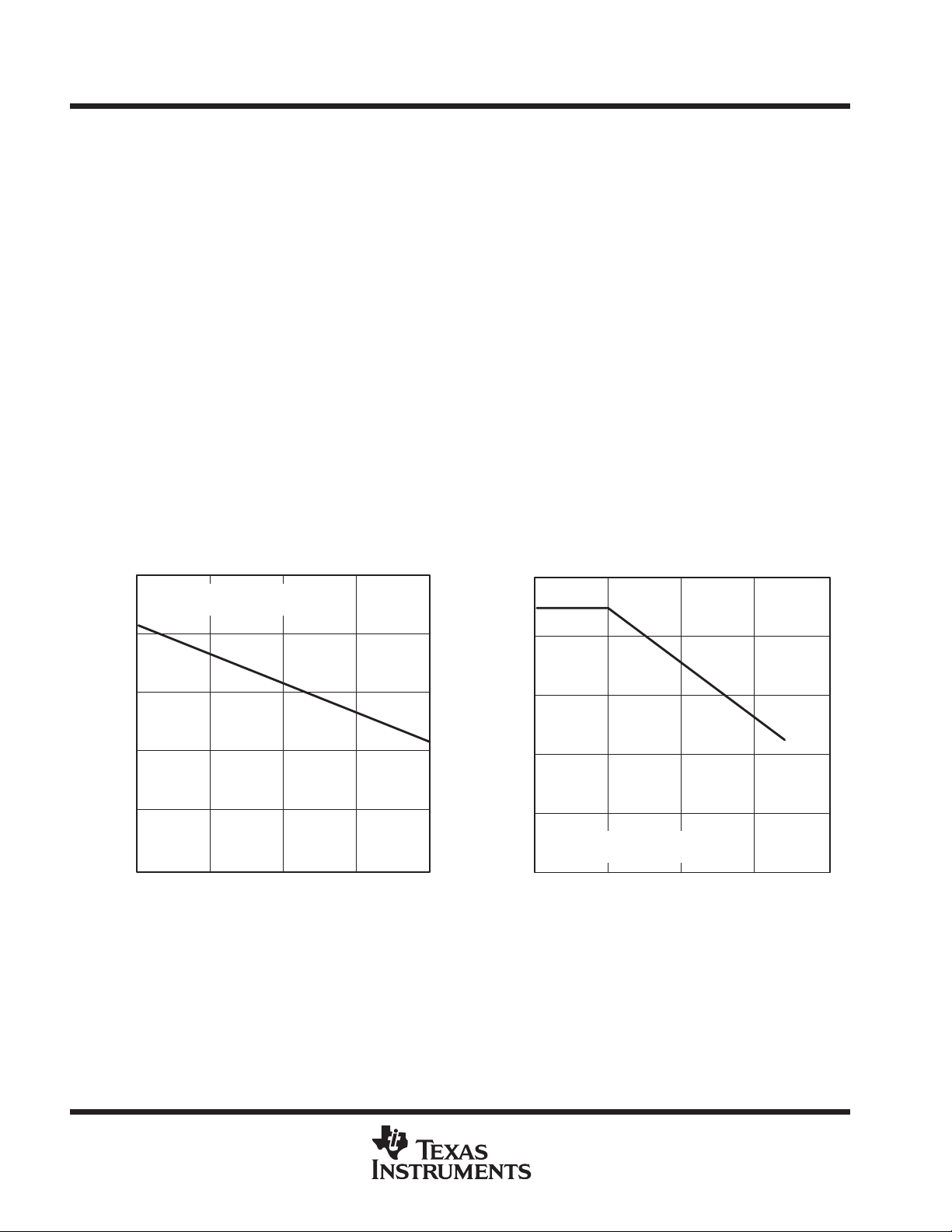
TRANSIENT JUNCTION-TO-AMBIENT
THERMAL IMPEDANCE
vs
ON TIME
100
d = 50%
d = 20%
°
10
d = 10%
d = 5%
d = 2%
1
– Transient Junction-to-Ambient
Thermal Impedance – C/mW
JAθ
Z
0.1
0.001 0.01 0.1 1 10 100 1000
Single Pulse
t – On Time – s
Figure 15
†
†
d = duty cycle
POST OFFICE BOX 655303 • DALLAS, TEXAS 75265
11

TLE2301
EXCALIBUR 3-STATE-OUTPUT WIDE-BANDWIDTH
POWER OPERATIONAL AMPLIFIER
SLOS131 – DECEMBER 1993
TYPICAL CHARACTERISTICS
SUPPLY CURRENT
SUPPLY VOLTAGE
10.8
VO = 0
No Load
10.7
TA = 25°C
10.6
10.5
10.4
10.3
10.2
– Supply Current – mA
CC
10.1
I
10
9.9
024681012
V
– Supply Voltage – V
CC±
Figure 16
vs
14 16 18 20
SUPPLY CURRENT
vs
FREE-AIR TEMPERATURE
10.8
VO = 0
No Load
10.6
V
= ±15 V
CC±
10.4
10.2
10
– Supply Current – mA
9.8
CC
I
9.6
9.4
–50 –25 0 25 50 75 100
TA – Free-Air Temperature – ° C
V
CC±
= ±5 V
Figure 17
VOLTAGE FOLLOWER
SMALL-SIGNAL
PULSE RESPONSE
15
10
5
0
– Output Voltage – V
–5
O
V
–10
–15
–2 0 2 4 6 8 10 12 14
V
= ±15 V
CC±
RL = 20 Ω
CL = 100 pF
TA = 25°C
t – Time – µs
Figure 18
VOLTAGE FOLLOWER
SMALL-SIGNAL
PULSE RESPONSE
150
100
50
0
– Output Voltage – mV
–50
O
V
–100
–150
–0.5 0 0.5 1 1.5 2 2.5
V
= ±5 V
CC±
RL = 20 Ω
CL = 100 pF
TA = 25°C
t – Time – µs
Figure 19
12
POST OFFICE BOX 655303 • DALLAS, TEXAS 75265

TLE2301
EXCALIBUR 3-STATE-OUTPUT WIDE-BANDWIDTH
POWER OPERATIONAL AMPLIFIER
SLOS131 – DECEMBER 1993
TYPICAL CHARACTERISTICS
VOLTAGE FOLLOWER
LARGE-SIGNAL
PULSE RESPONSE
150
V
CC±
100
50
0
– Output Voltage – mV
–50
O
V
–100
–150
–0.5 0 0.5 1 1.5 2 2.5
t – Time – µs
RL = 20 Ω
CL = 100 pF
TA = 25°C
Figure 20
= ±15 V
VOLTAGE FOLLOWER
LARGE-SIGNAL
PULSE RESPONSE
3
2
1
0
– Output Voltage – V
–1
O
V
–2
–3
–2 0 2 4 6 8 10 12 14
V
= ±5 V
CC±
RL = 20 Ω
CL = 100 pF
TA = 25°C
t – Time – µs
Figure 21
OUTPUT IMPEDANCE
vs
FREQUENCY
4
V
= ±15 V
CC±
TA = 25°C
3.5
3
Ω
2.5
2
1.5
– Output Impedance –
1
o
z
0.5
0
1 k
10 k 100 k 1 M 10 M
AVD = 100
AVD = 10
f – Frequency – Hz
Figure 22
AVD = 1
OUTPUT IMPEDANCE
vs
FREQUENCY
4
V
= ±5 V
CC±
TA = 25°C
3.5
Ω
3
AVD = 100
2.5
2
1.5
– Output Impedance –
o
1
z
0.5
0
1 k 10 k 100 k 1 M 10 M
AVD = 10
AVD = 1
f – Frequency – Hz
Figure 23
POST OFFICE BOX 655303 • DALLAS, TEXAS 75265
13

TLE2301
EXCALIBUR 3-STATE-OUTPUT WIDE-BANDWIDTH
POWER OPERATIONAL AMPLIFIER
SLOS131 – DECEMBER 1993
APPLICATION INFORMATION
circuit for mains-line driver over 40-kHz-to-90-kHz utility band
The following application is a circuit for
around the European standard (EN56065–1) describing utility and consumer applications. This example shows
a possible implementation for differential transmission on the mains line. This applications circuit is designed
around the requirements of a domestic electricity meter operating over a utility band of 40 kHz to 90 kHz. A
dual-rail power supply of ±5 V is used for this design example to limit device power dissipation. The same design
principles, however, can be applied to other applications.
frequency band
The frequency band for utility applications extends over an enormous range from 3 kHz to 95 kHz. In order to
have a coupling network that is economical and implemented with readily available components, this circuit is
designed for a subband from 40 kHz to 90 kHz.
This subband is sufficiently wide to support multichannel operation; i.e., 10 channels of 5 kHz width or more if
the channel widths are smaller. To avoid transmission spillover into the next band, a guard band of 5 kHz is
allowed. The upper frequency of this circuit is set to 90 kHz, and the lower frequency is chosen for an economical
coupling network and still has sufficient bandwidth to support multichannel operation.
output drive
The impedance of the mains network at these signalling frequencies is relatively low (<1 Ω to 30 Ω). This circuit
has been designed to drive a 4-Ω mains line over the 40-kHz-to-90-kHz bandwidth.
The signalling impedance of the mains network fluctuates as different loads are switched on during the day or
over a season, and it is influenced by many factors such as:
D
Localized loading from appliances connected to the mains supply near to the connection of the
communication equipment; e.g., heavy loads such as cookers and immersion heaters and reactive loads
such as EMC filters and power factor correctors
a mains-line driver over 40-kHz-to-90-kHz utility band
and is based
D
Distributed loading from consumers connected to the same mains cable, where their collective loading
reduces the mains signalling impedance during times of peak electricity consumption; e.g., meal times
D
Network parameters; e.g., transmission properties of cables and the impedance characteristics of
distribution transformers and other system elements
With such a diversity of factors, the signalling environment fluctuates enormously, irregularly, and can differ
greatly from one installation to another. The signalling system should be designed for reliable communications
over a wide range of mains impedances and signalling conditions. Consequently , the transmitter must be able
to drive sufficient signal into the mains network under these loading conditions.
The TLE2301 amplifier has 1-A output drive capability with short-circuit protection; hence, it adequately copes
with the high current demands required for implementing mains signalling systems.
3-state facility
When transmitting, the transmitter appears as a low-impedance signal source on the mains network. If
transmitters are left in the active mode whether transmitting or not and a large number of transmitters are
installed in close proximity , their combined loading would reduce the mains impedance to unacceptable levels.
Not only would each transmitter need to drive into an extremely low mains impedance, but signals arriving from
distant transmitters would be severely attenuated.
T o overcome this problem, the transmitters need to present a high impedance to the mains network when they
are not transmitting. The mains network is then only loaded by a few transmitters at any one time, and the mains
signalling impedance is not adversely affected.
14
POST OFFICE BOX 655303 • DALLAS, TEXAS 75265

EXCALIBUR 3-STATE-OUTPUT WIDE-BANDWIDTH
POWER OPERATIONAL AMPLIFIER
SLOS131 – DECEMBER 1993
APPLICATION INFORMATION
3-state facility (continued)
The TLE2301 incorporates an output 3-state facility, removing the need for additional circuitry to achieve this
function. In addition, the TLE2301 has a low standby current in the 3-state mode, making it ideal for applications
where low power consumption is also essential.
circuit configuration
The design methodology is to minimize power dissipation in the TLE2301 by maximizing the use of the available
output voltage swing of the amplifier. The amplifier’s output can swing to within 2 V of the supply rail before
saturation begins. With a chosen supply of ± 5 V, the maximum peak-to-peak voltage swing is 6 V. To ensure
that the amplifier’s output is not likely to clip under heavy loads, the maximum output voltage swing has been
reduced by 0.5 V, giving a usable peak-to-peak output voltage swing of 5.5 V.
It is assumed that the input signal to the transmitter stage has a peak-to-peak amplitude of 2.8 V (1 Vrms) as
might be expected if the transmission signal is digitally synthesized by circuitry operating solely from the 5-V
supply. The gain of the amplifier stage is appropriately set to:
TLE2301
Gain
peak-to-peak output voltage swing
+
+
+
peak-to-peak input voltage
5.5 V
2.8 V
1.96
An inverting amplifier configuration is chosen for this example, as the input signal source is assumed to have
a relatively low impedance in relation to the gain-setting resistors.
C
100 nF
V
I
TRS1
(3-state control)
0 V
I
R
I
2.4 kΩ
R
F
4.7 kΩ
11
14
9
–
+
C
D1
220 µF
16
4
C
15 pF
IC1
5
F1
C
F2
39 pF
1
3
+
C
220 µF
67
D2
2
+
R
S
3.3 Ω
D1
1N4001
C
100 nF
D3
D2
1N4001
5 V
–5 V
C
D4
100 nF
L1
P2820
C
C
470 nF
Mains
Supply
Figure 24. Full-Circuit Diagram for Utility Band
A noninverting amplifier configuration could be used when the input signal needs to be terminated with high
impedance, but the user should take care that the amplitude of the input signal does not exceed the
common-mode input range (–4 V < V
< 1.8 V at VCC = ± 5 V) for low-gain implementations.
ICM
POST OFFICE BOX 655303 • DALLAS, TEXAS 75265
15

TLE2301
EXCALIBUR 3-STATE-OUTPUT WIDE-BANDWIDTH
POWER OPERATIONAL AMPLIFIER
SLOS131 – DECEMBER 1993
APPLICATION INFORMATION
component calculations
The following sections contain the calculations for input capacitors, gain resistors, coupling network, coupling
capacitors, transformer-leakage inductance, series resistors, decoupling, and frequency compensation.
input capacitor
The incoming signal is ac coupled to remove any incoming dc offset and to provide only unity gain for the
amplifier’s input offset voltage. The value of 100 nF is chosen for this input capacitor as it has very little influence
on the amplifier’s signal gain over the frequency band.
gain resistors
The gain-setting resistors are chosen for a gain of 1.96; i.e., choosing:
R
+
F
R
I
Gain
RF+
The resistor values are low enough to ensure that the circuit does not suffer from stray capacitance and signal
pick-up problems but not too low as to significantly load the mains impedance when the amplifier is in its
high-impedance state.
4.7 kΩ and RI+
4.7 kΩ
+
2.4 kΩ
+
1.96
2.4 kΩ
coupling network
The function of the line interface is to provide isolation from the mains supply while coupling the communication
signals onto the mains network. As the mains voltage is large in comparison with the communication signals,
the mains voltage needs to be isolated from the electronic circuitry. The simple coupling network limits the
current flowing from the mains supply as well as providing a convenient point at which to implement the safety
isolation barrier between the mains supply and the communications circuitry. The transformer can easily
achieve an isolation of 4 kV between primary and secondary windings, and the capacitor provides the low
frequency roll-off to impede the mains voltage.
The transformer has two other useful properties. First, the turns ratio can be selected to provide efficient power
transfer between the TLE2301 amplifier and the mains network. Second, the transformer possesses leakage
inductance that can be tuned with the coupling capacitor to form a band-pass filter.
By altering the turns ratio, the power dissipated in the TLE2301 can be reduced while maintaining the required
voltage levels on the mains line. A turns ratio of 1.67:1 was selected in this design to apply a 120-µdBV signal
onto the mains line. The calculation for the turns ratio is not straightforward due to the presence of numerous
complex impedances. The simplest method for deriving the turns ratio is to model the circuit with an analog
simulation program such as PSpice. It is from these simulations that the 1.67:1 turns ratio has been selected.
PSpice
is a registered trademark of MicroSim Corporation.
16
POST OFFICE BOX 655303 • DALLAS, TEXAS 75265

EXCALIBUR 3-STATE-OUTPUT WIDE-BANDWIDTH
POWER OPERATIONAL AMPLIFIER
SLOS131 – DECEMBER 1993
APPLICATION INFORMATION
coupling capacitor
With such a wide frequency band, the quality factor of the coupling filter needs to be low in order to avoid
unacceptably large attenuation at the band edges and to achieve a good coupling performance that is
insensitive to a wide range of loads. For a band-pass filter of this configuration, the quality factor is proportional
to the reciprocal of the coupling capacitance. For low Q, the value of C
Q
+
quality factor and CC+
1
Q ∝
C
C
Counterbalancing this need for a large value of CC creates two more considerations. First, the capacitance
should not be so large as to allow significant 50-Hz mains current through the transformer (I = 2 × π × f × C
× V). Second, the coupling capacitor is required to meet certain safety standards. The coupling capacitor is
actually an RFI-suppression capacitor that has been designed by the manufacturers to provide an adequate
level of protection when connected across the various conductors of the mains supply (consult the UL1283 or
UL1414 standards for RFI capacitors). These types of capacitors can be expensive, physically large, restricted
in capacitance value, and limited in the number of manufacturers.
As a reasonable compromise between all these factors, a coupling capacitor of 470 nF is chosen. This value
is multisourced, moderately priced, limits the mains current through the transformer to less than 36 mArms, and
has sufficient capacitance to form the desired low-Q filter.
coupling capacitor
needs to be large.
C
TLE2301
C
transformer leakage inductance
The transformer leakage inductance, inherent to the transformer, can be used to form an LC band-pass filter.
If the capacitor alone is used to couple onto the mains network, its capacitance value needs to be quite large
for it to have a reasonably low reactance at the signalling frequencies. Forming an LC filter greatly reduces the
value of capacitor required. The center frequency of the filter is not the same as the midband frequency of
65 kHz. Band-pass filters show a symmetrical shape only when plotted against the logarithm of frequency , so
the center frequency (f
Ǹ
fo+
The leakage inductance of the transformer, as viewed from the winding connected to the coupling capacitor,
is derived from 2πfO = 1/√LC. The required leakage inductance of the transformer is:
L
f
lower
Ǹ
+
(40 90)
+
60 kHz
+
(2πfo)2
+
(2π 60 kHz)2
+
15 µH
) is given by the following formula:
o
f
upper
kHz
1
C
C
1
470 nF
Transformer Leakage Inductance
Figure 25. Band-Pass Coupling Filter
POST OFFICE BOX 655303 • DALLAS, TEXAS 75265
Capacitor
17

TLE2301
EXCALIBUR 3-STATE-OUTPUT WIDE-BANDWIDTH
POWER OPERATIONAL AMPLIFIER
SLOS131 – DECEMBER 1993
APPLICATION INFORMATION
series resistor
The series resistor, RS, is included to limit the turn-on current, the amplifier’s offset current, and the signalling
current through the filter. With dual supply rails, there is always a potential problem of large turn-on currents as
the amplifier powers up. If one supply rail turns on before the other, the output of the TLE2301 amplifier could
saturate near to the applied supply rail, causing a large current to flow through the transformer winding
(R
winding
its rails could rise to the minimum operating voltage of the amplifier, at which point the amplifier is ensured to
have returned to stable operation.
With a series resistor of 3.3 Ω and assuming the output saturates at the maximum peak-to-peak voltage
excursion of 3 V, this turn-on current is limited to less than the device’s 1-A rating ( I
= 0.91 A). Further reduction of this turn-on current by raising the value of the series resistor deteriorates the
filter’s performance into low signalling impedances on the mains network.
Alternatively , this turn-on current could be blocked by means of a series capacitor, but for this frequency band
the capacitor has to be large in value (≥3.3 µF) so as not to adversely affect the filter . A nonpolarized capacitor
of this value is relatively expensive, and the resistor is still required to fulfill other functions.
Another way of preventing overcurrent at power up is to use the TLE2301 3-state mode. As the TRS2 control
line is intended to be tied to the microprocessor’s 0-V rail, the TRS1 control line must be taken high to activate
the 3-state mode, which implies that the positive rail is required to turn on first. Other schemes could be devised
to take TRS2 below the 0-V rail until the power supply has stabilized if the negative rail turns on first. Instead
of relying on a definite power-supply sequence or elaborate control circuitry , it is simpler to limit the current either
with a series resistor or capacitor.
= 0.1 Ω for the P2820 transformer). The power supply needs to be of sufficient rating to ensure that
transient
= 3 V / 3.3 Ω
The second function of the series resistor is to limit the dc current flow through the transformer winding due to
the dc offset at the amplifier’s output, which is caused by its input offset voltage. For a worst case input offset
of 20 mV , the output of fset is also 20 mV as the dc gain of the circuit is unity. Offsets due to input bias currents
are negligible since the values of the gain-setting resistors are low. The dc current through the transformer is
therefore less than 7 mA (20 mV/3.3 Ω). This low level of dc current does not appreciatively increase the power
dissipation of the amplifier or noticeably diminish the harmonic performance of the transformer.
The final function of the series resistor is to limit the signalling current in the event that the mains impedance
might appear as solely reactive; i.e., without a resistive component. As a rough estimate, the peak signal current
from the amplifier is:
5.5 V
ǒ
2
3.3 Ω
Ǔ
+
833 mA
where:
V
I
OM
O(PP)
I
OM
V
O(PP)
+
R
+
Peak-to-peak output voltage swing
+
Peak-output-signalling current from amplifier
+
S
18
POST OFFICE BOX 655303 • DALLAS, TEXAS 75265

EXCALIBUR 3-STATE-OUTPUT WIDE-BANDWIDTH
POWER OPERATIONAL AMPLIFIER
SLOS131 – DECEMBER 1993
APPLICATION INFORMATION
series resistor (continued)
Again, the value of the series resistor is sufficient to limit the peak-signal current below the device’s maximum
rating. This calculation does not take into account other resistive impedances in the signal path, which would
further reduce the peak signal current from the amplifier.
decoupling
Power-supply decoupling for the amplifier is provided by a 220-µF electrolytic capacitor and a 100-nF ceramic
capacitor per supply rail located close to the supply terminals of the TLE2301 device.
TLE2301
The decoupling capacitors for the negative supply should be connected to a pair of V
terminals (4 and 5 or
CC–
12 and 13), whichever pair is most convenient from a printed-circuit-board (PCB) layout point of view. In order
to minimize parasitic lead inductances, these capacitors should be located as close as possible to the device
terminals to which they are connected. As the V
terminals are not adjacent on the package, the decoupling
CC+
capacitors should be connected to one terminal with a thick PCB track going to the other terminal.
The 220-µF electrolytic capacitor is chosen to provide good decoupling performance (less than 25-mV ripple
under the worst-case loading for the utility circuit). This value could be reduced to 100 µF for higher-frequency
consumer bands. The level of ripple depends on the source impedance of the power supply and the equivalent
series resistance of the chosen decoupling capacitors. The 100-nF ceramic capacitor provides high-frequency
decoupling for the amplifier.
11
14
C
F1
15 pF
16
–
IC1
+
13
12
5
4
1
15
10
2
C
F2
39 pF
7
+
3
6
V
CC+
100 nF220 µF
V
CC–
+
100 nF220 µF
Figure 26. Amplifier Decoupling and Compensation
POST OFFICE BOX 655303 • DALLAS, TEXAS 75265
0 V
19

TLE2301
EXCALIBUR 3-STATE-OUTPUT WIDE-BANDWIDTH
POWER OPERATIONAL AMPLIFIER
SLOS131 – DECEMBER 1993
APPLICATION INFORMATION
frequency compensation
The TLE2301 amplifier requires one compensation capacitor. However , when driving heavy loads, stability can
be increased by connecting V
between COMP2 and the outputs. The circuit included in this application has been designed with two
compensation capacitors. The component values chosen are:
terminals 10 and 15 to V
CC–
terminals 12 and 13 and using another capacitor
CC–
CF1+
CF2+
15 pF
33 pF
These component values could be adjusted if the amplifier is used for higher-frequency applications.
power dissipation
The impedance of the mains network fluctuates greatly for many reasons, but its impedance at the supplydistribution transformer is typically very low, less than 1 Ω , whereas the mains impedance in a house commonly
has a higher value, from 4 Ω to 40 Ω. For utility-metering applications, a master transmitter may be sited at the
supply-distribution transformer and would need to deliver more power into the mains network than the
household transmitter when generating comparable signal amplitudes.
NE thermally-enhanced dual in-line package
The TLE2301 utilizes the four center terminals of the dual-in-line package (NE) to transfer heat to a copper area
on the PCB. A copper area of 1290 mm
2
provides a junction-to-ambient thermal impedance, Z
θJA
allowing the device to dissipate up to 1.9 W at 85°C for a junction temperature of 150°C or up to 1.5 W at 85°C
for a junction temperature of 135°C.
JUNCTION-TO-AMBIENT THERMAL
IMPEDANCE
vs
DIMENSIONS
50
°C/W
14 mm
45
, of 34°C/W,
20
5 mm
TLE2301
40
d
d
35
30
25
– Junction-to-Ambient Thermal Impedance –Z
20
θJA
0102030
NOTE: When d = 25 mm, Z
Figure 27. PCB Heatsink
POST OFFICE BOX 655303 • DALLAS, TEXAS 75265
d – Dimensions – mm
= 34°C/W
θJA
40 50

EXCALIBUR 3-STATE-OUTPUT WIDE-BANDWIDTH
APPLICATION INFORMATION
power dissipation in amplifier
For sinusoidal waveforms, the dissipation in the amplifier, P
POWER OPERATIONAL AMPLIFIER
SLOS131 – DECEMBER 1993
, is:
AMP
TLE2301
P
AMP
ǒ
2 VCC
+
I
CC
Ǔ
)
ǒ
2 VCC
π
I
OM
Ǔ
–P
O
where:
ICC+
IOM+
PO+
The power dissipated in the amplifier is minimized if the amplifier’s peak output current, I
the output power consumed by the coupling and load is a function of current and voltage (P
AmplifierȀs quiescent current
Peak-output-signalling current from amplifier
Output power consumed by coupling network and load
, is minimized. Since
OM
≈ IO × VO), the
O
amplifier’s peak output current can be minimized by maximizing the amplifier’s output voltage swing.
circuit parts list
The associated parts list is:
REFERENCE FIGURE COMPONENT DESCRIPTION
IC1 Figure 24, Figure 26 TLE2301 operational amplifier Texas Instruments TLE230INE
L1 Figure 24 1.67:1, 15-µH leakage transformer Electronics Techniques P2820 (European manufacturer)
C
C
C
I
C
F1
C
F2
CD1, C
D2
CD3, C
D4
R
F
R
I
R
S
D1, D2 Figure 24 1N4001 series, 1-A min diodes General purpose
Figure 24 470-nF capacitor Metalized paper, safety standards UL1414
Figure 24 100-nF capacitor Ceramic, general purpose
Figure 24, Figure 26 15-pF capacitor Ceramic, general purpose
Figure 24, Figure 26 39-pF capacitor Ceramic, general purpose
Figure 24 220-µF, 10-V min capacitors Aluminum electrolytic, general purpose
Figure 24 100-nF capacitors Ceramic, general purpose
Figure 24 4.7-kΩ, 0.125-W min resistor Metal film, general purpose
Figure 24 2.4-kΩ, 0.125-W min resistor Metal film, general purpose
Figure 24 3.3-kΩ, 1-W min, resistor
POST OFFICE BOX 655303 • DALLAS, TEXAS 75265
21

IMPORTANT NOTICE
T exas Instruments and its subsidiaries (TI) reserve the right to make changes to their products or to discontinue
any product or service without notice, and advise customers to obtain the latest version of relevant information
to verify, before placing orders, that information being relied on is current and complete. All products are sold
subject to the terms and conditions of sale supplied at the time of order acknowledgement, including those
pertaining to warranty, patent infringement, and limitation of liability.
TI warrants performance of its semiconductor products to the specifications applicable at the time of sale in
accordance with TI’s standard warranty. Testing and other quality control techniques are utilized to the extent
TI deems necessary to support this warranty . Specific testing of all parameters of each device is not necessarily
performed, except those mandated by government requirements.
CERT AIN APPLICATIONS USING SEMICONDUCTOR PRODUCTS MAY INVOLVE POTENTIAL RISKS OF
DEATH, PERSONAL INJURY, OR SEVERE PROPERTY OR ENVIRONMENTAL DAMAGE (“CRITICAL
APPLICATIONS”). TI SEMICONDUCTOR PRODUCTS ARE NOT DESIGNED, AUTHORIZED, OR
WARRANTED TO BE SUITABLE FOR USE IN LIFE-SUPPORT DEVICES OR SYSTEMS OR OTHER
CRITICAL APPLICA TIONS. INCLUSION OF TI PRODUCTS IN SUCH APPLICATIONS IS UNDERST OOD TO
BE FULLY AT THE CUSTOMER’S RISK.
In order to minimize risks associated with the customer’s applications, adequate design and operating
safeguards must be provided by the customer to minimize inherent or procedural hazards.
TI assumes no liability for applications assistance or customer product design. TI does not warrant or represent
that any license, either express or implied, is granted under any patent right, copyright, mask work right, or other
intellectual property right of TI covering or relating to any combination, machine, or process in which such
semiconductor products or services might be or are used. TI’s publication of information regarding any third
party’s products or services does not constitute TI’s approval, warranty or endorsement thereof.
Copyright 1998, Texas Instruments Incorporated
 Loading...