

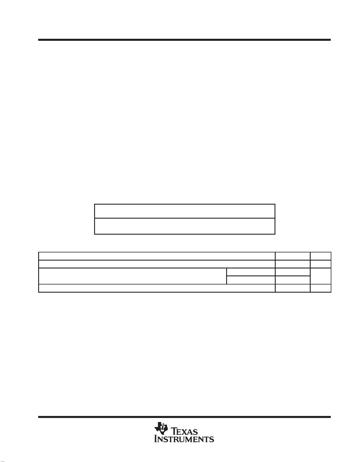
TLE2227, TLE2227Y, TLE2237, TLE2237Y
VIOt
CHIP FORM
‡
0°C to 70°C
EXCALIBUR LOW-NOISE HIGH-SPEED
PRECISION DUAL OPERATIONAL AMPLIFIERS
SLOS184 – FEBRUARY 1997
D
Outstanding Combination of DC Precision
and AC Performance:
Unity-Gain Bandwidth . . . 15 MHz Typ
V
. . . 3.3 nV/√Hz at f = 10 Hz Typ,
n
2.5 nV/√Hz
V
. . . 100 µV Typ
IO
A
. . . 45 V/µV Typ With RL = 2 kΩ
VD
38 V/µV Typ With R
D
Available in 16-Pin Small-Outline
at f = 1 kHz Typ
L
Wide-Body Package
D
Macromodels and Statistical Information
Included
D
Output Features Saturation Recovery
Circuitry
description
The TLE22x7C combines innovative circuit
design expertise and high-quality process control
techniques to produce a level of ac performance
and dc precision previously unavailable in dual
operational amplifiers. This device allows
upgrades to systems that use lower-precision
devices and is manufactured using Texas
Instruments state-of-the-art Excalibur process.
= 1 kΩ
P PACKAGE
(TOP VIEW)
1OUT
1IN–
1IN+
V
CC–
1OUT
1IN–
1IN+
V
NC – No internal connection
DW PACKAGE
(TOP VIEW)
NC
NC
CC–
NC
NC
1
2
3
4
1
2
3
4
5
6
7
8
16
15
14
13
12
11
10
8
7
6
5
9
V
2OUT
2IN–
2IN+
NC
NC
V
2OUT
2IN–
2IN+
NC
NC
CC+
CC+
In the area of dc precision, the TLE22x7C offers a typical offset voltage of 100 µV, a common-mode rejection
ratio of 115 dB (typ), a supply voltage rejection ratio of 120 dB (typ), and a dc gain of 45 V/µV (typ).
The ac performance is highlighted by a typical unity-gain bandwidth specification of 15 MHz, 55° of phase
margin, and noise voltage specifications of 3.3 nV/√Hz
and 2.5 nV/√Hz at frequencies of 10 Hz and 1 kHz,
respectively.
The TLE22x7C is available in a wide variety of packages, including the industry standard 16-pin small-outline
wide-body version for high-density system applications. This device is characterized for operation from 0°C to
70°C.
AVAILABLE OPTIONS
T
A
°
°
†
The DW package is available taped and reeled. Add R suffix to device type (e.g., TLE2227CDWR).
‡
Chip forms are tested at 25°C only.
yp
AT 25°C
100 µV TLE2227CDW TLE2227CP TLE2227Y
100 µV TLE2237CDW TLE2237CP TLE2237Y
SMALL OUTLINE
PACKAGED DEVICES
†
(DW)
PLASTIC DIP
(P)
(Y)
Please be aware that an important notice concerning availability, standard warranty, and use in critical applications of
Texas Instruments semiconductor products and disclaimers thereto appears at the end of this data sheet.
PRODUCTION DATA information is current as of publication date.
Products conform to specifications per the terms of Texas Instruments
standard warranty. Production processing does not necessarily include
testing of all parameters.
POST OFFICE BOX 655303 • DALLAS, TEXAS 75265
Copyright 1997, Texas Instruments Incorporated
1
TLE2227, TLE2227Y, TLE2237, TLE2237Y
EXCALIBUR LOW-NOISE HIGH-SPEED
PRECISION DUAL OPERATIONAL AMPLIFIERS
SLOS184 – FEBRUARY 1997
symbol (each amplifier)
IN+
IN–
+
OUT
–
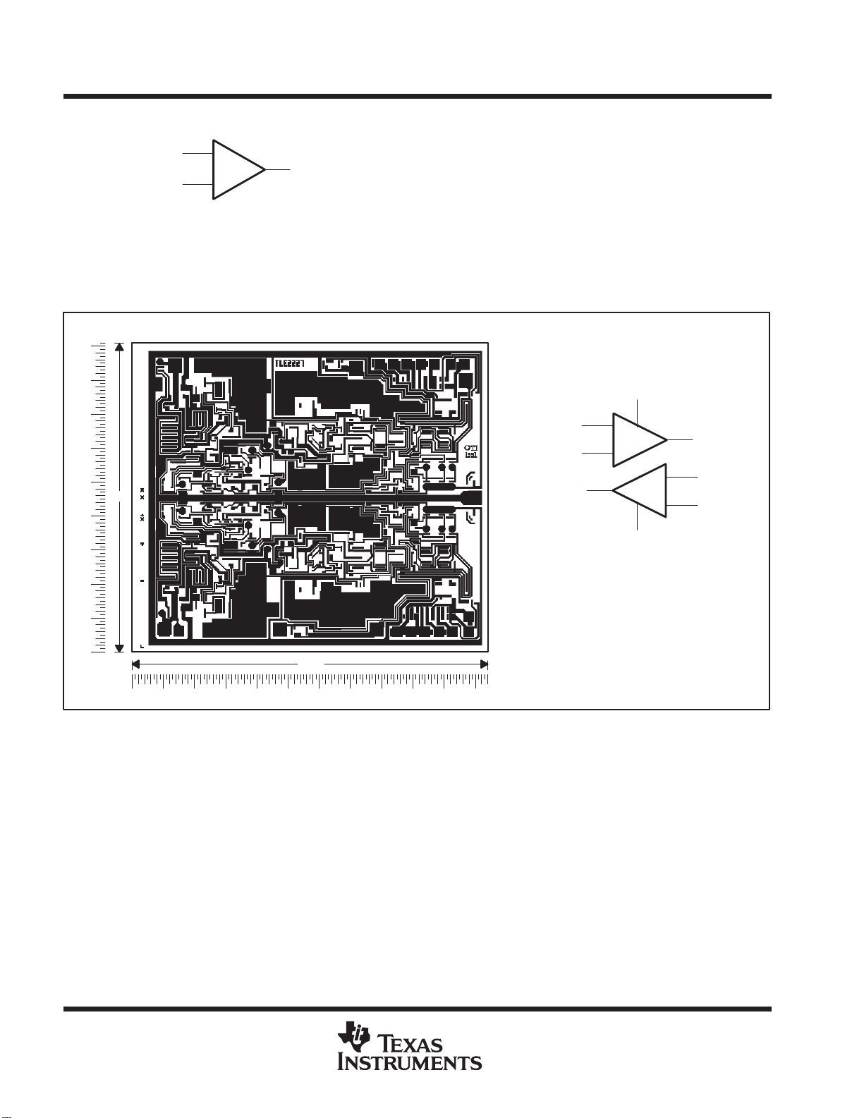
TLE2227Y chip information
This chip, properly assembled, displays characteristics similar to the TLE2227C. Thermal compression or
ultrasonic bonding may be used on the doped-aluminum bonding pads. Chips my be mounted with conductive
epoxy or a gold-silicon preform.
BONDING PAD ASSIGNMENTS
(7)
(8)
116
(6)
(5)
(4)
1IN+
1IN–
2OUT
(3)
(2)
(7)
V
CC+
(8)
+
–
V
CC–
(4)
(1)
(5)
+
(6)
–
1OUT
2IN+
2IN–
(1)
(2) (3)
104
CHIP THICKNESS: 15 TYPICAL
BONDING PADS: 4 × 4 MINIMUM
TJmax = 150°C
TOLERANCES ARE ±10%.
ALL DIMENSIONS ARE IN MILS.
2
POST OFFICE BOX 655303 • DALLAS, TEXAS 75265
TLE2227, TLE2227Y, TLE2237, TLE2237Y
EXCALIBUR LOW-NOISE HIGH-SPEED
PRECISION DUAL OPERATIONAL AMPLIFIERS
SLOS184 – FEBRUARY 1997
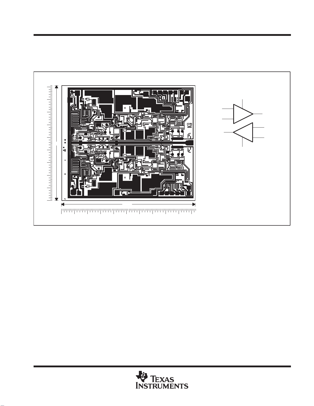
TLE2237Y chip information
ThIs chip, when properly assembled, displays characteristics similar to TLE2237. Thermal compression or
ultrasonic bonding may be used on the doped-aluminum bonding pads. The chip may be mounted with
conductive epoxy or a gold-silicon preform.
BONDING PAD ASSIGNMENTS
116
(8)
(1)
(7)
(6)
(2) (3)
104
(5)
(4)
V
CC+
1IN+
1IN–
2OUT
CHIP THICKNESS: 15 MILS TYPICAL
BONDING PADS: 4 × 4 MILS MINIMUM
TJmax = 150°C
TOLERANCES ARE ±10%.
ALL DIMENSIONS ARE IN MILS.
(3)
(2)
(7)
(8)
+
–
V
CC–
(4)
(1)
1OUT
(5)
+
–
(6)
2IN+
2IN–
POST OFFICE BOX 655303 • DALLAS, TEXAS 75265
3
T
l
R
l
D
7
11
94
4
POST OFFICE BOX 655303 DALLAS, TEXAS 75265
•
equivalent schematic (each amplifier)
Q14
Q12
R4
R5
Q13
Q17
Q18
Q15
Q16
R3
IN+
IN–
Q1
Q2
Q3
Q4
Q5
Q6
Q7
Q8
Q9
Q10
Q11
R1
R2
C1
Q20
Q21
Q22
R6
Q19
Q24Q23
Q26 Q29
R7
R9
Q27
R8 R11
Q28
Q25
C2
R10
Q30
R12
Q32
R13
Q31
Q33
C3
Q34
R15
R16
R17
C4
R18R14
Q36
Q35
V
Q37
CC+
Q38
R19
Q39
Q40
R20
Q41
Q42
Q43
R21
Q44
Q45
Q46
Q47
R22
Q48
R23
Q49
Q51
Q52
Q50
Q53
Q54
R25
Q58
Q55
Q56
Q59
Q57
Q60
R24 R26
Q61
Q62
OUT
TLE2227, TLE2227Y, TLE2237, TLE2237Y
EXCALIBUR LOW-NOISE HIGH-SPEED
PRECISION DUAL OPERATIONAL AMPLIFIERS
SLOS184 – FEBRUARY 1997
emp
ate
e
ease
ate:
–
–
V
CC–
ACTUAL DEVICE COMPONENT COUNT
COMPONENT TLE2227 TLE2237
Transistors 62 62
Resistors 24 24
Diodes 0 0
Capacitors 4 4
C
V
V
TLE2227, TLE2227Y, TLE2237, TLE2237Y
EXCALIBUR LOW-NOISE HIGH-SPEED
PRECISION DUAL OPERATIONAL AMPLIFIERS
SLOS184 – FEBRUARY 1997
absolute maximum ratings over operating free-air temperature range (unless otherwise noted)
Supply voltage, V
Supply voltage, V
Differential input voltage, V
Input voltage range, V
Input current, I
(each input) ±1 mA. . . . . . . . . . . . . . . . . . . . . . . . . . . . . . . . . . . . . . . . . . . . . . . . . . . . . . . . . . . . . . .
I
Output current, I
Total current into V
Total current out of V
Duration of short-circuit current at (or below) 25°C (see Note 3) unlimited. . . . . . . . . . . . . . . . . . . . . . . . . . . . . .
Continuous total dissipation See Dissipation Rating Table. . . . . . . . . . . . . . . . . . . . . . . . . . . . . . . . . . . . . . . . . . .
Operating free-air temperature range, T
Lead temperature 1,6 mm (1/16 inch) from case for 10 seconds 260°C. . . . . . . . . . . . . . . . . . . . . . . . . . . . . . .
†
Stresses beyond those listed under “absolute maximum ratings” may cause permanent damage to the device. These are stress ratings only, and
functional operation of the device at these or any other conditions beyond those indicated under “recommended operating conditions” is not
implied. Exposure to absolute-maximum-rated conditions for extended periods may affect device reliability.
NOTES: 1. All voltage values, except differential voltages, are with respect to the midpoint between V
2. Differential voltages are at IN+ with respect to IN–. Excessive current flows if a differential input voltage in excess of approximately
±1.2 V is applied between the inputs unless some limiting resistance is used.
3. The output can be shorted to either supply. Temperature and/or supply voltages must be limited to ensure that the maximum
dissipation rating is not exceeded.
(see Note 1) 19 V. . . . . . . . . . . . . . . . . . . . . . . . . . . . . . . . . . . . . . . . . . . . . . . . . . . . . . . . . . .
CC+
–19 V. . . . . . . . . . . . . . . . . . . . . . . . . . . . . . . . . . . . . . . . . . . . . . . . . . . . . . . . . . . . . . . . . . . . .
CC–
I
±50 mA. . . . . . . . . . . . . . . . . . . . . . . . . . . . . . . . . . . . . . . . . . . . . . . . . . . . . . . . . . . . . . . . . . . . . . .
O
CC+
CC–
PACKAGE
DW 1025 mW 8.2 mW/°C 656 mW
(see Note 2) ±1.2 V. . . . . . . . . . . . . . . . . . . . . . . . . . . . . . . . . . . . . . . . . . . . . . . . . .
ID
(any input) V
. . . . . . . . . . . . . . . . . . . . . . . . . . . . . . . . . . . . . . . . . . . . . . . . . . . . . . . . . . .
50 mA. . . . . . . . . . . . . . . . . . . . . . . . . . . . . . . . . . . . . . . . . . . . . . . . . . . . . . . . . . . . . . . . . . .
50 mA. . . . . . . . . . . . . . . . . . . . . . . . . . . . . . . . . . . . . . . . . . . . . . . . . . . . . . . . . . . . . . . . .
0°C to 70°C. . . . . . . . . . . . . . . . . . . . . . . . . . . . . . . . . . . . . . . . . . . . . .
A
CC+
DISSIPATION RATING TABLE
TA ≤ 25°C
POWER RATING
P 1000 mW 8.0 mW/°C 640 mW
DERATING FACTOR
ABOVE TA = 25°C
TA = 70°C
POWER RATING
and V
CC–
.
CC±
†
recommended operating conditions
Supply voltage, V
ommon-mode input voltage,
Operating free-air temperature, T
†
Full range is 0°C to 70°C.
CC±
IC
A
MIN MAX UNIT
±4 ±19 V
TA = 25°C ±11
TA = Full range
†
±10.5
0 70 °C
POST OFFICE BOX 655303 • DALLAS, TEXAS 75265
5
TLE2227, TLE2227Y, TLE2237, TLE2237Y
PARAMETER
TEST CONDITIONS
T
†
UNIT
VIOInput offset voltage
V
IIOInput offset current
nA
IIBInput bias current
nA
V
Common-mode input voltage range
R
Ω
V
R
kΩ
V
Maximum ositive eak out ut voltage
V
R
kΩ
R
1 kΩ
V
gg
V
R
kΩ
A
VD
gg g
V/µV
V
±10 V
R
kΩ
CMRR
Common-mode rejection ratio
V
V
min
R
Ω
dB
k
ygj
dB
ICCS
t
V
No load
A
EXCALIBUR LOW-NOISE HIGH-SPEED
PRECISION DUAL OPERATIONAL AMPLIFIERS
SLOS184 – FEBRUARY 1997
electrical characteristics at specified free-air temperature, V
p
α
c
z
†
NOTE 4: T ypical values are based on the input of fset voltage shift observed through 168 hours of operating life test at TA = 150°C extrapolated
Temperature coefficient of input offset
VIO
voltage
Input offset voltage long-term drift
(see Note 4)
p
p
ICR
Maximum positive peak output voltage
OM+
swing
Maximum negative peak output voltage
OM–
swing
Large-signal differential voltage
amplification
Input capacitance 25°C 8 pF
i
Open-loop output impedance IO = 0 25°C 50 Ω
o
Supply-voltage rejection
SVR
ratio (∆V
Full range is 0°C to 70°C.
CC±
upply curren
to TA = 25°C using the Arrhenius equation and assuming an activation energy of 0.96 eV.
p
/∆VIO)
VIC = 0, RS = 50 Ω
= 50
S
= 1
L
= 2
L
=
L
= 2
L
VO = ±11 V, RL = 2 kΩ 25°C 2.5 45
VO = ±10 V,
=
,
=
= ±4 V to ±18 V, RS = 50 Ω 25°C 94 120
= ±4 V to ±18 V,
= 0,
ICR
,
V
V
O
IC
CC±
CC±
O
RL = 2 kΩ Full range 2
= 1
L
= 50
S
RS = 50 Ω Full range 92
= ±15 V (unless otherwise noted)
±
CC
A
25°C 100 350
Full range 500
Full range 0.4 1 µV/°C
25°C
25°C 7.5 90
Full range 150
25°C 15 90
Full range 150
25°C
Full range
25°C 10.5
Full range 10
25°C 12
Full range 11
25°C –10.5 –13
Full range –10
25°C –12 –13.5
Full range –11
25°C 3.5 38
Full range 1
25°C 98 115
Full range 95
25°C 7.3 10.6
Full range 11.2
TLE2227C
MIN TYP MAX
0.006 1 µV/mo
–11
–13
to
to
11
13
–10.5
to
10.5
µ
m
6
POST OFFICE BOX 655303 • DALLAS, TEXAS 75265
PARAMETER
TEST CONDITIONS
T
†
UNIT
SR
Sl
R
C
100 pF
V/
VnEquivalent input noise voltage
25°C
V/√HZ
V
Peak-to-peak equivalent input noise voltage
f
25°C
50
250
nV
InEquivalent input noise current
25°C
A/√HZ
TLE2227, TLE2227Y, TLE2237, TLE2237Y
EXCALIBUR LOW-NOISE HIGH-SPEED
PRECISION DUAL OPERATIONAL AMPLIFIERS
SLOS184 – FEBRUARY 1997
operating characteristics at specified free-air temperature, V
ew rate
p
N(PP)
THD Total harmonic distortion
B
1
B
OM
φ
m
†
Full range is 0°C to 70°C.
NOTE 5: Measured distortion of the source used in the analysis is 0.002%.
Unity-gain bandwidth RL = 2 kΩ, CL = 100 pF 25°C 7 13 MHz
Maximum output-swing bandwidth RL = 2 kΩ 25°C 30 kHz
Phase margin RL = 2 kΩ CL = 100 pF 25°C 40°
p
p
p
= 2 kΩ,
L
RS = 20 Ω, f = 10 Hz
RS = 20 Ω, f = 1 kHz
= 0.1 Hz to 10 Hz
f = 10 Hz
f = 1 kHz
VO = ±10 V,
See Note 5
=
L
AVD = 1,
= ±15 V
±
CC
A
25°C 1.7 2.5
Full range 1.2
°
°
°
25°C <0.002%
MIN TYP MAX
TLE2227C
3.3 8
2.5 4.5
1.5 4
0.4 0.6
µs
n
p
POST OFFICE BOX 655303 • DALLAS, TEXAS 75265
7
TLE2227, TLE2227Y, TLE2237, TLE2237Y
PARAMETER
TEST CONDITIONS
T
†
UNIT
VIOInput offset voltage
V/°C
V
0
R
50 Ω
IIOInput offset current
nA
IIBInput bias current
nA
V
Common-mode input voltage range
R
Ω
V
R
kΩ
V
Maximum positive peak output voltage swing
V
R
kΩ
R
kΩ
V
Maximum negative peak output voltage swing
V
R
kΩ
AVDLarge-signal differential voltage amplification
V/µV
V
±10 V
R
1 kΩ
CMRR
Common-mode rejection ratio
IC ICR
,
dB
k
Suppl
oltage rejection ratio (∆V
/∆V
dB
ICCSupply current
V
No load
mA
EXCALIBUR LOW-NOISE HIGH-SPEED
PRECISION DUAL OPERATIONAL AMPLIFIERS
SLOS184 – FEBRUARY 1997
electrical characteristics at specified free-air temperature, V
p
α
C
z
†
NOTE 4. T ypical values are based on the input of fset voltage shift observed through 168 hours of operating life test at TA = 150°C extrapolated
Temperature coefficient of input offset voltage Full range 0.4 1
VIO
Input offset voltage long-term drift (see Note 4)
p
p
ICR
OM+
OM–
Input capacitance 25°C 8 pF
i
Open-loop output impedance IO = 0 25°C 50
O
pp
SVR
Full range is 0°C to 70°C.
y-v
pp
to TA = 25°C using the Arrhenius equation and assuming an activation energy of 0.96 eV.
p
p
p
p
p
p
p
CC±
IO
)
,
=
IC
= 50
S
= 1
L
= 2
L
= 1
L
= 2
L
VO = ±11V, RL = 2 kΩ 25°C 2.5 45
VO = ±10 V, RL = 2 kΩ Full range 2
=
O
V
= V
RS = 50 Ω
V
= ±4 V to ±18 V,
CC±
RS = 50 Ω
V
= ±4 V to ±18 V,
CC±
RS = 50 Ω
= 0,
O
,
min,
=
S
=
L
= ±15 V (unless otherwise noted)
±
CC
A
25°C 100 350 µV
Full range 500
25°C 0.006 1 µV/mo
25°C 7.5 90
Full range 150
25°C 15 90
Full range 150
25°C
Full range
25°C 10.5
Full range 10
25°C 12
Full range 11
25°C –10.5 –13
Full range –10
25°C –12 –13.5
Full range –11
25°C 3.5 38
Full range 1
25°C 98 115
Full range 95
25°C 94 120
Full range 92
25°C 7.3 10.6
Full range 11.2
TLE2237C
MIN TYP MAX
–11
–13
to
11
–10.5
10.5
to
13
to
°
µ
Ω
8
POST OFFICE BOX 655303 • DALLAS, TEXAS 75265
PARAMETER
TEST CONDITIONS
T
†
UNIT
SR
Slew rate
VD
,
,
V/µs
VnEquivalent input noise voltage
25°C
V/√H
InEquivalent input noise current
25°C
A/√H
THD
Total harmonic distortion
O
,
VD
,
25°C
002%
GBP
Gain-bandwidth product
,
L
,
25°C3550
MH
TLE2227, TLE2227Y, TLE2237, TLE2237Y
EXCALIBUR LOW-NOISE HIGH-SPEED
PRECISION DUAL OPERATIONAL AMPLIFIERS
SLOS184 – FEBRUARY 1997
operating characteristics at specified free-air temperature, V
A
= 5, RL = 2 kΩ,
CL = 100 pF
p
V
n(PP)
B
OM
φ
m
†
Full range is 0°C to 70°C.
NOTE 5. Measured distortion of the source used in the analysis was 0.002%.
Peak-to-peak equivalent input noise voltage f = 0.1 Hz to 10 Hz 25°C 50 250 nV
p
p
Maximum output-swing bandwidth RL = 2 kΩ 25°C 80 kHz
Phase margin RL = 2 kΩ, CL = 100 pF 25°C 40°
RS = 20 Ω, f = 10 Hz
RS = 20 Ω, f = 1 kHz
f = 10 Hz
f = 1 kHz
V
= ±10 V , A
See Note 5
f = 100 kHz, R
CL = 100 pF
= 5 V,
= 2 kΩ,
= ±15 V
±
CC
A
25°C 4 5
Full range 3
°
°
°
°
MIN TYP MAX
TLE2237C
3.3 8
2.5 4.5
1.5 4
0.4 0.6
<0.
n
z
p
z
z
POST OFFICE BOX 655303 • DALLAS, TEXAS 75265
9
TLE2227, TLE2227Y, TLE2237, TLE2237Y
PARAMETER
TEST CONDITIONS
UNIT
V
R
Ω
V
Maximum positive peak output voltage swing
V
V
Maximum negative peak output voltage swing
V
AVDLarge-signal differential voltage amplification
V/µV
PARAMETER
TEST CONDITIONS
UNIT
VnEquivalent input noise voltage
V/√HZ
V
Peak-to-peak equivalent input noise voltage
f
50
250
nV
InEquivalent input noise current
A/√HZ
EXCALIBUR LOW-NOISE HIGH-SPEED
PRECISION DUAL OPERATIONAL AMPLIFIERS
SLOS184 – FEBRUARY 1997
electrical characteristics, V
V
IO
I
IO
I
IB
V
ICR
OM+
OM–
ci
z
o
CMRR Common-mode rejection ratio VIC = V
k
SVR
I
CC
NOTE 4. T ypical values are based on the input of fset voltage shift observed through 168 hours of operating life test at TA = 150°C extrapolated
Input offset voltage 100 350 µV
Input offset voltage long-term drift (see Note 4)
Input offset current
Input bias current 15 90 nA
Common-mode input voltage range RS = 50 Ω
p
p
p
Input capacitance 8 pF
Open-loop output impedance IO = 0 50 Ω
Supply-voltage rejection ratio (∆V
Supply current VO = 0, No load 7.3 10.6 mA
to TA = 25°C using the Arrhenius equation and assuming an activation energy of 0.96 eV.
= ±15 V, TA = 25°C (unless otherwise noted)
CC±
= 0,
IC
p
p
p
/∆VIO) V
CC±
RL = 1 kΩ 10.5
RL = 2 kΩ 12
RL = 1 kΩ –10.5 –13
RL = 2 kΩ –12 –13.5
VO = ±11 V, RL = 2 kΩ 2.5 45
VO = ±10 V, RL = 1 kΩ 3.5 38
min, RS = 50 Ω 98 115 dB
ICR
= ±4 V to ±18 V, RS = 50 Ω 94 120 dB
CC±
= 50
S
TLE2227Y
MIN TYP MAX
0.006 1 µV/mo
7.5 90 nA
–11
–13
to
to
11
13
V
operating characteristics, V
SR Slew rate RL = 2 kΩ, CL = 100 pF 1.7 2.5 V/µs
p
N(PP)
THD Total harmonic distortion
B
1
B
OM
φ
m
NOTE 5 Measured distortion of the source used in the analysis is 0.002%.
Unity-gain bandwidth RL = 2 kΩ, CL = 100 pF 7 13 MHz
Maximum output-swing bandwidth RL = 2 kΩ 30 kHz
Phase margin RL = 2 kΩ CL = 100 pF 40°
p
p
p
= ±15 V, TA = 25°C
CC±
TLE2227Y
MIN TYP MAX
RS = 20 Ω, f = 10 Hz 3.3 8
RS = 20 Ω, f = 1 kHz 2.5 4.5
= 0.1 Hz to 10 Hz
f = 10 Hz 1.5 4
f = 1 kHz 0.4 0.6
VO = ±10 V,
See Note 5
AVD = 1,
<0.002%
n
p
10
POST OFFICE BOX 655303 • DALLAS, TEXAS 75265

PARAMETER
TEST CONDITIONS
UNIT
V
0
R
50 Ω
V
Maximum positive peak output voltage swing
V
V
Maximum negative peak output voltage swing
V
AVDLarge-signal differential voltage amplification
V/µV
PARAMETER
TEST CONDITIONS
UNIT
VnEquivalent input noise voltage
V/√H
InEquivalent input noise current
A/√H
TLE2227, TLE2227Y, TLE2237, TLE2237Y
EXCALIBUR LOW-NOISE HIGH-SPEED
PRECISION DUAL OPERATIONAL AMPLIFIERS
SLOS184 – FEBRUARY 1997
electrical characteristics at specified free-air temperature V
V
IO
I
IO
I
IB
V
ICR
OM+
OM–
C
i
z
O
CMRR Common-mode rejection ratio VIC = V
k
SVR
I
CC
NOTE 4. T ypical values are based on the input of fset voltage shift observed through 168 hours of operating life test at TA = 150°C extrapolated
Input offset voltage 100 350 µV
Input offset voltage long-term drift (see Note 4)
Input offset current
Input bias current 15 90 nA
Common-mode input voltage range RS = 50 Ω
p
p
Input capacitance 8 pF
Open-loop output impedance IO = 0 50 Ω
Supply-voltage rejection ratio (∆V
Supply current VO = 0, No load 7.3 10.6 mA
to TA = 25°C using the Arrhenius equation and assuming an activation energy of 0.96 eV.
p
p
p
p
/∆VIO) V
CC±
,
=
IC
RL = 1 kΩ 10.5
RL = 2 kΩ 12
RL = 1 kΩ –10.5 –13
RL = 2 kΩ –12 –13.5
VO = ±11 V, RL = 2 kΩ 2.5 45
VO = ±10 V, RL = 1 kΩ 3.5 38
min, RS = 50 Ω 98 115 dB
ICR
= ±4 V to ±18 V , RS = 50 Ω 94 120 dB
CC±
= ±15 V (unless otherwise noted)
CC±
TLE2237Y
MIN TYP MAX
=
S
0.006 1 µV/mo
7.5 90 nA
–11
–13
to
11
to
13
V
operating characteristics at specified free-air temperature V
SR Slew rate RL = 2 kΩ, CL = 100 pF 4 5 V/µs
p
V
n(PP)
THD Total harmonic distortion VO = ±10 V, AVD = 1, See Note 5 <0.002%
B
1
B
OM
φ
m
NOTE 5. Measured distortion of the source used in the analysis is 0.002%.
Peak-to-peak equivalent input noise voltage f = 0.1 Hz to 10 Hz 50 250 nV
p
Unity-gain bandwidth RL = 2 kΩ, CL = 100 pF 35 50 MHz
Maximum output-swing bandwidth RL = 2 kΩ 80 kHz
Phase margin RL = 2 kΩ, CL = 100 pF 40 °
RS = 20 Ω, f = 10 Hz 3.3 8
RS = 20 Ω, f = 1 kHz 2.5 4.5
f = 10 Hz 1.5 4
f = 1 kHz 0.4 0.6
CC±
= ±15 V
TLE2237Y
MIN TYP MAX
n
p
z
z
POST OFFICE BOX 655303 • DALLAS, TEXAS 75265
11

TLE2227, TLE2227Y, TLE2237, TLE2237Y
EXCALIBUR LOW-NOISE HIGH-SPEED
PRECISION DUAL OPERATIONAL AMPLIFIERS
SLOS184 – FEBRUARY 1997
PARAMETER MEASUREMENT INFORMATION
4 kΩ
15 V
–
V
+
I
–15 V
NOTE A: CL includes fixture capacitance.
CL = 100 pF
(see Note A)
Figure 1. Slew-Rate Test Circuit
10 kΩ
100 Ω
V
I
NOTE A: CL includes fixture capacitance.
–
+
15 V
–15 V
CL = 100 pF
(see Note A)
Figure 3. Unity-Gain Bandwidth and
Phase-Margin Test Circuit
V
4 kΩ
2 kΩ
15 V
–
V
O
+
–15 V
20 Ω20 Ω
O
Figure 2. Noise-Voltage Test Circuit
15 V
–
V
2 kΩ
O
V
+
I
–15 V
NOTE A: CL includes fixture capacitance.
CL = 100 pF
(see Note A)
V
O
2 kΩ
Figure 4. Small-Signal Pulse-
Response Test Circuit
12
POST OFFICE BOX 655303 • DALLAS, TEXAS 75265

TLE2227, TLE2227Y, TLE2237, TLE2237Y
EXCALIBUR LOW-NOISE HIGH-SPEED
PRECISION DUAL OPERATIONAL AMPLIFIERS
SLOS184 – FEBRUARY 1997
TYPICAL CHARACTERISTICS
Table of Graphs
FIGURE
V
IO
∆V
IO
I
IO
I
IB
I
I
V
O(PP)
V
OM
V
OM
A
VD
z
o
CMRR Common-mode rejection ratio vs Frequency 24
k
SVR
I
OS
I
CC
V
n
B
1
SR Slew rate vs Free-air temperature 44, 45
φ
m
Input offset voltage Distribution 5
Input offset voltage change vs Time after power on 6, 7
Input offset current vs Free-air temperature 8
Input bias current
Input current vs Differential input voltage 11
Maximum peak-to-peak output voltage vs Frequency 12
Maximum peak positive output voltage
Maximum peak negative output voltage
Large-signal differential voltage amplification
Output impedance vs Frequency 23
Supply-voltage rejection ratio vs Frequency 25
Short-circuit output current
Supply current
Voltage-follower small-signal pulse response vs Time 34, 35
Voltage-follower large-signal pulse response vs Time 36, 37
Equivalent input noise voltage vs Frequency 38
Noise voltage (referred to input) Over 10-second interval 39
Unity-gain bandwidth
Phase margin
Phase shift vs Frequency 18, 20, 21
vs Common-mode input voltage
vs Free-air temperature
vs Load resistance
vs Free-air temperature
vs Load resistance
vs Free-air temperature
vs Supply voltage
vs Load resistance
vs Frequency
vs Free-air temperature
vs Supply voltage
vs Elasped time
vs Free-air temperature
vs Supply voltage
vs Free-air temperature
vs Supply voltage
vs Load capacitance
vs Supply voltage
vs Load capacitance
9
10
13
15
14
16
17
19
18, 20, 21
22
26, 27
28, 29
30, 31
32
33
40, 41
42, 43
46
47, 48
POST OFFICE BOX 655303 • DALLAS, TEXAS 75265
13

TLE2227, TLE2227Y, TLE2237, TLE2237Y
EXCALIBUR LOW-NOISE HIGH-SPEED
PRECISION DUAL OPERATIONAL AMPLIFIERS
SLOS184 – FEBRUARY 1997
TYPICAL CHARACTERISTICS
16
1568 Amplifiers Tested From 2 Wafer Lots
V
CC±
14
TA = 25°C
DW Package
12
10
8
6
4
Percentage of Amplifiers – %
2
0
–120
INPUT OFFSET VOLTAGE CHANGE
6
Vµ
5
DISTRIBUTION OF
INPUT OFFSET VOLTAGE
= ±15 V
0 120906030–30–60–90
VIO – Input Offset Voltage – µV
Figure 5
vs
TIME AFTER POWER ON
12
Vµ
10
8
6
4
2
IO
∆V
XVIO – Change In Input Offset Voltage – uV
0
0
20
V
CC±
VIC = 0
16
INPUT OFFSET VOLTAGE CHANGE
vs
TIME AFTER POWER ON
V
= ± 15 V
CC±
TA = 25°C
DW Package
Sample Size = 50 Units
t – Time After Power On – s
Figure 6
INPUT OFFSET CURRENT
vs
FREE-AIR TEMPERATURE
= ±15 V
605040302010
IO
∆V
XVIO – Change In Input Offset Voltage – uV
14
4
3
2
V
= ±15 V
CC±
1
0
0
t – Time After Power On – s
TA = 25°C
P Package
Sample Size = 50 Units
From 2 Wafer Lots
18016014012010080604020
Figure 7
POST OFFICE BOX 655303 • DALLAS, TEXAS 75265
12
8
IO
4
IIO – Input Offset Current – nA
I
0
0
10 30 40 50 60 7020
TA – Free-Air Temperature – ° C
Figure 8

ООООО
ООООО
TLE2227, TLE2227Y, TLE2237, TLE2237Y
EXCALIBUR LOW-NOISE HIGH-SPEED
PRECISION DUAL OPERATIONAL AMPLIFIERS
SLOS184 – FEBRUARY 1997
TYPICAL CHARACTERISTICS
INPUT BIAS CURRENT
COMMON-MODE INPUT VOLTAGE
40
V
= ±15 V
CC±
TA = 25°C
35
30
25
20
15
10
IB
I
IIB – Input Bias Current – nA
5
0
–12
VIC – Common-Mode Input Voltage – V
Figure 9
INPUT CURRENT
DIFFERENTIAL INPUT VOLTAGE
1
V
= ±15 V
CC±
VIC = 0
0.8
TA = 25°C
0.6
vs
vs
INPUT BIAS CURRENT
vs
FREE-AIR TEMPERATURE
20
V
= ±15 V
CC±
VIC = 0
16
12
8
4
0
IB
I
IIB – Input Bias Current – nA
–4
–8
12840–4–8
010 304050607020
TA – Free-Air Temperature – ° C
Figure 10
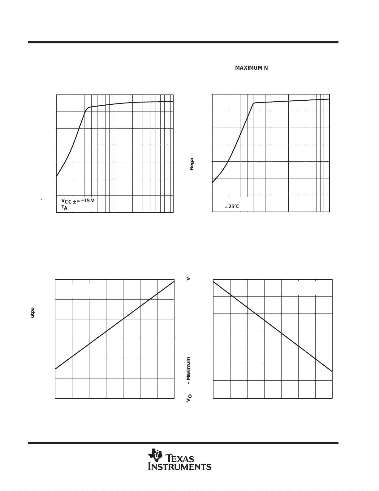
MAXIMUM PEAK-TO-PEAK
OUTPUT VOLTAGE
30
25
vs
FREQUENCY
V
= ±15 V
CC±
RL = 2 kΩ
TA = 25°C
0.4
0.2
0
–0.2
I
II – Input Current – mA
I
–0.4
–0.6
–0.8
–1
–1.8
VID – Differential Input Voltage – V
Figure 11
20
15
10
5
O(PP)
0
VO(PP) – Maximum Peak-to-Peak Output Voltage – V
1.81.20.60– 0.6–1.2
POST OFFICE BOX 655303 • DALLAS, TEXAS 75265
V
10 k
10 M1 M100 k
f – Frequency – Hz
Figure 12
15
TLE2227, TLE2227Y, TLE2237, TLE2237Y
EXCALIBUR LOW-NOISE HIGH-SPEED
PRECISION DUAL OPERATIONAL AMPLIFIERS
SLOS184 – FEBRUARY 1997
TYPICAL CHARACTERISTICS
14
12
10
8
6
4
2
OM +
VOM+ – Maximum Positive Peak Output Voltage – V
0
V
100
V
= ±15 V
CC±
TA = 25°C
MAXIMUM POSITIVE PEAK
OUTPUT VOLTAGE
vs
LOAD RESISTANCE
RL – Load Resistance – Ω
Figure 13
MAXIMUM NEGATIVE PEAK
OUTPUT VOLTAGE
vs
LOAD RESISTANCE
–14
–12
–10
–8
–6
–4
–2
V
= ±15 V
CC±
0
100
TA = 25°C
10 k1 k
RL – Load Resistance – Ω
OM –
VOM– – Maximum Negative Peak Output Voltage – V
10 k1 k
V
Figure 14
13.32
13.28
13.24
13.2
13.16
13.12
OM +
VOM+ – Maximum Positive Peak Output Voltage – V
13.08
V
MAXIMUM POSITIVE PEAK
OUTPUT VOLTAGE
vs
FREE-AIR TEMPERATURE
V
= ±15 V
CC±
RL = 2 kΩ
TA – Free-Air Temperature – ° C
Figure 15
706050403020100
–13.4
–13.45
–13.5
–13.55
–13.6
–13.65
–13.7
OM –
–13.75
VOM– – Maximum Negative Peak Output Voltage – V
V
MAXIMUM NEGATIVE PEAK
OUTPUT VOLTAGE
vs
FREE-AIR TEMPERATURE
V
CC±
RL = 2 kΩ
TA – Free-Air Temperature – ° C
Figure 16
= ±15 V
706050403020100
16
POST OFFICE BOX 655303 • DALLAS, TEXAS 75265
Á
Á
TLE2227, TLE2227Y, TLE2237, TLE2237Y
EXCALIBUR LOW-NOISE HIGH-SPEED
PRECISION DUAL OPERATIONAL AMPLIFIERS
SLOS184 – FEBRUARY 1997
TYPICAL CHARACTERISTICS
LARGE-SIGNAL DIFFERENTIAL
VOLTAGE AMPLIFICATION
vs
SUPPLY VOLTAGE
50
TA = 25°C
Vµ
40
V/
30
20
Voltage Amplification –
VD
A
AVD – Large-Signal differential
10
0
0
| V
| – Supply Voltage – V
CC±
Figure 17
LARGE-SIGNAL DIFFERENTIAL VOLTAGE
AMPLIFICATION AND PHASE SHIFT
FREQUENCY
160
RL = 2 kΩ
RL = 1 kΩ
20161284
vs
75°
120
A
VD
100
80
60
Voltage Amplification – dB
VD
40
A
AVD – Large-Signal Differential
20
0
0.1
V
= ±15 V
CC±
RL = 2 kΩ
CL = 100 pF
TA = 25°C
f – Frequency – Hz
Figure 18
Phase Shift
100°140
125°
150°
175°
Phase Shift
200°
225°
250°
100 k100
275°
100 M
POST OFFICE BOX 655303 • DALLAS, TEXAS 75265
17

TLE2227, TLE2227Y, TLE2237, TLE2237Y
EXCALIBUR LOW-NOISE HIGH-SPEED
PRECISION DUAL OPERATIONAL AMPLIFIERS
SLOS184 – FEBRUARY 1997
TYPICAL CHARACTERISTICS
LARGE-SIGNAL DIFFERENTIAL
VOLTAGE AMPLIFICATION
vs
LOAD RESISTANCE
50
V
= ±15 V
CC±
TA = 25°C
Vµ
40
V/
30
20
Voltage Amplification –
VD
A
AVD – Large-Signal differential
10
0
100
RL – Load Resistance – Ω
Figure 19
LARGE-SIGNAL DIFFERENTIAL VOLTAGE
AMPLIFICATION AND PHASE SHIFT
FREQUENCY
6
3
0
–3
–6
–9
Voltage Amplification – dB
VD
–12
A
AVD – Large-Signal Differential
–15
–18
10
Phase Shift
V
= ±15 V
CC±
RL = 2 kΩ
CL = 100 pF
TA = 25°C
f – Frequency – MHz
1 k 4 k400
TLE2227
vs
10 k
100°
125°
150°
100
175°
200°
225°
250°
275°
300°
Phase Shift
A
VD
704020
18
Figure 20
POST OFFICE BOX 655303 • DALLAS, TEXAS 75265
TLE2227, TLE2227Y, TLE2237, TLE2237Y
EXCALIBUR LOW-NOISE HIGH-SPEED
PRECISION DUAL OPERATIONAL AMPLIFIERS
SLOS184 – FEBRUARY 1997
TYPICAL CHARACTERISTICS
TLE2037
LARGE-SIGNAL DIFFERENTIAL VOLTAGE
AMPLIFICATION AND PHASE SHIFT
vs
FREQUENCY
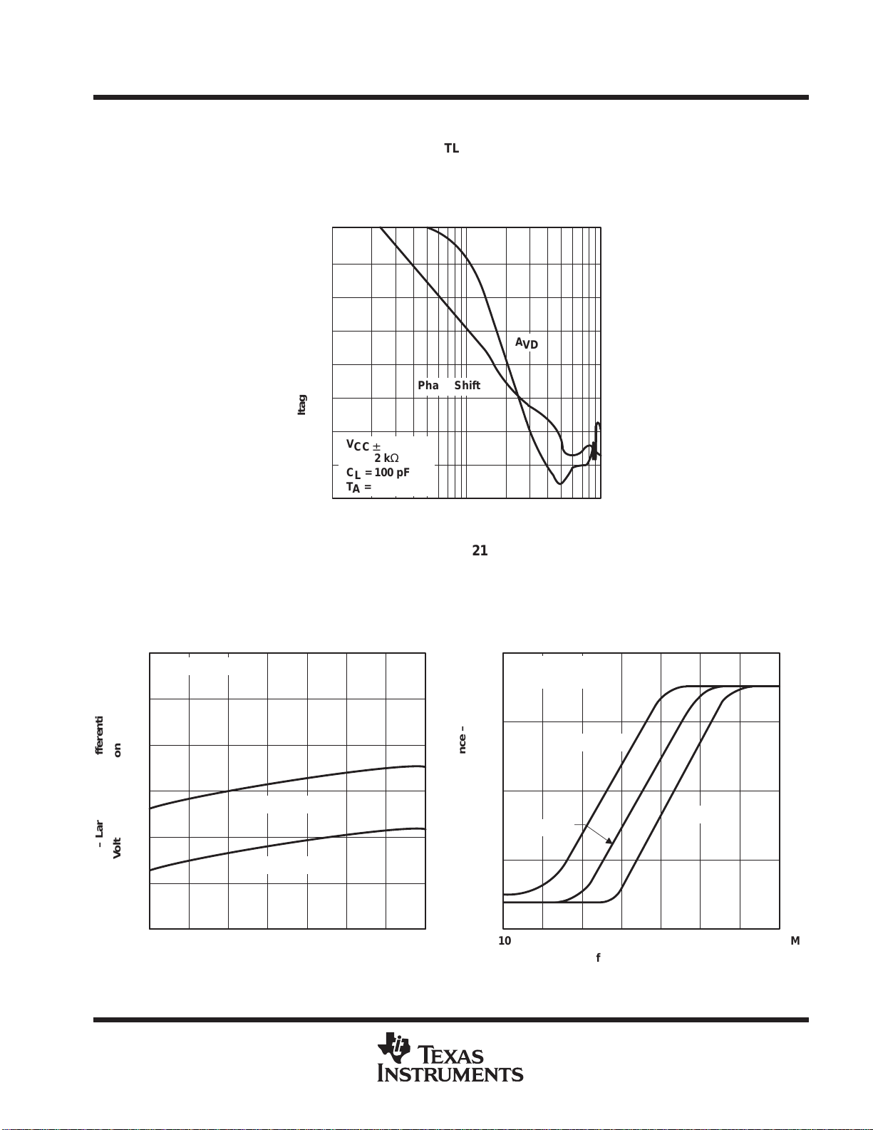
30
100°
100
125°
150°
175°
200°
225°
250°
275°
300°
Phase Shift
25
20
15
10
5
Voltage Amplification – dB
VD
0
A
AVD – Large-Signal Differential
– 10
– 5
V
CC±
RL = 2 kΩ
CL = 100 pF
TA = 25°C
1
Phase Shift
= ±15 V
f – Frequency – MHz
A
VD
40104
Figure 21
LARGE-SCALE DIFFERENTIAL
VOLTAGE AMPLIFICATION
vs
FREE-AIR TEMPERATURE
60
V
= ±15 V
CC±
55
Vµ
V/
50
100
V
CC±
TA = 25°C
Ω
10
OUTPUT IMPEDANCE
vs
FREQUENCY
= ±15 V
AVD = 100
45
40
Voltage Amplification –
VD
A
AVD – Large-Signal Differential
35
30
0
TA – Free-Air Temperature – ° C
Figure 22
RL = 2 kΩ
RL = 1 kΩ
1
AVD = 10
o
zo – Output Impedance – O
z
0.1
0.01
70605040302010
POST OFFICE BOX 655303 • DALLAS, TEXAS 75265
10
AVD = 1
f – Frequency – Hz
Figure 23
10 M1 M100 k10 k1 k100
100 M
19
TLE2227, TLE2227Y, TLE2237, TLE2237Y
EXCALIBUR LOW-NOISE HIGH-SPEED
PRECISION DUAL OPERATIONAL AMPLIFIERS
SLOS184 – FEBRUARY 1997
TYPICAL CHARACTERISTICS
COMMON-MODE REJECTION RATIO
vs
FREQUENCY
140
120
100
80
60
40
20
CMRR – Common-Mode Rejection Ratio – dB
0
10
f – Frequency – Hz
V
CC±
TA = 25°C
Figure 24
= ±15 V
10 M1 M100 k10 k1 k100
100 M
SUPPLY-VOLTAGE REJECTION RATIO
140
120
100
80
60
40
20
SVR
XXXX – Supply-Voltage Rejection Ratio – dB
k
0
10
f – Frequency – Hz
Figure 25
vs
FREQUENCY
k
SVR–
k
SVR+
V
= ±15 V
CC±
TA = 25°C
10 M1 M100 k10 k1 k100
100 M
SHORT-CIRCUIT OUTPUT CURRENT
vs
SUPPLY VOLTAGE
– 42
– 40
– 38
– 36
– 34
VID = 100 mV
– 32
– 30
VO = 0
TA = 25°C
P Package
0
|V
| – Supply Voltage – V
CC±
OS
IOS – Short-Circuit Output Current – mA
I
Figure 26
SHORT-CIRCUIT OUTPUT CURRENT
SUPPLY VOLTAGE
34
VID = –100 mV
VO = 0
33
TA = 25°C
P Package
32
31
30
29
28
27
26
OS
IOS – Short-Circuit Output Current – mA
I
25
24
2018161412108642
0
|V
CC±
vs
2018161412108642
| – Supply Voltage – V
Figure 27
20
POST OFFICE BOX 655303 • DALLAS, TEXAS 75265
TLE2227, TLE2227Y, TLE2237, TLE2237Y
EXCALIBUR LOW-NOISE HIGH-SPEED
PRECISION DUAL OPERATIONAL AMPLIFIERS
SLOS184 – FEBRUARY 1997
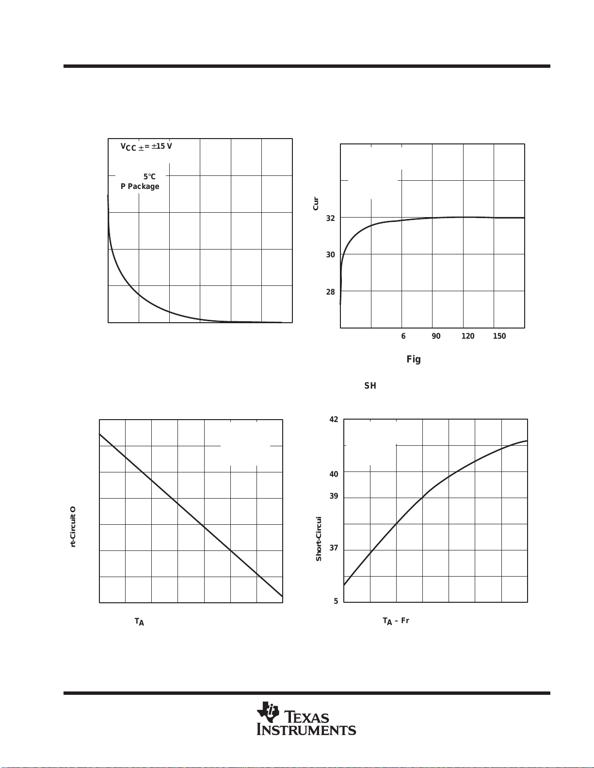
TYPICAL CHARACTERISTICS
SHORT-CIRCUIT OUTPUT CURRENT
vs
ELAPSED TIME
– 45
– 43
– 41
– 39
– 37
OS
IOS – Short-Circuit Output Current – mA
I
– 35
V
CC±
VID = 100 mV
VO = 0
TA = 25°C
P Package
0
= ±15 V
t – Time – s
Figure 28
SHORT-CIRCUIT OUTPUT CURRENT
vs
FREE-AIR TEMPERATURE
–55
–53
–51
150120906030
V
= ±15 V
CC±
VID = 100 mV
VO = 0
P Package
180
SHORT-CIRCUIT OUTPUT CURRENT
vs
ELAPSED TIME
36
V
= ±15 V
CC±
VID = –100 mV
VO = 0
34
TA = 25°C
P Package
32
30
28
OS
IOS – Short-Circuit Output Current – mA
I
26
0
t – Time – s
Figure 29
SHORT-CIRCUIT OUTPUT CURRENT
vs
FREE-AIR TEMPERATURE
42
V
= ±15 V
CC±
VID = –100 mV
41
VO = 0
P Package
40
150120906030
180
–49
–47
–45
–43
OS
IOS – Short-Circuit Output Current – mA
I
–41
0
TA – Free-Air Temperature – ° C
Figure 30
39
38
37
36
OS
IOS – Short-Circuit Output Current – mA
I
35
605040302010
70
POST OFFICE BOX 655303 • DALLAS, TEXAS 75265
TA – Free-Air Temperature – ° C
706050403020100
Figure 31
21
TLE2227, TLE2227Y, TLE2237, TLE2237Y
EXCALIBUR LOW-NOISE HIGH-SPEED
PRECISION DUAL OPERATIONAL AMPLIFIERS
SLOS184 – FEBRUARY 1997
TYPICAL CHARACTERISTICS
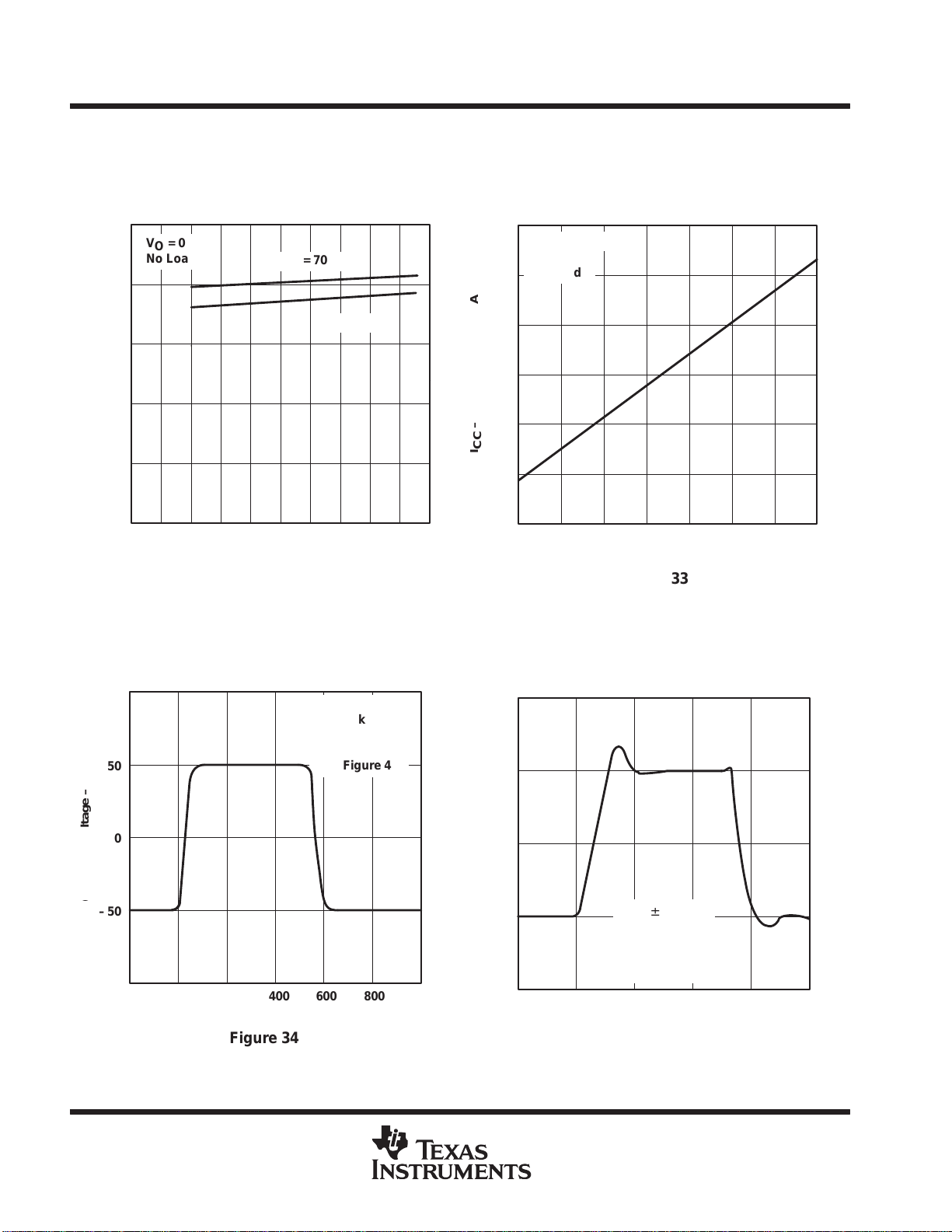
SUPPLY CURRENT
SUPPLY VOLTAGE
10
VO = 0
No Load
8
6
4
CC
ICC – Supply Current – mA
I
2
0
0
|V
| – Supply Voltage – V
CC±
Figure 32
vs
TA = 70°C
TA = 25°C
SUPPLY CURRENT
vs
FREE-AIR TEMPERATURE
8
V
= ±15 V
CC±
VO = 0
No Load
7.8
7.6
7.4
7.2
CC
ICC – Supply Current – mA
I
7
2018161412108642
6.8
706050403020100
TA – Free-Air Temperature – ° C
Figure 33
100
O
V) – Output Voltage – mV
–50
V
–100
50
TLE2227
VOLTAGE-FOLLOWER
SMALL-SIGNAL
PULSE RESPONSE
V
= ±15 V
CC±
RL = 2 kΩ
CL = 100 pF
TA = 25°C
See Figure 4
0
2000
t – Time – ns
800600400
1000
100
O
V) – Output Voltage – mV
–50
V
–100
50
0
Figure 34
TLE2237
VOLTAGE-FOLLOWER
SMALL-SIGNAL
PULSE RESPONSE
V
= ±15 V
CC±
AVD = 5
RL = 2 kΩ
CL = 100 pF
TA = 25°C
t – Time – ns
Figure 35
300100 4002000
22
POST OFFICE BOX 655303 • DALLAS, TEXAS 75265
TLE2227, TLE2227Y, TLE2237, TLE2237Y
EXCALIBUR LOW-NOISE HIGH-SPEED
PRECISION DUAL OPERATIONAL AMPLIFIERS
SLOS184 – FEBRUARY 1997
TYPICAL CHARACTERISTICS
15
10
5
0
–5
O
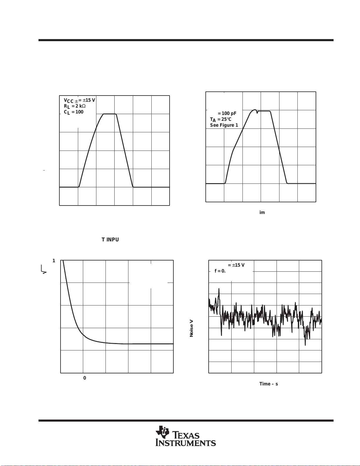
V) – Output Voltage – V
V
–10
–15
V
= ±15 V
CC±
RL = 2 kΩ
CL = 100 pF
TA = 25°C
See Figure 1
TLE2227
VOLTAGE-FOLLOWER
LARGE-SIGNAL
PULSE RESPONSE
t – Time – µs
Figure 36
TLE2237
VOLTAGE-FOLLOWER
LARGE-SIGNAL
PULSE RESPONSE
15
V
= ±15 V
CC±
AVD = 5
RL = 2 kΩ
10
CL = 100 pF
TA = 25°C
See Figure 1
5
0
–5
O
V) – Output Voltage – V
V
–10
–15
250 5 10 15 20
t – Time – µs
1002468
Figure 37
EQUIVALENT INPUT NOISE VOLTAGE
10
nV/ Hz
8
6
4
2
n
Vn – Equivalent Input Noise Voltage – nV/Hz
V
0
1
vs
FREQUENCY
V
RS = 20 Ω
TA = 25°C
See Figure 2
f – Frequency – Hz
Figure 38
CC±
= ±15 V
10 k1 k10010
100 k
50
40
30
20
10
0
– 10
Noise Voltage – nV
– 20
– 30
– 40
– 50
0
NOISE VOLTAGE
(REFERRED TO INPUT)
OVER A 10-SECOND INTERVAL
V
= ±15 V
CC±
f = 0.1 to 10 Hz
TA = 25°C
t – Time – s
Figure 39
8642
10
POST OFFICE BOX 655303 • DALLAS, TEXAS 75265
23

TLE2227, TLE2227Y, TLE2237, TLE2237Y
EXCALIBUR LOW-NOISE HIGH-SPEED
PRECISION DUAL OPERATIONAL AMPLIFIERS
SLOS184 – FEBRUARY 1997
TYPICAL CHARACTERISTICS
TLE2227
UNITY-GAIN BANDWIDTH
vs
UNITY-GAIN BANDWIDTH
SUPPLY VOLTAGE
20
RL = 2 kΩ
CL = 100 pF
TA = 25°C
18
See Figure 3
16
14
1
12
B1 – Unity-Gain Bandwidth – MHzB
10
0
| V
| – Supply Voltage – V
CC±
2018161412108642
52
f = 100 kHZ
RL = 2 kΩ
CL = 100 pF
TA = 25°C
51
50
49
1
B1 – Unity-Gain Bandwidth – MHzB
48
0
| V
Figure 40
TLE2237
vs
SUPPLY VOLTAGE
| – Supply Voltage – V
CC±
Figure 41
2018161412108642
TLE2227
UNITY-GAIN BANDWIDTH
UNITY-GAIN BANDWIDTH
vs
LOAD CAPACITANCE
B1 – Unity-Gain Bandwidth – MHzB
1
52
51
50
49
48
100
V
= ±15 V
CC±
RL = 2 kΩ
TA = 25°C
CL – Load Capacitance – pF
16
12
8
4
1
B1 – Unity-Gain Bandwidth – MHzB
0
100
CL – Load Capacitance – pF
1000
V
= ±15 V
CC±
RL = 2 kΩ
TA = 25°C
See Figure 3
10000
Figure 42
TLE2237
vs
LOAD CAPACITANCE
1000 10000
Figure 43
24
POST OFFICE BOX 655303 • DALLAS, TEXAS 75265

TLE2227, TLE2227Y, TLE2237, TLE2237Y
EXCALIBUR LOW-NOISE HIGH-SPEED
PRECISION DUAL OPERATIONAL AMPLIFIERS
SLOS184 – FEBRUARY 1997
TYPICAL CHARACTERISTICS
TLE2227
SLEW RATE
vs
FREE-AIR TEMPERATURE
3
V
= ±15 V
CC±
AVD = 5
RL = 2 kΩ
2.8
CL = 100 pF
See Figure 1
2.6
2.4
SR – Slew Rate – V/usµsV/
2.2
2
TA – Free-Air Temperature – ° C
706050403020100
8
V
AVD = 5
RL = 2 kΩ
7
CL = 100 pF
See Figure 1
6
5
SR – Slew Rate – V/usµsV/
4
3
FREE-AIR TEMPERATURE
= ±15 V
CC±
TA – Free-Air Temperature – ° C
Figure 44
TLE2237
SLEW RATE
vs
706050403020100
Figure 45
40°
RL = 2 kΩ
CL = 100 pF
38°
TA = 25°C
See Figure 3
36°
34°
32°
30°
m
φ
om – Phase Margin
28°
26°
24°
0
PHASE MARGIN
SUPPLY VOLTAGE
| V
| – Supply Voltage – V
CC±
Figure 46
vs
TLE2227
PHASE MARGIN
vs
LOAD CAPACITANCE
40°
35°
30°
25°
20°
m
om – Phase Margin
15°
φ
10°
5°
0°
2018161412108642
100
CL – Load Capacitance – pF
1000 10000
V
= ±15 V
CC±
RL = 2 kΩ
TA = 25°C
See Figure 3
Figure 47
POST OFFICE BOX 655303 • DALLAS, TEXAS 75265
25

TLE2227, TLE2227Y, TLE2237, TLE2237Y
EXCALIBUR LOW-NOISE HIGH-SPEED
PRECISION DUAL OPERATIONAL AMPLIFIERS
SLOS184 – FEBRUARY 1997
TYPICAL CHARACTERISTICS
TLE2237
PHASE MARGIN
LOAD CAPACITANCE
70°
V
= ±15 V
CC±
RL = 2 kΩ
60°
TA = 25°C
50°
40°
30°
m
om – Phase Margin
φ
20°
10°
vs
φ
m
0°
100
CL – Load Capacitance – pF
1000 10000
Figure 48
APPLICATION INFORMATION
TLE2227 macromodel information
Macromodel information provided was derived using Microsim
with Microsim
PSpice
. The Boyle macromodel (see Note 6) and subcircuit in Figure 49 and Figure 50 are
generated using the TLE2227C typical electrical and operating characteristics at 25°C. Using this information,
output simulations of the following key parameters can be generated to a tolerance of 20% (in most cases):
D
Maximum positive output voltage swing
D
Maximum negative output voltage swing
D
Slew rate
D
Quiescent power dissipation
D
Input bias current
D
Open-loop voltage amplification
Parts
, the model generation software used
D
Unity-gain bandwidth
D
Common-mode rejection ratio
D
Phase margin
D
DC output resistance
D
AC output resistance
D
Short-circuit output current limit
NOTE 6: G. R. Boyle, B. M. Cohn, D. O. Pederson, and J. E. Solomon,“Macromodeling of Integrated Circuit Operational Amplifiers”,
PSpice
Macromodels, simulation models, or other models provided by TI,
directly or indirectly, are not warranted by TI as fully representing all
of the specification and operating characteristics of the
semiconductor product to which the model relates.
26
of Solid-State Circuits
and
Parts
are trademarks of MicroSim Corporation.
, SC-9, 353 (1974).
POST OFFICE BOX 655303 • DALLAS, TEXAS 75265
IEEE Journal

APPLICATION INFORMATION
TLE2227 macromodel information (continued)
c1
4
3
rc2
12
vc
14
re2re1
10
ve
ceeree
dc
de
54
+–
V
V
CC+
IN+
IN–
CC–
rp
1
2
dp
rc1
11
Q1 Q2
13
lee
TLE2227, TLE2227Y, TLE2237, TLE2237Y
EXCALIBUR LOW-NOISE HIGH-SPEED
PRECISION DUAL OPERATIONAL AMPLIFIERS
SLOS184 – FEBRUARY 1997
99
vb
+
fb
–
C2
ga
7
vlim
ro2
8
5
hlim
OUT
+
–
ro1
90
+
–
egnd
9
+
+
r2
–
53
–
6
gcm
dip
91
+
–
dln
92
–
vip
+
vin
Figure 49. Boyle Macromodel
.subckt TLE2227 1 2 3 4 5
*
c1 11 12 4.003E-12
c2 6 7 20.00E-12
dc 5 53 dx
de 54 5 dx
dlp 90 91 dx
dln 92 90 dx
dp 4 3 dx
egnd 99 0 poly(2) (3,0) (4,0) 0 .5 .5
fb 7 99 poly(5) vb vc ve vlp vln 0 954.8E6 –1E9 1E9 1E9 –1E9
ga 6 0 11 12 2.062E-3
gcm 0 6 10 99 531.3E-12
iee 10 4 dc 56.01E-6
hlim 90 0 vlim 1K
q1 11 2 13 qx
q2 12 1 14 qx
r2 6 9 100.0E3
rc1 3 11 530.5
rc2 3 12 530.5
re1 13 10 –393.2
re2 14 10 –393.2
ree 10 99 3.571E6
ro1 8 5 25
ro2 7 99 25
rp 3 4 8.013E3
vb 9 0 dc 0
vc 3 53 dc 2.400
ve 54 4 dc 2.100
vlim 7 8 dc 0
vlp 91 0 dc 40
vln 0 92dc40
.model dx D(Is=800.0E-18)
.model qx NPN(Is=800.0E-18 Bf=7.000E3)
.ends
Figure 50. TLE2227 Macromodel Subcircuit
POST OFFICE BOX 655303 • DALLAS, TEXAS 75265
27

TLE2227, TLE2227Y, TLE2237, TLE2237Y
EXCALIBUR LOW-NOISE HIGH-SPEED
PRECISION DUAL OPERATIONAL AMPLIFIERS
SLOS184 – FEBRUARY 1997
TLE2037 macromodel information
Macromodel information provided is derived using
PSpice Parts
model generation software. The Boyle
macromodel (see Note 6) and subcircuit in Figure 51 and Figure 52 are generated using the TLE2237C typical
electrical and operating characteristics at 25°C. Using this information, output simulations of the following key
parameters can be generated to a tolerance of 20% (in most cases):
D
Maximum positive output voltage swing
D
Maximum negative output voltage swing
D
Slew rate
D
Quiescent power dissipation
D
Input bias current
D
Open-loop voltage amplification
NOTE 6. G. R. Boyle, B. M. Cohn, D. O. Pederson, and J. E. Solomon,“Macromodeling of Integrated Circuit Operational Amplifiers,”
V
V
of Solid-State Circuits
CC+
1
IN+
IN–
2
CC–
dp
, SC-9, 353 (1974).
3
rp
rc1
11
Q1 Q2
13
lee
c1
4
rc2
14
re2re1
12
10
ve
+
vc
ceeree
dc
de
54
+–
r2
–
53
D
Unity-gain bandwidth
D
Common-mode rejection ratio
D
Phase margin
D
DC output resistance
D
AC output resistance
D
Short-circuit output current limit
99
vb
+
fb
–
C2
ga
7
vlim
ro2
8
5
hlim
OUT
+
–
ro1
90
+
–
egnd
9
+
–
6
gcm
dlp
91
+
–
dln
vlp
IEEE Journal
92
–
vln
+
Macromodels, simulation models, or other models provided by TI,
directly or indirectly, are not warranted by TI as fully representing all
of the specification and operating characteristics of the
semiconductor product to which the model relates.
28
Figure 51. Boyle Macromodel
POST OFFICE BOX 655303 • DALLAS, TEXAS 75265

TLE2227, TLE2227Y, TLE2237, TLE2237Y
EXCALIBUR LOW-NOISE HIGH-SPEED
PRECISION DUAL OPERATIONAL AMPLIFIERS
SLOS184 – FEBRUARY 1997
APPLICATION INFORMATION
TLE2037 macromodel information (continued)
.subckt TLE2227 1 2 3 4 5
*
c1 11 12 4.003E-12
c2 6 7 20.00E-12
dc 5 53 dx
de 54 5 dx
dlp 90 91 dx
dln 92 90 dx
dp 4 3 dx
egnd 99 0 poly(2) (3,0) (4,0) 0 .5 .5
fb 7 99 poly(5) vb vc ve vlp vln 0 954.8E6 –1E9 1E9 1E9 –1E9
ga 6 0 11 12 2.062E-3
gcm 0 6 10 99 531.3E-12
iee 10 4 dc 56.01E-6
hlim 90 0 vlim 1K
q1 11 2 13 qx
q2 12 1 14 qx
r2 6 9 100.0E3
rc1 3 11 530.5
rc2 3 12 530.5
re1 13 10 –393.2
re2 14 10 –393.2
ree 10 99 3.571E6
ro1 8 5 25
ro2 7 99 25
rp 3 4 8.013E3
vb 9 0 dc 0
vc 3 53 dc 2.400
ve 54 4 dc 2.100
vlim 7 8 dc 0
vlp 91 0 dc 40
vln 0 92dc40
.model dx D(Is=800.0E-18)
.model qx NPN(Is=800.0E-18 Bf=7.000E3)
.ends
Figure 52. TLE2237 Macromodel Subcircuit
POST OFFICE BOX 655303 • DALLAS, TEXAS 75265
29

TLE2227, TLE2227Y, TLE2237, TLE2237Y
EXCALIBUR LOW-NOISE HIGH-SPEED
PRECISION DUAL OPERATIONAL AMPLIFIERS
SLOS184 – FEBRUARY 1997
APPLICATION INFORMATION
voltage-follower applications
The TLE22x7C circuitry includes input-protection diodes to limit the voltage across the input transistors;
however, no provision is made in the circuit to limit the current if these diodes are forward biased. This condition
can occur when the device is operated in the voltage-follower configuration and driven with a fast, large-signal
pulse. A feedback resistor is recommended to limit the current to a maximum of 1 mA to prevent degradation
of the device. Also, this feedback resistor forms a pole with the input capacitance of the device. For feedback
resistor values greater than 10 kΩ, this pole degrades the amplifier’s phase margin. This problem can be
alleviated by adding a capacitor (20 pF to 50 pF) in parallel with the feedback resistor (see Figure 53).
CF = 20 to 50 pF
IF ≤ 1 mA
R
F
V
CC+
–
V
O
V
I
+
V
CC–
Figure 53. Voltage-Follower Circuit
30
POST OFFICE BOX 655303 • DALLAS, TEXAS 75265

IMPORTANT NOTICE
T exas Instruments and its subsidiaries (TI) reserve the right to make changes to their products or to discontinue
any product or service without notice, and advise customers to obtain the latest version of relevant information
to verify, before placing orders, that information being relied on is current and complete. All products are sold
subject to the terms and conditions of sale supplied at the time of order acknowledgement, including those
pertaining to warranty, patent infringement, and limitation of liability.
TI warrants performance of its semiconductor products to the specifications applicable at the time of sale in
accordance with TI’s standard warranty. T esting and other quality control techniques are utilized to the extent
TI deems necessary to support this warranty . Specific testing of all parameters of each device is not necessarily
performed, except those mandated by government requirements.
CERT AIN APPLICATIONS USING SEMICONDUCTOR PRODUCTS MAY INVOLVE POTENTIAL RISKS OF
DEATH, PERSONAL INJURY, OR SEVERE PROPERTY OR ENVIRONMENTAL DAMAGE (“CRITICAL
APPLICATIONS”). TI SEMICONDUCTOR PRODUCTS ARE NOT DESIGNED, AUTHORIZED, OR
WARRANTED TO BE SUITABLE FOR USE IN LIFE-SUPPORT DEVICES OR SYSTEMS OR OTHER
CRITICAL APPLICA TIONS. INCLUSION OF TI PRODUCTS IN SUCH APPLICATIONS IS UNDERST OOD TO
BE FULLY AT THE CUSTOMER’S RISK.
In order to minimize risks associated with the customer’s applications, adequate design and operating
safeguards must be provided by the customer to minimize inherent or procedural hazards.
TI assumes no liability for applications assistance or customer product design. TI does not warrant or represent
that any license, either express or implied, is granted under any patent right, copyright, mask work right, or other
intellectual property right of TI covering or relating to any combination, machine, or process in which such
semiconductor products or services might be or are used. TI’s publication of information regarding any third
party’s products or services does not constitute TI’s approval, warranty or endorsement thereof.
Copyright 1998, Texas Instruments Incorporated
 Loading...