

TLE2027, TLE2037, TLE2027A, TLE2037A, TLE2027Y, TLE2037Y
CHIP
0°C to 70°C
40°C to 105°C
55 C to 125 C
EXCALIBUR LOW-NOISE HIGH-SPEED
PRECISION OPERATIONAL AMPLIFIERS
SLOS192A – FEBRUARY 1997 REVISED MARCH 2002
D
Outstanding Combination of dc Precision
and AC Performance:
Unity-Gain Bandwidth . . . 15 MHz Typ
V
n
3.3 nV/√Hz at f = 10 Hz Typ,. . . .
2.5 nV/√Hz at f = 1 kHz Typ
V
IO
A
VD
25 µV Max. . . .
45 V/µV Typ With RL = 2 kΩ,. . .
OFFSET N1
IN –
IN +
V
CC –
19 V/µV Typ With RL = 600 Ω
D
Available in Standard-Pinout Small-Outline
Package
D
Output Features Saturation Recovery
Circuitry
D
Macromodels and Statistical information
description
The TLE20x7 and TLE20x7A contain innovative
circuit design expertise and high-quality process
control techniques to produce a level of ac
performance and dc precision previously unavailable in single operational amplifiers. Manufactured using Texas Instruments state-of-the-art
Excalibur process, these devices allow upgrades
to systems that use lower-precision devices.
In the area of dc precision, the TLE20x7 and
TLE20x7A offer maximum offset voltages of
100 µV and 25 µV, respectively, common-mode
rejection ratio of 131 dB (typ), supply voltage
rejection ratio of 144 dB (typ), and dc gain of
45 V/µV (typ).
AVAILABLE OPTIONS
PACKAGED DEVICES
T
A
–
–
†
The D packages are available taped and reeled. Add R suffix to device type (e.g., TLE2027ACDR).
‡
Chip forms are tested at 25°C only.
VIOmax AT
25
°C
25 µV
100 µV
25 µV
100 µV
25 µV
100 µV
SMALL
OUTLINE
TLE2027ACD
TLE2037ACD
TLE2027CD
TLE2037CD
TLE2027AID
TLE2037AID
TLE2027ID
TLE2037ID
TLE2027AMD
TLE2037AMD
TLE2027MD
TLE2037MD
†
(D)
CHIP
CARRIER
(FK)
—
—
—
—
—
—
—
—
TLE2027AMFK
TLE2037AMFK
TLE2027MFK
TLE2037MFK
NC
IN–
NC
IN+
NC
CERAMIC
DIP
(JG)
—
—
—
—
—
—
—
—
TLE2027AMJG
TLE2037AMJG
TLE2027MJG
TLE2037MJG
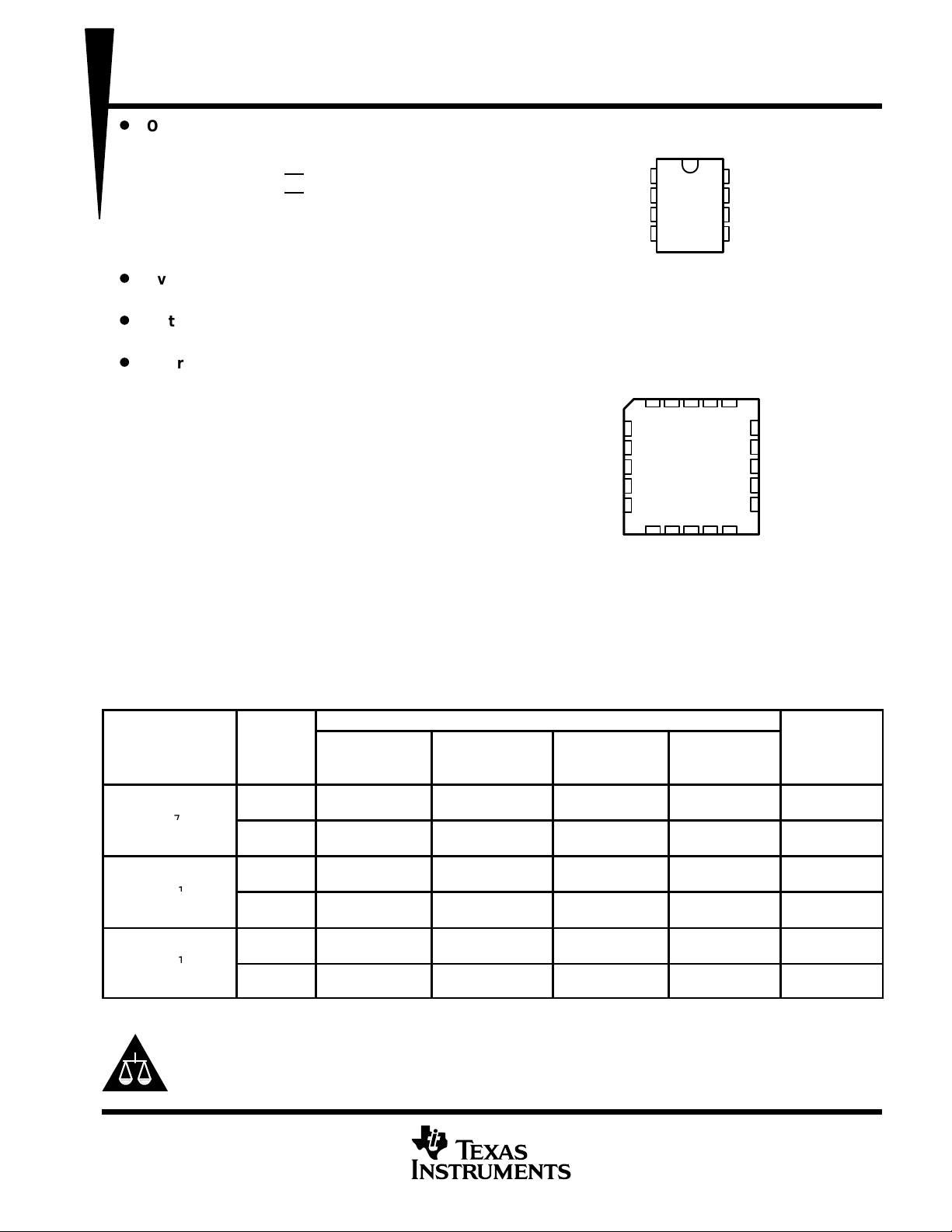
D, JG, OR P PACKAGE
(TOP VIEW)
1
2
3
4
FK PACKAGE
(TOP VIEW)
NC
OFFSET N1
3 2 1 20 19
4
5
6
7
8
910111213
NC
CC –
V
TLE2027ACP
TLE2037ACP
TLE2027CP
TLE2037CP
TLE2027AIP
TLE2037AIP
TLE2027IP
TLE2037IP
TLE2027AMP
TLE2037AMP
TLE2027MP
TLE2037MP
OFFSET N2
8
V
7
OUT
6
NC
5
NCNCNC
OFFSET N2
18
17
16
15
14
NC
NC
PLASTIC
DIP
(P)
CC +
NC
V
CC+
NC
OUT
NC
‡
FORM
(Y)
TLE2027Y
TLE2037Y
TLE2027Y
TLE2037Y
—
—
—
—
Please be aware that an important notice concerning availability, standard warranty, and use in critical applications of
Texas Instruments semiconductor products and disclaimers thereto appears at the end of this data sheet.
PRODUCTION DATA information is current as of publication date.
Products conform to specifications per the terms of Texas Instruments
standard warranty. Production processing does not necessarily include
testing of all parameters.
POST OFFICE BOX 655303 • DALLAS, TEXAS 75265
Copyright 2002, Texas Instruments Incorporated
1
TLE2027, TLE2037, TLE2027A, TLE2037A, TLE2027Y, TLE2037Y
EXCALIBUR LOW-NOISE HIGH-SPEED
PRECISION OPERATIONAL AMPLIFIERS
SLOS192A – FEBRUARY 1997 REVISED MARCH 2002
description (continued)
The ac performance of the TLE2027 and TLE2037 is highlighted by a typical unity-gain bandwidth specification
of 15 MHz, 55° of phase margin, and noise voltage specifications of 3.3 nV/√Hz
of 10 Hz and 1 kHz respectively . The TLE2037 and TLE2037A have been decompensated for faster slew rate
(–7.5 V/µs, typical) and wider bandwidth (50 MHz). To ensure stability, the TLE2037 and TLE2037A should be
operated with a closed-loop gain of 5 or greater.
Both the TLE20x7 and TLE20x7A are available in a wide variety of packages, including the industry-standard
8-pin small-outline version for high-density system applications. The C-suffix devices are characterized for
operation from 0°C to 70°C. The I-suffix devices are characterized for operation from –40°C to 105°C. The
M-suffix devices are characterized for operation over the full military temperature range of –55°C to 125°C.
symbol
OFFSET N1
and 2.5 nV/√Hz at frequencies
IN +
IN –
OFFSET N2
+
OUT
–
2
POST OFFICE BOX 655303 • DALLAS, TEXAS 75265
TLE2027, TLE2037, TLE2027A, TLE2037A, TLE2027Y, TLE2037Y
EXCALIBUR LOW-NOISE HIGH-SPEED
PRECISION OPERATIONAL AMPLIFIERS
SLOS192A – FEBRUARY 1997 REVISED MARCH 2002
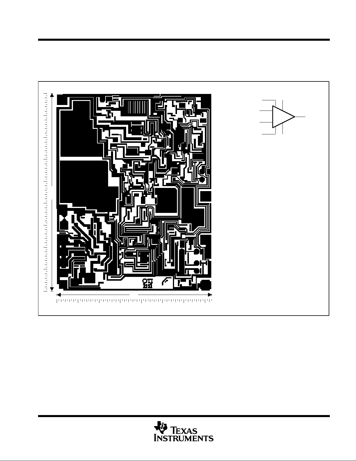
TLE202xY chip information
This chip, when properly assembled, displays characteristics similar to the TLE202xC. Thermal compression
or ultrasonic bonding may be used on the doped-aluminum bonding pads. The chip may be mounted with
conductive epoxy or a gold-silicon preform.
BONDING PAD ASSIGNMENTS
(1)
V
(6)
(4)
(7)(8)
(6)
OFFSET N1
IN+
IN–
OFFSET N2
(3)
(2)
(8)
(5)
CC+
(7)
+
–
(4)
V
CC–
(6)
OUT
90
(7)
(1) (2) (3)
(8)
73
(4)
(3)
(2)
(1)
CHIP THICKNESS: 15 MILS TYPICAL
BONDING PADS: 4 × 4 MILS MINIMUM
TJmax = 150°C
TOLERANCES ARE ±10%.
ALL DIMENSIONS ARE IN MILS.
PIN (4) IS INTERNALLY CONNECTED
TO BACKSIDE OF CHIP.
POST OFFICE BOX 655303 • DALLAS, TEXAS 75265
3
T
l
R
l
D
7
11
94
4
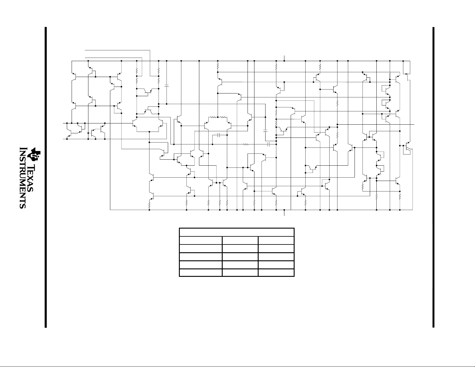
equivalent schematic
SLOS192A – FEBRUARY 1997 REVISED MARCH 2002
TLE2027, TLE2037, TLE2027A, TLE2037A, TLE2027Y, TLE2037Y
EXCALIBUR LOW-NOISE HIGH-SPEED
PRECISION OPERATIONAL AMPLIFIERS
emp
POST OFFICE BOX 655303 DALLAS, TEXAS 75265
•
OFFSET N2
OFFSET N1
IN +
Q1
IN –
Q2
Q3
Q4
Q5
Q6
Q7
Q8
Q9
Q10
Q11
R1
R2
Q14
Q12
Q15
Q16
R3
R4
R5
Q13
Q17
Q18
C1
Q20
Q21
Q22
R6
Q19
R9
Q27
R8 R11
Q25 Q28
C2
Q24Q23
Q26 Q29
Q30
Q32
R13
Q31
C3
Q34
Q33
R15
Q36
R16
R17
C4
R18R14R12R10R7
V
Q35
V
CC+
Q38
Q37
CC
ate
R20
Q50
Q53
Q54
R25
Q52
R24 R26
Q55
Q56
Q57
Q58
Q59
Q60
Q61
OUT
Q62
Q42
Q46
R21
Q39
Q44
Q43
Q47
Q41
Q40
R19
–
Q45
Q49
R22
Q48
Q51
R23
e
ease
ate:
–
–
ACTUAL DEVICE COMPONENT COUNT
COMPONENT TLE2027 TLE2037
Transistors 61 61
Resistors 26 26
epiFET 1 1
Capacitors 4 4
TLE2027, TLE2037, TLE2027A, TLE2037A, TLE2027Y, TLE2037Y
UNIT
Common-mode input voltage, V
V
EXCALIBUR LOW-NOISE HIGH-SPEED
PRECISION OPERATIONAL AMPLIFIERS
SLOS192A – FEBRUARY 1997 REVISED MARCH 2002
absolute maximum ratings over operating free-air temperature range (unless otherwise noted)
Supply voltage, V
Supply voltage, V
Differential input voltage, V
Input voltage range, V
Input current, I
I
Output current, I
Total current into V
Total current out of V
Duration of short-circuit current at (or below) 25°C (see Note 3) unlimited. . . . . . . . . . . . . . . . . . . . . . . . . . . .
Continuous total power dissipation See Dissipation Rating Table. . . . . . . . . . . . . . . . . . . . . . . . . . . . . . . . . . . . .
Operating free-air temperature range, T
Storage temperature range, T
Case temperature for 60 seconds, T
Lead temperature 1,6 mm (1/16 inch) from case for 10 seconds: D or P package 260°C. . . . . . . . . . . . . . . .
Lead temperature 1,6 mm (1/16 inch) from case for 60 seconds: JG package 300°C. . . . . . . . . . . . . . . . . . .
†
Stresses beyond those listed under “absolute maximum ratings” may cause permanent damage to the device. These are stress ratings only, and
functional operation of the device at these or any other conditions beyond those indicated under “recommended operating conditions” is not
implied. Exposure to absolute-maximum-rated conditions for extended periods may affect device reliability.
NOTES: 1. All voltage values, except differential voltages, are with respect to the midpoint between V
2. Differential voltages are at IN+ with respect to IN–. Excessive current flows if a differential input voltage in excess of approximately
±1.2 V is applied between the inputs unless some limiting resistance is used.
3. The output may be shorted to either supply. Temperature and/or supply voltages must be limited to ensure that the maximum
dissipation rating is not exceeded.
(see Note 1) 19 V. . . . . . . . . . . . . . . . . . . . . . . . . . . . . . . . . . . . . . . . . . . . . . . . . . . . . . . . .
CC+
– 19 V. . . . . . . . . . . . . . . . . . . . . . . . . . . . . . . . . . . . . . . . . . . . . . . . . . . . . . . . . . . . . . . . . . . .
CC–
I
(see Note 2) ±1.2 V. . . . . . . . . . . . . . . . . . . . . . . . . . . . . . . . . . . . . . . . . . . . . . . . . .
ID
(any input) V
. . . . . . . . . . . . . . . . . . . . . . . . . . . . . . . . . . . . . . . . . . . . . . . . . . . . . . . . .
(each Input) ±1 mA. . . . . . . . . . . . . . . . . . . . . . . . . . . . . . . . . . . . . . . . . . . . . . . . . . . . . . . . . . . . . .
± 50 mA. . . . . . . . . . . . . . . . . . . . . . . . . . . . . . . . . . . . . . . . . . . . . . . . . . . . . . . . . . . . . . . . . . . . .
O
50 mA. . . . . . . . . . . . . . . . . . . . . . . . . . . . . . . . . . . . . . . . . . . . . . . . . . . . . . . . . . . . . . . . . . .
CC+
50 mA. . . . . . . . . . . . . . . . . . . . . . . . . . . . . . . . . . . . . . . . . . . . . . . . . . . . . . . . . . . . . . . . .
CC–
: C suffix 0°C to 70°C. . . . . . . . . . . . . . . . . . . . . . . . . . . . . . . . . . . . . .
A
I suffix – 40°C to 105°C . . . . . . . . . . . . . . . . . . . . . . . . . . . . . . . . . .
M suffix – 55°C to 125°C. . . . . . . . . . . . . . . . . . . . . . . . . . . . . . . . . .
– 65°C to 150°C. . . . . . . . . . . . . . . . . . . . . . . . . . . . . . . . . . . . . . . . . . . . . . . . . .
stg
: FK package 260°C. . . . . . . . . . . . . . . . . . . . . . . . . . . . . . . . . . . . . . . . . .
C
CC +
and V
CC –
.
CC±
†
DISSIPATION RATING TABLE
PACKAGE
D 725 mW 5.8 mW/°C 464 mW 261 mW 145 mW
FK 1375 mW 11.0 mW/°C 880 mW 495 mW 275 mW
JG 1050 mW 8.4 mW/°C 672 mW 378 mW 210 mW
P 1000 mW 8.0 mW/°C 640 mW 360 mW 200 mW
TA ≤ 25°C
POWER RATING
DERATING FACTOR
ABOVE TA = 25°C
TA = 70°C
POWER RATING
TA = 105°C
POWER RATING
POWER RATING
recommended operating conditions
C SUFFIX I SUFFIX M SUFFIX
MIN MAX MIN MAX MIN MAX
Supply voltage, V
Operating free-air temperature, T
‡
Full range is 0°C to 70°C for C-suffix devices, –40°C to 105°C for I-suffix devices, and –55°C to 125°C for M-suffix devices.
CC±
p
IC
A
TA = 25°C –11 11 –11 11 –11 11
TA = Full range
‡
±4 ± 19 ±4 ±19 ±4 ±19 V
–10.5 10.5 –10.4 10.4 –10.2 10.2
0 70 –40 105 –55 125 °C
TA = 125°C
POST OFFICE BOX 655303 • DALLAS, TEXAS 75265
5
TLE2027, TLE2037, TLE2027A, TLE2037A, TLE2027Y, TLE2037Y
PARAMETER
TEST CONDITIONS
T
†
UNIT
VIOInput offset voltage
V
IIOInput offset current
nA
IIBInput bias current
nA
V
R
50 Ω
V
R
600 Ω
V
V
R
2 kΩ
R
600 Ω
V
g
V
R
2 kΩ
A
gg
V
±10 V, R
1 kΩ
V/µV
O
,
CMRR
j
IC ICR
,
dB
k
ygj
dB
ICCSupply current
V
0
No load
mA
EXCALIBUR LOW-NOISE HIGH-SPEED
PRECISION OPERATIONAL AMPLIFIERS
SLOS192A – FEBRUARY 1997 REVISED MARCH 2002
TLE20x7C electrical characteristics at specified free-air temperature, V
= ±15 V (unless
±
CC
otherwise noted)
A
p
α
C
z
o
SVR
†
Full range is 0°C to 70°C.
NOTE 4: Typical values are based on the input offset voltage shift observed through 168 hours of operating life test at TA = 150°C extrapolated
Temperature coefficient of
VIO
input offset voltage
Input offset voltage
long-term drift (see Note 4)
p
p
Common-mode input
ICR
voltage range
Maximum positive peak
OM +
output voltage swing
Maximum negative peak
OM –
output voltage swing
Large-signal differential
VD
voltage amplification
Input capacitance 25°C 8 8 pF
i
Open-loop output
impedance
Common-mode rejection V
ratio
Supply-voltage rejection
ratio (∆V
pp
to TA = 25°C using the Arrhenius equation and assuming an activation energy of 0.96 eV .
CC
/∆V
IO
±
VIC = 0, RS = 50 Ω
=
S
=
L
=
L
=
L
=
L
VO = ±11 V, RL = 2 kΩ 25°C 5 45 10 45
VO = ±10 V, RL = 2 kΩ Full range 2 4
=
O
V
= ±10 V,
RL = 600 Ω
IO = 0 25°C 50 50
= V
RS = 50 Ω
V
= ±4 V to ±18 V,
CC±
RS = 50 Ω
V
)
= ±4 V to ±18 V,
CC±
RS = 50 Ω
,
=
O
min,
=
L
25°C 20 100 10 25
Full range 145 70
Full range 0.4 1 0.2 1 µV/°C
25°C 0.006 1 0.006 1 µV/mo
25°C 6 90 6 90
Full range 150 150
25°C 15 90 15 90
Full range 150 150
25°C
Full range
25°C 10.5 12.9 10.5 12.9
Full range 10 10
25°C 12
Full range 11 11
25°C –10.5 –13 –10.5 –13
Full range –10 –10
25°C – 12 –13.5 – 12 –13.5
Full range – 11 – 11
25°C 3.5 38 8 38
Full range 1 2.5
25°C 2 19 5 19
Full range 0.5 2
25°C 100 131 117 131
Full range 98 114
25°C 94 144 110 144
Full range 92 106
25°C 3.8 5.3 3.8 5.3
Full range 5.6 5.6
TLE20x7C TLE20x7AC
MIN TYP MAX MIN TYP MAX
–11
11
–10.5
10.5
–13
to
to
13
to
13.2
–11
to
11
–10.5
to
10.5
12 13.2
–13
to
13
µ
Ω
6
POST OFFICE BOX 655303 • DALLAS, TEXAS 75265
TLE2027, TLE2037, TLE2027A, TLE2037A, TLE2027Y, TLE2037Y
PARAMETER
TEST CONDITIONS
UNIT
C
100 pF
L
,
V
q
V/√H
I
q
A/√H
THD
Total harmonic distortion
B
yg
L
,
MHz
g
B
g
R
2 kΩ
kHz
φ
gyg
L
EXCALIBUR LOW-NOISE HIGH-SPEED
PRECISION OPERATIONAL AMPLIFIERS
SLOS192A – FEBRUARY 1997 REVISED MARCH 2002
TLE20x7C operating characteristics at specified free-air temperature, V
(unless otherwise specified)
TLE20x7C TLE20x7AC
MIN TYP MAX MIN TYP MAX
RL = 2 kΩ,
See Figure 1
SR Slew rate at unity gain
n
V
N(PP)
n
1
OM
m
NOTE 5: Measured distortion of the source used in the analysis was 0.002%.
Equivalent input noise voltage (see Figure 2)
Peak-to-peak equivalent input noise voltage
Equivalent input noise current
Unity-gain bandwidth R
(see Figure 3)
Maximum output-swin
bandwidth
Phase margin at unity gain RL = 2 kΩ,
(see Figure 3)
RL = 2 kΩ,
C
TA = 0°C to 70°C,
See Figure 1
RS = 20 Ω, f = 10 Hz 3.3 8 3.3 4.5
RS = 20 Ω, f = 1 kHz
f = 0.1 Hz to 10 Hz 50 250 50 130 nV
f = 10 Hz 10 25 10 25
f = 1 kHz
VO = +10 V,
AVD = 1,
See Note 5
VO = +10 V,
AVD = 5,
See Note 5
CL = 100 pF
CL = 100 pF
=
L
= 100 pF,
= 2 kΩ,
=
L
p
,
TLE2027 1.7 2.8 1.7 2.8
TLE2037 6 7.5 6 7.5
TLE2027 1.2 1.2
TLE2037 5 5
2.5 4.5 2.5 3.8
0.8 1.8 0.8 1.8
TLE2027 <0.002% <0.002%
TLE2037 <0.002% <0.002%
TLE2027 7 13 9 13
TLE2037 35 50 35 50
TLE2027 30 30
TLE2037 80 80
TLE2027 55° 55°
TLE2037 50° 50°
= ±15 V, TA = 25°C
CC ±
n
p
V/µs
z
z
POST OFFICE BOX 655303 • DALLAS, TEXAS 75265
7
TLE2027, TLE2037, TLE2027A, TLE2037A, TLE2027Y, TLE2037Y
PARAMETER
TEST CONDITIONS
T
†
UNIT
VIOInput offset voltage
V
IIOInput offset current
nA
IIBInput bias current
nA
V
R
50 Ω
V
R
600 Ω
V
V
R
2 kΩ
R
600 Ω
V
g
V
R
2 kΩ
A
gg
V
±10 V, R
1 kΩ
V/µV
V
±10 V, R
600 Ω
CMRR
j
IC ICR
,
dB
k
ygj
dB
ICCSupply current
V
0
No load
mA
EXCALIBUR LOW-NOISE HIGH-SPEED
PRECISION OPERATIONAL AMPLIFIERS
SLOS192A – FEBRUARY 1997 REVISED MARCH 2002
TLE20x7I electrical characteristics at specified free-air temperature, V
= ±15 V (unless
CC±
otherwise noted)
A
p
α
C
z
o
SVR
†
Full range is – 40°C to 105°C.
NOTE 4: Typical values are based on the input offset voltage shift observed through 168 hours of operating life test at TA = 150°C extrapolated
Temperature coefficient of
VIO
input offset voltage
Input offset voltage
long-term drift (see Note 4)
p
p
Common-mode input
ICR
voltage range
Maximum positive peak
OM +
output voltage swing
Maximum negative peak
OM –
output voltage swing
Large-signal differential
VD
voltage amplification
Input capacitance 25°C 8 8 pF
i
Open-loop output
impedance
Common-mode rejection V
ratio
Supply-voltage rejection
ratio (∆V
pp
to TA = 25°C using the Arrhenius equation and assuming an activation energy of 0.96 eV .
CC
/∆VIO)
±
VIC = 0, RS = 50 Ω
=
S
=
L
=
L
=
L
=
L
VO = ±11 V, RL = 2 kΩ 25°C 5 45 10 45
VO = ±10 V, RL = 2 kΩ Full range 2 3.5
=
O
=
O
IO = 0 25°C 50 50
= V
RS = 50 Ω
V
= ±4 V to ±18 V,
CC±
RS = 50 Ω
V
= ±4 V to ±18 V,
CC±
RS = 50 Ω
,
=
O
min,
=
L
=
L
25°C 20 100 10 25
Full range 180 105
Full range 0.4 1 0.2 1 µV/°C
25°C 0.006 1 0.006 1 µV/mo
25°C 6 90 6 90
Full range 150 150
25°C 15 90 15 90
Full range 150 150
25°C
Full range
25°C 10.5 12.9 10.5 12.9
Full range 10 10
25°C 12
Full range 11 11
25°C –10.5 –13 –10.5 –13
Full range –10 –10
25°C – 12 –13.5 – 12 –13.5
Full range – 11 – 11
25°C 3.5 38 8 38
Full range 1 2.2
25°C 2 19 5 19
Full range 0.5 1.1
25°C 100 131 117 131
Full range 96 113
25°C 94 144 110 144
Full range 90 105
25°C 3.8 5.3 3.8 5.3
Full range 5.6 5.6
TLE20x7I TLE20x7AI
MIN TYP MAX MIN TYP MAX
–11
–10.4
10.4
–13
to
11
to
to
13
13.2
–11
to
11
–10.4
to
10.4
12 13.2
–13
to
13
µ
Ω
8
POST OFFICE BOX 655303 • DALLAS, TEXAS 75265
TLE2027, TLE2037, TLE2027A, TLE2037A, TLE2027Y, TLE2037Y
PARAMETER
TEST CONDITIONS
UNIT
C
100 pF
L
,
V
q
V/√H
I
q
A/√H
THD
Total harmonic distortion
B
yg
L
,
MHz
g
B
g
R
2 kΩ
kHz
y
φ
gy
L
,
EXCALIBUR LOW-NOISE HIGH-SPEED
PRECISION OPERATIONAL AMPLIFIERS
SLOS192A – FEBRUARY 1997 REVISED MARCH 2002
TLE20x7I operating characteristics at specified free-air temperature, V
(unless otherwise specified)
TLE20x7I TLE20x7AI
MIN TYP MAX MIN TYP MAX
RL = 2 kΩ,
See Figure 1
SR Slew rate at unity gain
n
V
N(PP)
n
1
OM
m
NOTE 5: Measured distortion of the source used in the analysis was 0.002%.
Equivalent input noise
voltage (see Figure 2)
Peak-to-peak equivalent
input noise voltage
Equivalent input noise
current
Unity-gain bandwidth R
(see Figure 3)
Maximum output-swin
bandwidth
Phase margin at unit
gain (see Figure 3)
RL = 2 kΩ,
C
TA = –40°C to 85°C,
See Figure 1
RS = 20 Ω, f = 10 Hz 3.3 8 3.3 4.5
RS = 20 Ω, f = 1 kHz
f = 0.1 Hz to 10 Hz 50 250 50 130 nV
f = 10 Hz 10 25 10 25
f = 1 kHz
VO = +10 V,
AVD = 1,
See Note 5
VO = +10 V,
AVD = 5,
See Note 5
CL = 100 pF
R
CL = 100 pF
=
L
= 100 pF,
= 2 kΩ,
=
L
= 2 kΩ,
p
,
TLE2027 1.7 2.8 1.7 2.8
TLE2037 6 7.5 6 7.5
TLE2027 1.1 1.1
TLE2037 4.7 4.7
2.5 4.5 2.5 3.8
0.8 1,8 0.8 1.8
TLE2027 < 0.002% < 0.002%
TLE2037 < 0.002% < 0.002%
TLE2027 7 13 9 13
TLE2037 35 50 35 50
TLE2027 30 30
TLE2037 80 80
TLE2027 55° 55°
TLE2037 50° 50°
= ±15 V, TA = 25°C
CC ±
n
p
V/µs
z
z
POST OFFICE BOX 655303 • DALLAS, TEXAS 75265
9
TLE2027, TLE2037, TLE2027A, TLE2037A, TLE2027Y, TLE2037Y
PARAMETER
TEST CONDITIONS
T
†
UNIT
VIOInput offset voltage
V
IIOInput offset current
nA
IIBInput bias current
nA
V
R
50 Ω
V
R
600 Ω
V
V
R
2 kΩ
R
600 Ω
V
g
V
R
2 kΩ
VD
voltage am lification
V
±10 V, R
1 kΩ
µ
V
±10 V, R
600 Ω
25°C219519
CMRR
j
IC ICR
,
dB
k
ygj
dB
ICCSupply current
V
0
load
mA
EXCALIBUR LOW-NOISE HIGH-SPEED
PRECISION OPERATIONAL AMPLIFIERS
SLOS192A – FEBRUARY 1997 REVISED MARCH 2002
TLE20x7M electrical characteristics at specified free-air temperature, V
= ±15 V (unless
±
CC
otherwise noted)
A
p
α
A
Ci
z
o
SVR
* On products compliant to MIL-PRF-38535, this parameter is not production tested.
†
Full range is – 55°C to 125°C.
NOTE 4: Typical values are based on the input offset voltage shift observed through 168 hours of operating life test at TA = 150°C extrapolated
Temperature coefficient of
VIO
input offset voltage
Input offset voltage
long-term drift (see Note 4)
p
p
Common-mode input
ICR
voltage range
Maximum positive peak
OM +
output voltage swing
Maximum negative peak
OM –
output voltage swing
Large-signal differential
VD
Input capacitance 25°C 8 8 pF
Open-loop output
impedance
Common-mode rejection V
ratio
Supply-voltage rejection
ratio (∆V
to TA = 25°C using the Arrhenius equation and assuming an activation energy of 0.96 eV .
pp
CC
p
/∆V
IO
±
VIC = 0, RS = 50 Ω
=
S
=
L
=
L
=
L
=
L
VO = ±11 V, RL = 2 kΩ 25°C 5 45 10 45
VO = ±10 V, RL = 2 kΩ Full range 2.5 3.5
=
O
=
O
IO = 0 25°C 50 50
= V
RS = 50 Ω
V
= ±4 V to ±18 V,
CC±
RS = 50 Ω
V
)
= ±4 V to ±18 V,
CC±
RS = 50 Ω
, No
=
O
min,
=
L
=
L
25°C 20 100 10 25
Full range 200 105
Full range 0.4 1* 0.2 1* µV/°C
25°C 0.006 1* 0.006 1* µV/mo
25°C 6 90 6 90
Full range 150 150
25°C 15 90 15 90
Full range 150 150
25°C
Full range
25°C 10.5 12.9 10.5 12.9
Full range 10 10
25°C 12 13.2 12 13.2
Full range 11 11
25°C –10.5 –13 –10.5 –13
Full range –10 –10
25°C – 12 –13.5 – 12 –13.5
Full range – 11 – 11
25°C 3.5 38 8 38
Full range 1.8 2.2
25°C 100 131 117 131
Full range 96 113
25°C 94 144 110 144
Full range 90 105
25°C 3.8 5.3 3.8 5.3
Full range 5.6 5.6
TLE20x7M TLE20x7AM
MIN TYP MAX MIN TYP MAX
–11
–10.3
10.3
–13
to
11
to
to
13
–11
11
–10.4
10.4
–13
to
to
to
13
µ
V/µV
Ω
10
POST OFFICE BOX 655303 • DALLAS, TEXAS 75265

TLE2027, TLE2037, TLE2027A, TLE2037A, TLE2027Y, TLE2037Y
PARAMETER
TEST CONDITIONS
UNIT
C
100 pF
L
,
V
q
V/√H
I
q
A/√H
THD
Total harmonic distortion
B
yg
L
,
MHz
g
B
g
R
2 kΩ
kHz
φ
gy
L
EXCALIBUR LOW-NOISE HIGH-SPEED
PRECISION OPERATIONAL AMPLIFIERS
SLOS192A – FEBRUARY 1997 REVISED MARCH 2002
TLE20x7M operating characteristics at specified free-air temperature, V
(unless otherwise specified)
TLE20x7M TLE20x7AM
MIN TYP MAX MIN TYP MAX
RL = 2 kΩ,
See Figure 1
SR Slew rate at unity gain
n
V
N(PP)
n
1
OM
m
* On products compliant to MIL-PRF-38535, this parameter is not production tested.
NOTE 5: Measured distortion of the source used in the analysis was 0.002%.
Equivalent input noise
voltage (see Figure 2)
Peak-to-peak equivalent
input noise voltage
Equivalent input noise
current
Unity-gain bandwidth R
(see Figure 3)
Maximum output-swin
bandwidth
Phase margin at unity RL = 2 kΩ,
gain (see Figure 3)
RL = 2 kΩ,
C
TA = –55°C to 125°C,
See Figure 1
RS = 20 Ω, f = 10 Hz 3.3 8* 3.3 4.5*
RS = 20 Ω, f = 1 kHz
f = 0.1 Hz to 10 Hz 50 250* 50 130* nV
f = 10 Hz 1.5 4* 1.5 4*
f = 1 kHz
VO = +10 V,
AVD = 1,
See Note 5
VO = +10 V,
AVD = 5,
See Note 5
CL = 100 pF
CL = 100 pF
=
L
= 100 pF,
= 2 kΩ,
=
L
p
,
TLE2027 1.7 2.8 1.7 2.8
TLE2037 6* 7.5 6* 7.5
TLE2027 1 1
TLE2037 4.4* 4.4*
2.5 4.5* 2.5 3.8*
0.4 0.6* 0.4 0.6*
TLE2027 < 0.002% < 0.002%
TLE2037 < 0.002% < 0.002%
TLE2027 7* 13 9* 13
TLE2037 35 50 35 50
TLE2027 30 30
TLE2037 80 80
TLE2027 55° 55°
TLE2037 50° 50°
= ±15 V, TA = 25°C
CC ±
n
p
V/µs
z
z
POST OFFICE BOX 655303 • DALLAS, TEXAS 75265
11

TLE2027, TLE2037, TLE2027A, TLE2037A, TLE2027Y, TLE2037Y
PARAMETER
TEST CONDITIONS
UNIT
IC
,
S
V
Maximum positive peak output voltage swing
V
V
Maximum negative peak output voltage swing
V
AVDLarge-signal differential voltage am lification
V/µV
EXCALIBUR LOW-NOISE HIGH-SPEED
PRECISION OPERATIONAL AMPLIFIERS
SLOS192A – FEBRUARY 1997 REVISED MARCH 2002
TLE20x7Y electrical characteristics, V
V
I
IO
I
IB
V
C
z
o
CMRR Common-mode rejection ratio
k
SVR
I
CC
NOTE 4: Typical values are based on the input offset voltage shift observed through 168 hours of operating life test at TA = 150°C extrapolated
Input offset voltage 20 µV
IO
Input offset voltage
long-term drift (see Note 4)
Input offset current
Input bias current 15 nA
Common-mode input voltage range RS = 50 Ω
ICR
p
OM +
OM –
Input capacitance 8 pF
i
Open-loop output impedance IO = 0 50
Supply-voltage rejection ratio (∆V
Supply current VO = 0, No load 3.8 mA
to TA = 25°C using the Arrhenius equation and assuming an activation energy of 0.96 eV .
p
p
p
p
p
/∆V
CC
±
= ±15 V, TA = 25°C (unless otherwise noted)
±
CC
MIN TYP MAX
V
IO
= 0, R
R
= 600 Ω 12.9
L
RL = 2 kΩ
RL = 600 Ω –13
RL = 2 kΩ –13.5
VO = ±11 V, RL = 2 kΩ 45
VO = ±10 V, RL = 1 kΩ 38
VO = ±10 V,
RL = 600 Ω
VIC = V
ICR
RS = 50 Ω
V
= ±4 V to ±18 V,
)
CC±
RS = 50 Ω
= 50 Ω
min,
TLE20x7Y
0.006 µV/mo
6 nA
–13
to
13
13.2
19
131 dB
144 dB
V
Ω
12
POST OFFICE BOX 655303 • DALLAS, TEXAS 75265
TLE2027, TLE2037, TLE2027A, TLE2037A, TLE2027Y, TLE2037Y
PARAMETER
TEST CONDITIONS
UNIT
SR
Slew rate at unity gain
L
,
L
,
V/µs
VnEquivalent input noise voltage (see Figure 2)
V/√H
InEquivalent input noise current
A/√H
THD
Total harmonic distortion
B1Unity-gain bandwidth (see Figure 3)
R
2 kΩ,C
100 pF
MHz
BOMMaximum output-swing bandwidth
R
2 kΩ
kHz
φ
Phase margin at unity gain (see Figure 3)
R
L
C
L
100 F
EXCALIBUR LOW-NOISE HIGH-SPEED
PRECISION OPERATIONAL AMPLIFIERS
SLOS192A – FEBRUARY 1997 REVISED MARCH 2002
TLE20x7Y operating characteristics at specified free-air temperature, V
R
= 2 kΩ,C
See Figure 1
p
V
N(PP)
m
NOTE 5: Measured distortion of the source used in the analysis was 0.002%.
Peak-to-peak equivalent input noise voltage f = 0.1 Hz to 10 Hz 50 nV
p
p
RS = 20 Ω, f = 10 Hz 3.3
RS = 20 Ω, f = 1 kHz 2.5
f = 10 Hz 10
f = 1 kHz 0.8
VO = +10 V, AVD = 1,
See Note 5
VO = +10 V, AVD = 5,
See Note 5
=
L
=
L
= 2 kΩ,
= 100 pF,
=
L
=
TLE2027 2.8
TLE2037 7.5
TLE2027 <0.002%
TLE2037 <0.002%
TLE2027 13
p
TLE2037 50
TLE2027 30
TLE2037 80
TLE2027 55°
p
TLE2037 50°
= ±15 V
CC ±
TLE20x7Y
MIN TYP MAX
n
z
p
z
POST OFFICE BOX 655303 • DALLAS, TEXAS 75265
13

TLE2027, TLE2037, TLE2027A, TLE2037A, TLE2027Y, TLE2037Y
EXCALIBUR LOW-NOISE HIGH-SPEED
PRECISION OPERATIONAL AMPLIFIERS
SLOS192A – FEBRUARY 1997 REVISED MARCH 2002
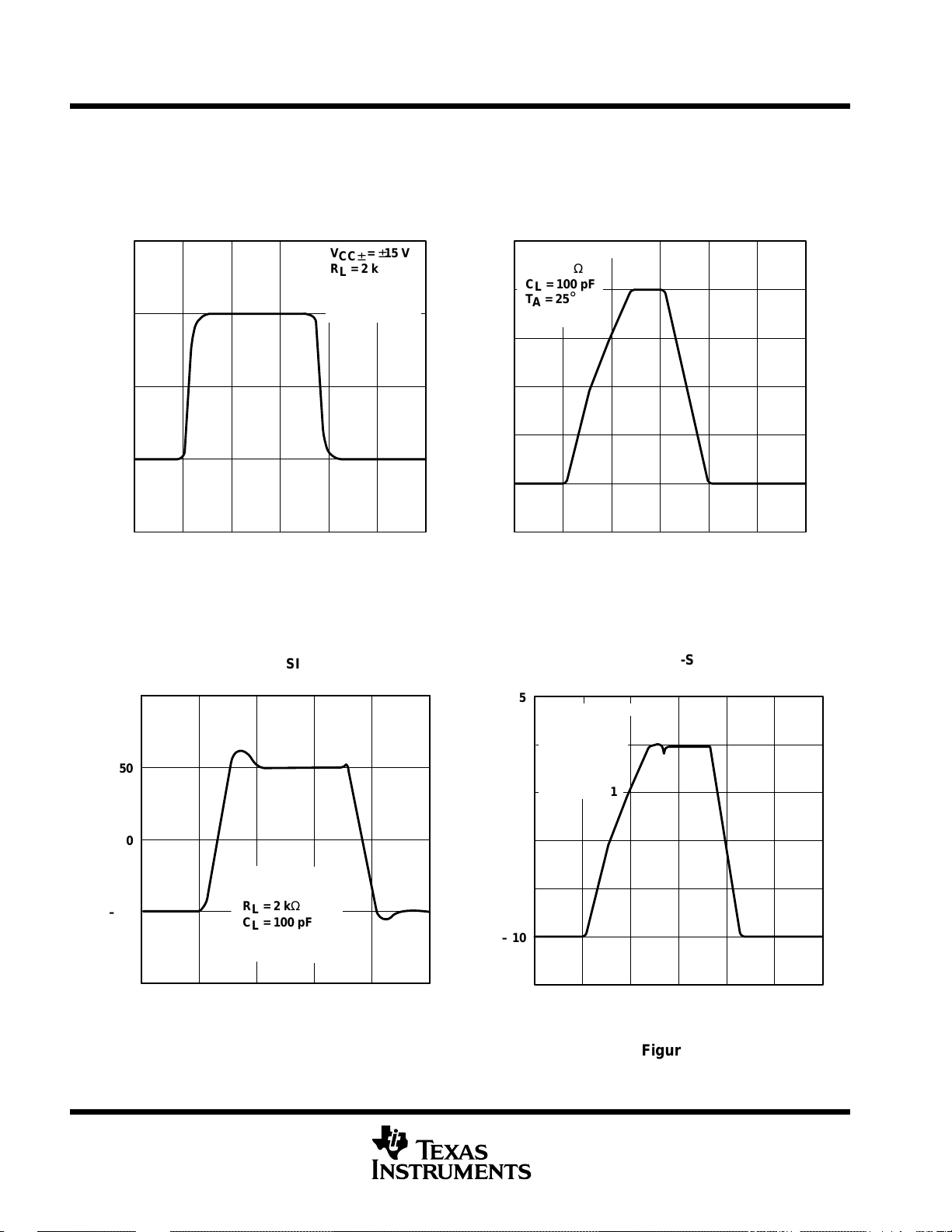
PARAMETER MEASUREMENT INFORMATION
R
f
15 V
–
R
I
+
V
I
– 15 V
NOTE A: CL includes fixture capacitance.
CL =
100 pF
(see Note A)
Figure 1. Slew-Rate Test Circuit Figure 2. Noise-Voltage Test Circuit
10 kΩ
100 Ω
V
I
15 V
–
+
–15 V
(see Note A)
CL =
100 pF
V
O
RL = 2 kΩ
V
O
2 kΩ
R
20 Ω
I
2 kΩ
15 V
–
V
O
+
– 15 V
20 Ω
R
f
15 V
–
V
O
+
V
I
– 15 V
NOTES: A. CL includes fixture capacitance.NOTE A: CL includes fixture capacitance.
B. For the TLE2037 and TLE2037A,
CL =
100 pF
(see Note A)
AVD must be ≥ 5.
2 kΩ
Figure 3. Unity-Gain Bandwidth and Figure 4. Small-Signal Pulse-
Phase-Margin Test Circuit (TLE2027 Only) Response Test Circuit
14
POST OFFICE BOX 655303 • DALLAS, TEXAS 75265

TLE2027, TLE2037, TLE2027A, TLE2037A, TLE2027Y, TLE2037Y
EXCALIBUR LOW-NOISE HIGH-SPEED
PRECISION OPERATIONAL AMPLIFIERS
SLOS192A – FEBRUARY 1997 REVISED MARCH 2002
typical values
Typical values presented in this data sheet represent the median (50% point) of device parametric performance.
initial estimates of parameter distributions
In the ongoing program of improving data sheets and supplying more information to our customers, Texas
Instruments has added an estimate of not only the typical values but also the spread around these values. These
are in the form of distribution bars that show the 95% (upper) points and the 5% (lower) points from the
characterization of the initial wafer lots of this new device type (see Figure 5). The distribution bars are shown
at the points where data was actually collected. The 95% and 5% points are used instead of ± 3 sigma since
some of the distributions are not true Gaussian distributions.
The number of units tested and the number of different wafer lots used are on all of the graphs where distribution
bars are shown. As noted in Figure 5, there were a total of 835 units from two wafer lots. In this case, there is
a good estimate for the within-lot variability and a possibly poor estimate of the lot-to-lot variability . This is always
the case on newly released products since there can only be data available from a few wafer lots.
The distribution bars are not intended to replace the minimum and maximum limits in the electrical tables. Each
distribution bar represents 90% of the total units tested at a specific temperature. While 10% of the units tested
fell outside any given distribution bar, this should not be interpreted to mean that the same individual devices
fell outside every distribution bar.
4.5
3.5
– Supply Current – mA
CC
I
2.5
SUPPLY CURRENT
FREE-AIR TEMPERATURE
5
V
= ±15 V
CC
±
VO = 0
No Load
Sample Size = 835 Units
From 2 Water Lots
4
3
TA – Free-Air Temperature –
Figure 5. Sample Graph With Distribution Bars
vs
95% point on the distribution bar
(5% of the devices fell above this point.)
90% of the devices were within the upper
and lower points on the distribution bar.
5% point on the distribution bar
(5% of the devices fell below this point.)
1501251007550250– 25– 50– 75
°C
POST OFFICE BOX 655303 • DALLAS, TEXAS 75265
15

TLE2027, TLE2037, TLE2027A, TLE2037A, TLE2027Y, TLE2037Y
IIBInput bias current
V
(g)
,
vsvsSu ly voltage
20
AVDLarge-signal differential voltage amplification
yg
,
OS
ICCSupply current
yg
Voltage-follower pulse response
g
,
B1Unity-gain bandwidth
yg
Gain bandwidth product
yg
φ
yg
,
φ
m
g
EXCALIBUR LOW-NOISE HIGH-SPEED
PRECISION OPERATIONAL AMPLIFIERS
SLOS192A – FEBRUARY 1997 REVISED MARCH 2002
TYPICAL CHARACTERISTICS
Table of Graphs
V
IO
∆V
I
IO
I
I
V
O(PP)
OM
z
o
CMRR Common-mode rejection ratio vs Frequency 28
k
SVR
I
OS
V
n
SR Slew rate vs Free-air temperature 48, 49
m
Input offset voltage Distribution 6, 7
Input offset voltage change vs Time after power on 8, 9
IO
Input offset current vs Free-air temperature 10
p
Input current vs Differential input voltage 13
Maximum peak-to-peak output voltage vs Frequency 14, 15
Maximum (positive/negative) peak output vs Load resistance 16, 17
voltage vs Free-air temperature
p
Output impedance vs Frequency 27
Supply-voltage rejection ratio vs Frequency 29
Short-circut output current
pp
p
Equivalent input noise voltage vs Frequency 42
Noise voltage (referred to input) Over 10-second interval 43
p
Phase margin
Phase shift vs Frequency 22 – 25
p
vs Free-air temperature 11
vs Common-mode input voltage 12
vs Supply voltage 20
Load resistance
vs Frequency 22 – 25
vs Free-air temperature 26
vs Supply voltage 30, 31
vs
Elapsed time
vs Free-air temperature 34, 35
vs Supply voltage 36
vs
Free-air temperature 37
Small signal 38, 40
Large signal
vs Supply voltage 44
vs
Load capacitance 45
vs Supply voltage 46
vs
Load capacitance 47
vs Supply voltage 50, 51
vs
Load capacitance
vs Free-air temperature 54, 55
FIGURE
18, 19
21
32, 33
39, 41
52, 53
16
POST OFFICE BOX 655303 • DALLAS, TEXAS 75265

DISTRIBUTION
INPUT OFFSET VOLTAGE
16
1568 Amplifiers Tested From 2 Wafer Lots
= +15 V
V
CC
14
12
10
8
6
±
TA = 25°C
D Package
TLE2027, TLE2037, TLE2027A, TLE2037A, TLE2027Y, TLE2037Y
EXCALIBUR LOW-NOISE HIGH-SPEED
PRECISION OPERATIONAL AMPLIFIERS
SLOS192A – FEBRUARY 1997 REVISED MARCH 2002
TYPICAL CHARACTERISTICS
INPUT OFFSET VOLTAGE CHANGE
TIME AFTER POWER ON
12
µV
10
8
6
vs
Percentage of Amplifiers – %
4
2
0
VIO – Input Offset Voltage – µV
0 120906030– 30– 60– 90– 120
Figure 6
INPUT OFFSET VOLTAGE CHANGE
vs
TIME AFTER POWER ON
6
µV
5
4
3
2
50 Amplifiers Tested From 2 Wafer Lots
= ±15 V
V
CC
1
IO
AVIO – Change in Input Offset Voltage –
∆V
0
0 20 40 60 80 100 120 140 160 180
±
TA = 25°C
P Package
t – Time After Power On – s
Figure 8
AVIO – Change in Input Offset Voltage –
∆V
IO
I
IIO – Input Offset Current – nA
IO
30
25
20
15
10
4
50 Amplifiers Tested From 2 Wafer Lots
V
2
0
0
= ±15 V
CC
±
TA = 25°C
D Package
10 20 30 40 50 60
t – Time After Power On – s
Figure 7
INPUT OFFSET CURRENT
vs
FREE-AIR TEMPERATURE
V
= ±15 V
CC
±
VIC = 0
Sample Size = 833 Units
From 2 Wafer Lots
5
0
– 75
TA – Free-Air Temperature – °C
Figure 9
†
1501251007550250– 25– 50
†
Data at high and low temperatures are applicable only within the rated operating free-air temperature ranges of the various devices.
POST OFFICE BOX 655303 • DALLAS, TEXAS 75265
17

TLE2027, TLE2037, TLE2027A, TLE2037A, TLE2027Y, TLE2037Y
EXCALIBUR LOW-NOISE HIGH-SPEED
PRECISION OPERATIONAL AMPLIFIERS
SLOS192A – FEBRUARY 1997 REVISED MARCH 2002
TYPICAL CHARACTERISTICS
IB
IIB – Input Bias Current – nA
I
0.8
0.6
60
50
40
30
20
10
–10
–20
1
INPUT BIAS CURRENT
†
vs
FREE-AIR TEMPERATURE
V
= ± 15 V
CC
±
VIC = 0
Sample Size = 836 Units
From 2 Wafer Lots
0
–75
–50 –25 0 25 50 75 100 125 150
TA – Free-Air Temperature – °C
Figure 10
INPUT CURRENT
DIFFERENTIAL INPUT VOLTAGE
V
= ± 15 V
CC
±
VIC = 0
TA = 25°C
vs
IB
IIB – Input Bias Current – nA
I
INPUT BIAS CURRENT
vs
COMMON-MODE INPUT VOLTAGE
40
= ± 15 V
V
CC
35
30
25
20
15
10
5
0
–12
±
TA = 25°C
– 8 – 40 4 812
VIC – Common-Mode Input Voltage – V
Figure 11
TLE2027
MAXIMUM PEAK-TO-PEAK
OUTPUT VOLTAGE
vs
FREQUENCY
30
25
†
V
= ±15 V
CC±
RL = 2 kΩ
0.4
0.2
0
– 0.2
– 0.4
I
II – Input Current – mA
I
– 0.6
– 0.8
– 1
– 1.8
– 1.2 – 0.6 0 0.6 1.2 1.8
VID – Differential Input Voltage – V
Figure 12
†
Data at high and low temperatures are applicable only within the rated operating free-air temperature ranges of the various devices.
18
POST OFFICE BOX 655303 • DALLAS, TEXAS 75265
– Maximum Peak-to-Peak Output Voltage – V
O(PP)
V
20
15
10
5
0
10 k
TA = 125
TA = – 55°C
f – Frequency – Hz
Figure 13
°C
10 M1 M100 k

TLE2027, TLE2037, TLE2027A, TLE2037A, TLE2027Y, TLE2037Y
ÁÁ
ÁÁ
EXCALIBUR LOW-NOISE HIGH-SPEED
PRECISION OPERATIONAL AMPLIFIERS
SLOS192A – FEBRUARY 1997 REVISED MARCH 2002
O(PP)
V
VO(PP) – Maximum Peak-to-Peak Output Voltage – V
30
25
20
15
10
5
0
– 14
– 12
– 10
10 k
TLE2037
TYPICAL CHARACTERISTICS
MAXIMUM PEAK-TO-PEAK
OUTPUT VOLTAGE
vs
FREQUENCY
TA = 125°C
TA = – 55°C
100 k 1 M 100 M
f – Frequency – Hz
Figure 14
MAXIMUM NEGATIVE PEAK
OUTPUT VOLTAGE
vs
LOAD RESISTANCE
†
V
= ± 15 V
CC
±
RL = 2 kΩ
10 M
MAXIMUM POSITIVE PEAK
OUTPUT VOLTAGE
vs
LOAD RESISTANCE
14
12
10
8
6
4
V
2
0
OM +
VOM+ – Maximum Positive Peak Output Voltage – V
100
V
= ± 15 V
CC
±
TA = 25°C
RL – Load Resistance – Ω
1 k 10 k
Figure 15
13.5
13.4
13.3
MAXIMUM POSITIVE PEAK
OUTPUT VOLTAGE
vs
FREE-AIR TEMPERATURE
V
= ± 15 V
CC
±
RL = 2 kΩ
Sample Size = 832 Units
From 2 Wafer Lots
†
– 8
13.2
– 6
13.1
– 4
VOM+ – Maximum Positive Peak Output Voltage – V
V
12.9
OM +
13
– 50 – 25 0 25 50 75 100 125 150
– 75
TA – Free-Air Temperature – °C
Figure 17
V
= ± 15 V
CC
– 2
0
OM –
VOM– – Maximum Negative Peak Output Voltage – V
100
V
±
TA = 25°C
1 k 10 k
RL – Load Resistance – Ω
Figure 16
†
Data at high and low temperatures are applicable only within the rated operating free-air temperature ranges of the various devices.
POST OFFICE BOX 655303 • DALLAS, TEXAS 75265
19

TLE2027, TLE2037, TLE2027A, TLE2037A, TLE2027Y, TLE2037Y
EXCALIBUR LOW-NOISE HIGH-SPEED
PRECISION OPERATIONAL AMPLIFIERS
SLOS192A – FEBRUARY 1997 REVISED MARCH 2002
TYPICAL CHARACTERISTICS
LARGE-SIGNAL DIFFERENTIAL
VOLTAGE AMPLIFICATION
TA = 25°C
– 13
– 13.2
MAXIMUM NEGATIVE PEAK
OUTPUT VOLTAGE
†
vs
FREE-AIR TEMPERATURE
V
= ± 15 V
CC
±
RL = 2 kΩ
Sample Size = 831 Units
From 2 Wafer Lots
50
Vµ
40
V/
SUPPLY VOLTAGE
vs
RL = 2 kΩ
RL = 1 kΩ
– 13.4
– 13.6
– 13.8
OM –
VOM– – Maximum Negative Peak Output Voltage – V
V
– 14
– 50 – 25 0 25 50 75 100 125 150
– 75
TA – Free-Air Temperature – °C
Figure 18
50
V
CC
±
TA = 25°C
Vµ
40
V/
30
20
Voltage Amplification –
VD
10
A
AVD – Large-Signal differential
0
0
LARGE-SIGNAL DIFFERENTIAL
VOLTAGE AMPLIFICATION
vs
LOAD RESISTANCE
= ± 15 V
RL = 600 Ω
4 8 12 16 20
V
– Supply Voltage – V
CC±
Figure 19
30
20
Voltage Amplification –
VD
A
AVD – Large-Signal differential
10
0
100 200 400 1 k 4 k 10 k2 k
RL – Load Resistance – Ω
Figure 20
†
Data at high and low temperatures are applicable only within the rated operating free-air temperature ranges of the various devices.
20
POST OFFICE BOX 655303 • DALLAS, TEXAS 75265

TLE2027, TLE2037, TLE2027A, TLE2037A, TLE2027Y, TLE2037Y
Á
Á
EXCALIBUR LOW-NOISE HIGH-SPEED
PRECISION OPERATIONAL AMPLIFIERS
SLOS192A – FEBRUARY 1997 REVISED MARCH 2002
TYPICAL CHARACTERISTICS
TLE2027
LARGE-SIGNAL DIFFERENTIAL VOLTAGE
AMPLIFICATION AND PHASE SHIFT
vs
FREQUENCY
160
75°
120
A
100
80
60
Voltage Amplification – dB
VD
40
A
AVD – Large-Signal Differential
20
0
0.1
V
CC±
RL = 2 kΩ
CL = 100 pF
TA = 25
VD
= ± 15 V
°C
LARGE-SIGNAL DIFFERENTIAL VOLTAGE
AMPLIFICATION AND PHASE SHIFT
160
Phase Shift
100 k100
f – Frequency – Hz
Figure 21
TLE2037
vs
FREQUENCY
100 M
100°140
125°
150°
175°
200°
225°
250°
275°
75°
Phase Shift
140
120
A
100
80
60
Voltage Amplification – dB
VD
A
AVD – Large-Signal Differential
V
40
20
CC
RL = 2 kΩ
CL = 100 pF
TA = 25°C
0
0.1
POST OFFICE BOX 655303 • DALLAS, TEXAS 75265
VD
= ± 15 V
±
Phase Shift
100 100 k
f – Frequency – MHz
Figure 22
100 M
100°
125°
150°
175°
200°
225°
250°
275°
Phase Shift
21

TLE2027, TLE2037, TLE2027A, TLE2037A, TLE2027Y, TLE2037Y
EXCALIBUR LOW-NOISE HIGH-SPEED
PRECISION OPERATIONAL AMPLIFIERS
SLOS192A – FEBRUARY 1997 REVISED MARCH 2002
TYPICAL CHARACTERISTICS
TLE2027
LARGE-SIGNAL DIFFERENTIAL VOLTAGE
AMPLIFICATION AND PHASE SHIFT
vs
FREQUENCY
6
100°
3
0
– 3
– 6
Phase Shift
– 9
– 12
Voltage Amplification – dB
VD
A
AVD – Large-Signal Differential
– 15
– 18
V
CC±
RL = 2 kΩ
CL = 100 pF
TA = 25
10
= ± 15 V
°C
LARGE-SIGNAL DIFFERENTIAL VOLTAGE
AMPLIFICATION AND PHASE SHIFT
30
f – Frequency – MHz
Figure 23
TLE2037
vs
FREQUENCY
125°
150°
100
175°
200°
225°
250°
275°
300°
100
Phase Shift
°
A
VD
704020
22
25
20
15
10
5
V
0
Voltage Amplification – dB
VD
A
AVD – Large-Signal Differential
RL = 2 kΩ
CL = 100 pF
– 5
TA = 25°C
–10
1 2 4 10 40 100
CC
A
VD
= ± 15 V
±
f – Frequency – MHz
Phase Shift
20
Figure 24
POST OFFICE BOX 655303 • DALLAS, TEXAS 75265
125
150
175
200
225
250
275
300
°
°
°
°
Phase Shift
°
°
°
°

TLE2027, TLE2037, TLE2027A, TLE2037A, TLE2027Y, TLE2037Y
EXCALIBUR LOW-NOISE HIGH-SPEED
PRECISION OPERATIONAL AMPLIFIERS
SLOS192A – FEBRUARY 1997 REVISED MARCH 2002
TYPICAL CHARACTERISTICS
LARGE-SIGNAL DIFFERENTIAL
VOLTAGE AMPLIFICATION
FREE-AIR TEMPERATURE
60
V
= ± 15 V
CC ±
Vµ
V/
50
40
Voltage Amplification –
VD
A
AVD – Large-Signal differential
30
–75
–50 –25 0 25 50 75 100 125
TA – Free-Air Temperature – °C
vs
Figure 25
†
RL = 2 kΩ
RL = 1 kΩ
150
OUTPUT IMPEDANCE
vs
FREQUENCY
100
V
= ± 15 V
CC ±
TA = 25°C
Ω
10
AVD = 100
1
AVD = 10
o
z
zo – Output Impedance –
–10
–100
10
100 1 k 10 k 100 k 1 M 10 M
f – Frequency – Hz
NOTE A: For this curve, the TLE2027 is AVD = 1 and the
TLE2037 is AVD = 5.
See Note A
100 M
Figure 26
COMMON-MODE REJECTION RATIO
vs
FREQUENCY
– Supply-Voltage Rejection Ratio – dB
SVR
K
140
120
100
140
120
100
CMRR – Common-Mode Rejection Ratio – dB
80
60
40
20
V
= ± 15 V
CC ±
TA = 25°C
0
10
100 1 k 10 k 100 k 1 M 10 M
f – Frequency – Hz
100 M
Figure 27
†
Data at high and low temperatures are applicable only within the rated operating free-air temperature ranges of the various devices.
SUPPLY-VOLTAGE REJECTION RATIO
vs
FREQUENCY
V
TA = 25°C
k
SVR–
80
60
k
40
20
0
10
100 1 k 10 k 100 k 1 M 10 M
SVR+
f – Frequency – Hz
Figure 28
CC ±
= ± 15 V
100 M
POST OFFICE BOX 655303 • DALLAS, TEXAS 75265
23

TLE2027, TLE2037, TLE2027A, TLE2037A, TLE2027Y, TLE2037Y
БББББ
БББББ
БББББ
EXCALIBUR LOW-NOISE HIGH-SPEED
PRECISION OPERATIONAL AMPLIFIERS
SLOS192A – FEBRUARY 1997 REVISED MARCH 2002
TYPICAL CHARACTERISTICS
OS
IOS – Short-Circuit Output Current – mA
I
– 45
– 43
–42
–40
–38
–36
–34
–32
–30
SHORT-CIRCUIT OUTPUT CURRENT
vs
SUPPLY VOLTAGE
VID = 100 mV
VO = 0
TA = 25°C
P Package
0
2 4 6 8 10 12 14 16 18 20
V
– Supply Voltage – V
CC±
Figure 29
SHORT-CIRCUIT OUTPUT CURRENT
vs
ELAPSED TIME
V
= ± 15 V
CC ±
VID = 100 mV
VO = 0
TA = 25°C
P Package
OS
IOS – Short-Circuit Output Current – mA
I
44
42
44
42
40
38
36
34
32
30
0
SHORT-CIRCUIT OUTPUT CURRENT
vs
SUPPLY VOLTAGE
VID = – 100 mV
VO = 0
TA = 25°C
P Package
2 4 6 8 10 12 14 16 18 20
V
– Supply Voltage – V
CC±
Figure 30
SHORT-CIRCUIT OUTPUT CURRENT
vs
ELAPSED TIME
V
= ± 15 V
CC ±
VID = 100 mV
VO = 0
TA = 25°C
P Package
– 41
– 39
– 37
OS
IOS – Short-Circuit Output Current – mA
I
– 35
24
0
30 60 90 120 150
t – Elasped Time – s
Figure 31
40
38
36
OS
IOS – Short-Circuit Output Current – mA
I
180
POST OFFICE BOX 655303 • DALLAS, TEXAS 75265
34
0
30 60 90 120 150
t – Elasped Time – s
Figure 32
180

TLE2027, TLE2037, TLE2027A, TLE2037A, TLE2027Y, TLE2037Y
ÁÁ
EXCALIBUR LOW-NOISE HIGH-SPEED
PRECISION OPERATIONAL AMPLIFIERS
SLOS192A – FEBRUARY 1997 REVISED MARCH 2002
TYPICAL CHARACTERISTICS
OS
IOS – Short-Circuit Output Current – mA
I
ICC – Supply Current – mA
I
– 48
– 44
– 40
– 36
– 32
– 28
– 24
CC
SHORT-CIRCUIT OUTPUT CURRENT
vs
FREE-AIR TEMPERATURE
– 75
– 50 – 25 0 25 50 75 100 125
TA – Free-Air Temperature – °C
Figure 33
SUPPLY CURRENT
SUPPLY VOLTAGE
6
VO = 0
No Load
5
4
3
2
1
vs
V
= ± 15 V
CC ±
VID = 100 mV
VO = 0
P Package
†
TA = 125°C
TA = 25°C
TA = – 55°C
†
SHORT-CIRCUIT OUTPUT CURRENT
†
vs
FREE-AIR TEMPERATURE
46
V
= ± 15 V
CC ±
VID = –100 mV
VO = 0
P Package
1251007550250– 25– 50 150– 75
150
OS
IOS – Short-Circuit Output Current – mA
I
42
38
34
30
26
TA – Free-Air Temperature – °C
Figure 34
†
CC
ICC – Supply Current – mA
I
FREE-AIR TEMPERATURE
5
V
= ± 15 V
CC ±
VO = 0
No Load
4.5
Sample Size = 836 Units
From 2 Wafer Lots
4
3.5
3
SUPPLY CURRENT
vs
0
0
2 4 6 8 10 12 14 16 18 20
V
– Supply Voltage – V
CC
±
Figure 35
†
Data at high and low temperatures are applicable only within the rated operating free-air temperature ranges of the various devices.
POST OFFICE BOX 655303 • DALLAS, TEXAS 75265
2.5
– 75
– 50 – 25 0255075 100 125
TA – Free-Air Temperature – °C
Figure 36
150
25
TLE2027, TLE2037, TLE2027A, TLE2037A, TLE2027Y, TLE2037Y
EXCALIBUR LOW-NOISE HIGH-SPEED
PRECISION OPERATIONAL AMPLIFIERS
SLOS192A – FEBRUARY 1997 REVISED MARCH 2002
TYPICAL CHARACTERISTICS
– Output Voltage – mV
O
V
– 50
– 100
100
50
TLE2027
VOLTAGE-FOLLOWER
VOLTAGE-FOLLOWER
SMALL-SIGNAL
PULSE RESPONSE
V
= ±15 V
CC±
RL = 2 kΩ
CL = 100 pF
°C
TA = 25
See Figure 4
0
1000
8006004002000
t – Time – ns
15
V
= ±15 V
CC±
RL = 2 kΩ
CL = 100 pF
10
5
0
– Output Voltage – V
– 5
O
V
– 10
– 15
°C
TA = 25
See Figure 1
Figure 37
TLE2027
LARGE-SIGNAL
PULSE RESPONSE
250 5 10 15 20
t – Time – µs
Figure 38
O
VO – Output Voltage – mV
V
– 100
100
50
– 50
TLE2037
VOLTAGE-FOLLOWER
VOLTAGE-FOLLOWER
SMALL-SIGNAL
PULSE RESPONSE
15
V
= ± 15 V
CC ±
AVD = 5
RL = 2 kΩ
10
CL = 100 pF
TA = 25°C
See Figure 1
5
0
V
= ± 15 V
CC ±
AVD = 5
RL = 2 kΩ
CL = 100 pF
TA = 25°C
See Figure 4
2001000
t – Time – ns
300
400
0
– 5
O
VO – Output Voltage – V
V
– 10
– 15
Figure 39
TLE2037
LARGE-SIGNAL
PULSE RESPONSE
8642010
t – Time – µs
Figure 40
26
POST OFFICE BOX 655303 • DALLAS, TEXAS 75265

TLE2027, TLE2037, TLE2027A, TLE2037A, TLE2027Y, TLE2037Y
БББББББ
БББББББ
БББББББ
БББББББ
EXCALIBUR LOW-NOISE HIGH-SPEED
PRECISION OPERATIONAL AMPLIFIERS
SLOS192A – FEBRUARY 1997 REVISED MARCH 2002
TYPICAL CHARACTERISTICS
10
nV/ Hz
8
6
4
2
n
V
Vn – Equivalent Input Noise Voltage – nVHz
0
EQUIVALENT INPUT NOISE VOLTAGE
vs
FREQUENCY
V
= ± 15 V
CC ±
RS = 20 Ω
TA = 25°C
See Figure 2
Sample Size = 100 Units
From 2 Wafer Lots
1
10 100 1 k 10 k
f – Frequency – Hz
Figure 41
100 k
Noise Voltage – nV
50
40
30
20
10
– 10
– 20
– 30
– 40
– 50
0
0
NOISE VOLTAGE
(REFERRED TO INPUT)
OVER A
V
= ± 15 V
CC ±
f = 0.1 to 10 Hz
TA = 25°C
10-SECOND INTERVAL
246 8
t – Time – s
Figure 42
10
20
18
16
14
– Unity-Gain Bandwidth – MHz
12
1
B
10
RL = 2 kΩ
CL = 100 pF
TA = 25
See Figure 3
0
TLE2027
UNITY-GAIN BANDWIDTH
vs
SUPPLY VOLTAGE
°C
| V
| – Supply Voltage – V
CC
±
Figure 43
TLE2037
GAIN-BANDWIDTH PRODUCT
vs
SUPPLY VOLTAGE
52
f = 100 kHz
RL = 2 kΩ
CL = 100 pF
TA = 25°C
51
50
49
Gain-Bandwidth Product – MHz
48
0
201816141210864222
2 468 10 12 14 16 18 20
V
– Supply Voltage – V
CC±
Figure 44
POST OFFICE BOX 655303 • DALLAS, TEXAS 75265
27

TLE2027, TLE2037, TLE2027A, TLE2037A, TLE2027Y, TLE2037Y
EXCALIBUR LOW-NOISE HIGH-SPEED
PRECISION OPERATIONAL AMPLIFIERS
SLOS192A – FEBRUARY 1997 REVISED MARCH 2002
TYPICAL CHARACTERISTICS
TLE2027
UNITY-GAIN BANDWIDTH
16
12
vs
LOAD CAPACITANCE
V
= ±15 V
CC±
RL = 2 kΩ
TA = 25°C
See Figure 3
52
51
GAIN-BANDWIDTH PRODUCT
TLE2037
vs
LOAD CAPACITANCE
V
= ±15 V
CC±
RL = 2 kΩ
TA = 25°C
– Unity-Gain Bandwidth – MHz
1
B
2.8
µ
2.6
3
8
4
0
100
1000
CL – Load Capacitance – pF
Figure 45
TLE2027
SLEW RATE
FREE-AIR TEMPERATURE
†
vs
10000
sµ
50
49
Gain-Bandwidth Product – MHz
48
10
9
8
100
FREE-AIR TEMPERATURE
V
= ± 15 V
CC ±
AVD = 5
RL = 2 kΩ
CL = 100 pF
See Figure 1
1000
CL – Load Capacitance – pF
Figure 46
TLE2037
SLEW RATE
†
vs
10000
2.4
SR – Slew Rate – V/ s
V
= ±15 V
CC±
AVD = 1
2.2
RL = 2 kΩ
CL = 100 pF
See Figure 1
2
– 75
TA – Free-Air Temperature – °C
1251007550250– 25– 50
150
Figure 47
†
Data at high and low temperatures are applicable only within the rated operating free-air temperature ranges of the various devices.
28
POST OFFICE BOX 655303 • DALLAS, TEXAS 75265
SR – Slew Rate – V/
7
6
5
– 75
– 50 – 25 0 25 50 75 100 125
TA – Free-Air Temperature – °C
Figure 48
150

TLE2027, TLE2037, TLE2027A, TLE2037A, TLE2027Y, TLE2037Y
EXCALIBUR LOW-NOISE HIGH-SPEED
PRECISION OPERATIONAL AMPLIFIERS
SLOS192A – FEBRUARY 1997 REVISED MARCH 2002
TYPICAL CHARACTERISTICS
58°
RL = 2 kΩ
CL = 100 pF
56°
TA = 25
See Figure 3
54°
52°
50°
48°
– Phase Margin
m
φ
46°
44°
42°
0
TLE2027
PHASE MARGIN
SUPPLY VOLTAGE
°C
| – Supply Voltage – V
| V
CC
±
Figure 49
vs
TLE2037
PHASE MARGIN
vs
SUPPLY VOLTAGE
52°
AVD = 5
RL = 2 kΩ
50°
CL = 100 pF
TA = 25°C
48°
46°
44°
– Phase Margin
m
φ
42°
40°
38°
0
2018161412108642
22
2 468 10 12 14 16 18 20
V
– Supply Voltage – V
CC±
Figure 50
60°
50°
40°
30°
– Phase Margin
m
20°
φ
10°
0°
100
TLE2027
PHASE MARGIN
vs
LOAD CAPACITANCE
V
CC±
RL = 2 kΩ
TA = 25°C
See Figure 3
1000
CL – Load Capacitance – pF
Figure 51
= ±15 V
60°
50°
40°
30°
20°
m
φ – Phase Margin
10°
0°
100
TLE2037
PHASE MARGIN
vs
LOAD CAPACITANCE
V
CC ±
RL = 2 kΩ
TA = 25
1000
CL – Load Capacitance – pF
Figure 52
= ± 15 V
°C
10000
POST OFFICE BOX 655303 • DALLAS, TEXAS 75265
29

TLE2027, TLE2037, TLE2027A, TLE2037A, TLE2027Y, TLE2037Y
EXCALIBUR LOW-NOISE HIGH-SPEED
PRECISION OPERATIONAL AMPLIFIERS
SLOS192A – FEBRUARY 1997 REVISED MARCH 2002
TYPICAL CHARACTERISTICS
TLE2027
PHASE MARGIN
†
vs
65°
60°
55°
50°
– Phase Margin
m
45°
φ
40°
35°
– 75
FREE-AIR TEMPERATURE
V
CC±
RL = 2 kΩ
TA = 25
See Figure 3
TA – Free-Air Temperature –
= ±15 V
°C
°C
55°
53°
51°
49°
m
φ – Phase Margin
47°
45°
150
1251007550250– 25– 50
– 75
FREE-AIR TEMPERATURE
TA – Free-Air Temperature – °C
Figure 53
†
Data at high and low temperatures are applicable only within the rated operating free-air temperature ranges of the various devices.
TLE2037
PHASE MARGIN
vs
Figure 54
†
V
= ± 15 V
CC ±
AVD = 5
RL = 2 kΩ
CL = 100 pF
150– 50 – 25 0 25 50 75 100 125
30
POST OFFICE BOX 655303 • DALLAS, TEXAS 75265
TLE2027, TLE2037, TLE2027A, TLE2037A, TLE2027Y, TLE2037Y
EXCALIBUR LOW-NOISE HIGH-SPEED
PRECISION OPERATIONAL AMPLIFIERS
SLOS192A – FEBRUARY 1997 REVISED MARCH 2002
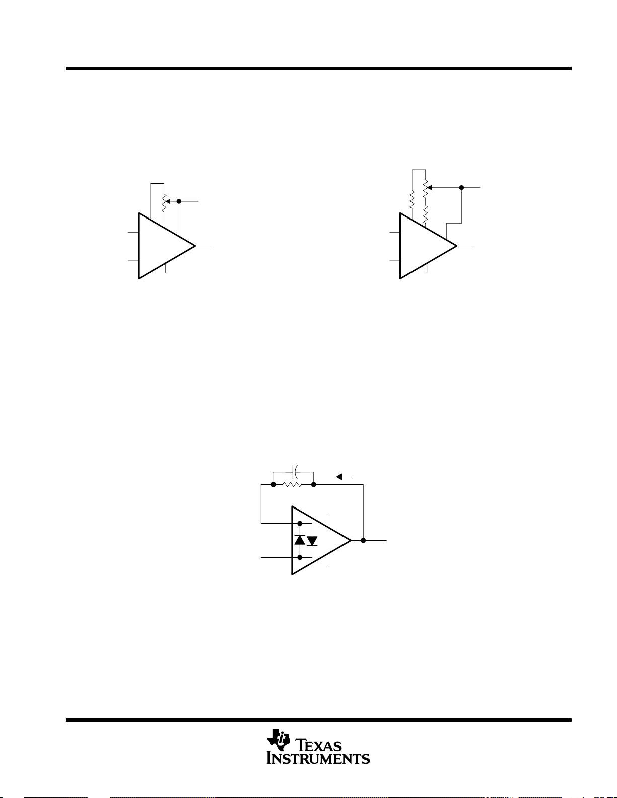
APPLICATION INFORMATION
input offset voltage nulling
The TLE2027 and TLE2037 series offers external null pins that can be used to further reduce the input offset
voltage. The circuits of Figure 55 can be connected as shown if the feature is desired. If external nulling is not
needed, the null pins may be left disconnected.
1 kΩ
10 kΩ
IN –
IN +
(a) STANDARD ADJUSTMENT (b) ADJUSTMENT WITH IMPROVED SENSITIVITY
–
+
V
CC –
V
CC +
OUT
IN –
IN +
4.7 kΩ
4.7 kΩ
–
+
V
CC –
V
CC +
OUT
Figure 55. Input Offset Voltage Nulling Circuits
voltage-follower applications
The TLE2027 circuitry includes input-protection diodes to limit the voltage across the input transistors; however,
no provision is made in the circuit to limit the current if these diodes are forward biased. This condition can occur
when the device is operated in the voltage-follower configuration and driven with a fast, large-signal pulse. It
is recommended that a feedback resistor be used to limit the current to a maximum of 1 mA to prevent
degradation of the device. Also, this feedback resistor forms a pole with the input capacitance of the device.
For feedback resistor values greater than 10 kΩ, this pole degrades the amplifier phase margin. This problem
can be alleviated by adding a capacitor (20 pF to 50 pF) in parallel with the feedback resistor (see Figure 56).
CF = 20 to 50 pF
IF
R
F
V
CC
–
V
I
+
V
CC–
Figure 56. Voltage Follower
≤ 1 mA
V
O
POST OFFICE BOX 655303 • DALLAS, TEXAS 75265
31

TLE2027, TLE2037, TLE2027A, TLE2037A, TLE2027Y, TLE2037Y
EXCALIBUR LOW-NOISE HIGH-SPEED
PRECISION OPERATIONAL AMPLIFIERS
SLOS192A – FEBRUARY 1997 REVISED MARCH 2002
APPLICATION INFORMATION
macromodel information
Macromodel information provided was derived using Microsim Parts, the model generation software used
with Microsim PSpice . The Boyle macromodel (see Note 6) and subcircuit in Figure 57, Figure 58, and
Figure 59 were generated using the TLE20x7 typical electrical and operating characteristics at 25°C. Using this
information, output simulations of the following key parameters can be generated to a tolerance of 20% (in most
cases):
• Maximum positive output voltage swing
• Maximum negative output voltage swing
• Slew rate
• Quiescent power dissipation
• Input bias current
• Open-loop voltage amplification
NOTE 6: G. R. Boyle, B. M. Cohn, D. O. Pederson, and J. E. Solomon, “Macromodeling of Integrated Circuit Operational Amplifiers”, IEEE Journal
of Solid-State Circuits, SC-9, 353 (1974).
V
CC +
rc1
c1
11
13
re1 re2
14
lee
4
V
IN +
IN –
CC –
rp
1
2
dp
3
rc2
12
Q2Q1
ree
cee
10
54
– +
ve
+
vc
–
53
dc
de
9
r2
6
gcm
• Gain-bandwidth product
• Common-mode rejection ratio
• Phase margin
• DC output resistance
• AC output resistance
• Short-circuit output current limit
99
vb
+
fb
–
C2
ga
7
vlim
ro2
hlim
8
OUT
90
+ dip
–
+
–
ro1
5
egnd
+
–
dln
92
91
vip
–
vin
+
+
–
Figure 57. Boyle Macromodel
PSpice and Parts are trademarks of MicroSim Corporation.
32
POST OFFICE BOX 655303 • DALLAS, TEXAS 75265

TLE2027, TLE2037, TLE2027A, TLE2037A, TLE2027Y, TLE2037Y
APPLICATION INFORMATION
macromodel information (continued)
EXCALIBUR LOW-NOISE HIGH-SPEED
PRECISION OPERATIONAL AMPLIFIERS
SLOS192A – FEBRUARY 1997 REVISED MARCH 2002
.subckt TLE2027 1 2 3 4 5
*
c1 11 12 4.003E-12
c2 6 7 20.00E-12
dc 5 53 dz
de 54 5 dz
dlp 90 91 dz
dln 92 90 dx
dp 4 3 dz
egnd 99 0 poly(2) (3,0)
(4,0) 0 5 .5
fb 7 99 poly(5) vb vc
ve vlp vln 0 954.8E6 –1E9 1E9 1E9
–1E9
ga 6 0 11 12
2.062E-3
gcm 0 6 10 99
531.3E-12
iee 10 4 dc 56.01E-6
hlim 90 0 vlim 1K
q1 11 2 13 qx
Figure 58. TLE2027 Macromodel Subcircuit
.subckt TLE2037 1 2 3 4 5
*
c1 11 12 4.003E–12
c2 6 7 7.500E–12
dc 5 53 dz
de 54 5 dz
dlp 90 91 dz
dln 92 90 dx
dp 4 3 dz
egnd 99 0 poly(2) (3,0)
(4,0) 0 .5 .5
fb 7 99 poly(5) vb vc
ve vip vln 0 923.4E6 A800E6
800E6 800E6 A800E6
ga 6 0 11 12 2.121E–3
gcm 0 6 10 99 597.7E–12
iee 10 4 dc 56.26E–6
hlim 90 0 vlim 1K
q1 11 2 13 qx
q2 12 1 14 qx
r2 6 9 100.0E3
rc1 3 11 530.5
rc2 3 12 530.5
re1 13 10 –393.2
re2 14 10 –393.2
ree 10 99 3.571E6
ro1 8 5 25
ro2 7 99 25
rp 3 4 8.013E3
vb 9 0 dc 0
vc 3 53 dc 2.400
ve 54 4 dc 2.100
vlim 7 8 dc 0
vlp 91 0 dc 40
vln 0 92 dc 40
.modeldx D(Is=800.0E-18)
.modelqx NPN(Is=800.0E-18
Bf=7.000E3)
.ends
q2 12 1 14 qz
r2 6 9 100.0E3
rc1 3 11 471.5
rc2 3 12 471.5
re1 13 10 A448
re2 14 10 A448
ree 10 99 3.555E6
ro1 8 5 25
ro2 7 99 25
rp 3 4 8.013E3
vb 9 0 dc 0
vc 3 53 dc 2.400
ve 54 4 dc 2.100
vlim 7 8 dc 0
vlp 91 0 dc 40
vln 0 92 dc 40
.model dxD(Is=800.0E–18)
.model qxNPN(Is=800.0E–18
Bf=7.031E3)
.ends
Figure 59. TLE2037 Macromodel Subcircuit
POST OFFICE BOX 655303 • DALLAS, TEXAS 75265
33

TLE2027, TLE2037, TLE2027A, TLE2037A, TLE2027Y, TLE2037Y
EXCALIBUR LOW-NOISE HIGH-SPEED
PRECISION OPERATIONAL AMPLIFIERS
SLOS192A – FEBRUARY 1997 REVISED MARCH 2002
34
POST OFFICE BOX 655303 • DALLAS, TEXAS 75265

IMPORTANT NOTICE
Texas Instruments Incorporated and its subsidiaries (TI) reserve the right to make corrections, modifications,
enhancements, improvements, and other changes to its products and services at any time and to discontinue
any product or service without notice. Customers should obtain the latest relevant information before placing
orders and should verify that such information is current and complete. All products are sold subject to TI’s terms
and conditions of sale supplied at the time of order acknowledgment.
TI warrants performance of its hardware products to the specifications applicable at the time of sale in
accordance with TI’s standard warranty . Testing and other quality control techniques are used to the extent TI
deems necessary to support this warranty . Except where mandated by government requirements, testing of all
parameters of each product is not necessarily performed.
TI assumes no liability for applications assistance or customer product design. Customers are responsible for
their products and applications using TI components. T o minimize the risks associated with customer products
and applications, customers should provide adequate design and operating safeguards.
TI does not warrant or represent that any license, either express or implied, is granted under any TI patent right,
copyright, mask work right, or other TI intellectual property right relating to any combination, machine, or process
in which TI products or services are used. Information published by TI regarding third–party products or services
does not constitute a license from TI to use such products or services or a warranty or endorsement thereof.
Use of such information may require a license from a third party under the patents or other intellectual property
of the third party , or a license from TI under the patents or other intellectual property of TI.
Reproduction of information in TI data books or data sheets is permissible only if reproduction is without
alteration and is accompanied by all associated warranties, conditions, limitations, and notices. Reproduction
of this information with alteration is an unfair and deceptive business practice. TI is not responsible or liable for
such altered documentation.
Resale of TI products or services with statements different from or beyond the parameters stated by TI for that
product or service voids all express and any implied warranties for the associated TI product or service and
is an unfair and deceptive business practice. TI is not responsible or liable for any such statements.
Mailing Address:
Texas Instruments
Post Office Box 655303
Dallas, Texas 75265
Copyright 2002, Texas Instruments Incorporated
 Loading...