www.ti.com
On/Off
Input
Shift
Register
DC Input
Shift
Register
7−bit DC
Delay
x0
Constant
Driver
MODE
0 1
MODE
0
1
0
15
111
0
0
6
0
0
1
7−bit DC
Constant
Driver
7
13
1
7−bit DC
Constant
Driver
On/Off
105
111
15
Maximum
OUTn Current
GNDVCC SINSCLK
SOUT
XLATMODE
OUT0
OUT1
OUT15
PGND BLANK
BLANK
16
112
Delay
x1
Delay
x15
IREF
Current
BLANK
Current
Current
Register
Register
Register
On/Off
Register
Register
On/Off
Register
TLC5922
SLVS486A – SEPTEMBER 2003 – REVISED MARCH 2005
LED DRIVER
FEATURES
• Controlled In-Rush Current
• 16 Channels
• Drive Capability
– 0 to 80 mA (Constant-Current Sink)
• Constant Current Accuracy
– ±1% (typical)
APPLICATIONS
• Monocolor, Multicolor, Fullcolor LED Display
• Monocolor, Multicolor LED Signboard
• Display Backlighting
• Multicolor LED Lighting Applications
• Serial Data Interface, SPI Compatible
• Fast Switching Output: Tr/ Tf= 10ns (typical)
• CMOS Level Input/Output
DESCRIPTION
The TLC5922 is a 16-channel constant-current sink
• 30 MHz Data Transfer Rate driver. Each channel has an On/Off state and a
• V
= 3.0 V to 5.5 V
CC
• Operating Temperature = –20 °C to 85 °C
• LED Supply Voltage up to 17 V
• 32-pin HTSSOP ( PowerPAD™) Package
• Dot Correction
128-step adjustable constant-current sink (dot correction). The dot correction adjusts the brightness variations between LED, LED channels, and other LED
drivers. Both dot correction and On/Off state are
accessible via a serial data interface. A single external resistor sets the maximum current of all 16
channels.
– 7 bit (128 Steps)
– Individually Adjustable For Each Channel
Please be aware that an important notice concerning availability, standard warranty, and use in critical applications of Texas
Instruments semiconductor products and disclaimers thereto appears at the end of this data sheet.
PowerPAD is a trademark of Texas Instruments.
PRODUCTION DATA information is current as of publication date.
Products conform to specifications per the terms of the Texas
Instruments standard warranty. Production processing does not
necessarily include testing of all parameters.
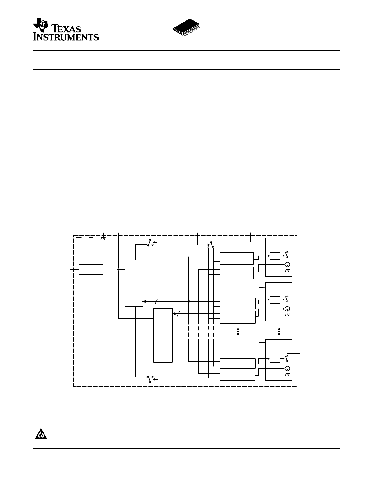
Figure 1. Functional Block Diagram
Copyright © 2003–2005, Texas Instruments Incorporated

www.ti.com
TLC5922
SLVS486A – SEPTEMBER 2003 – REVISED MARCH 2005
These devices have limited built-in ESD protection. The leads should be shorted together or the device
placed in conductive foam during storage or handling to prevent electrostatic damage to the MOS gates.
ORDERING INFORMATION
T
A
Package Part Number
(1)
(2)
–20 °C to 85 °C 4 mm x 4 mm, 32-pin HTSSOP TLC5922DAP
(1) For the most current package and ordering information, see the Package Option Addendum at the
end of this document, or see the TI website at www.ti.com .
(2) The DAP package is available in tape and reel. Add R suffix (TLC5922DAPR) to order quantities of
2000 parts per reel.
ABSOLUTE MAXIMUM RATINGS
(1) (2)
TLC5922 UNIT
V
CC
I
O
V
I
V
O
Supply voltage
Output current (dc) I
Input voltage range
Output voltage range
ESD rating
T
stg
Storage temperature range –40 to 150 °C
(2)
(2)
(2)
L(LC)
V
, V
, V
, V
(BLANK)
V
(SOUT)
V
(OUT0)
(XLAT)
(SCLK)
– V
(OUT15)
, V
(SIN)
(MODE)
HBM (JEDEC JESD22-A114, Human Body
Model)
CDM (JEDEC JESD22-C101, Charged Device
Model)
–0.3 to 6 V
90 mA
–0.3 to V
–0.3 to V
+ 0.3 V
CC
+ 0.3 V
CC
–0.3 to 18 V
2 kV
500 V
Continuous total power dissipation at (or below) TA= 25°C 3.9 W
Power dissipation rating at (or above) TA= 25°C 31.4 mW/°C
(1) Stresses beyond those listed under "absolute maximum ratings" may cause permanent damage to the device. These are stress ratings
only, and functional operation of the device at these or any other conditions beyond those indicated under "recommended operating
conditions" is not implied. Exposure to absolute-maximum-rated conditions for extended periods may affect device reliability.
(2) All voltage values are with respect to network ground terminal.
RECOMMENDED OPERATING CONDITIONS DC Characteristics
V
CC
V
O
V
IH
V
IL
I
OH
I
OL
I
OLC
T
A
(1) Please contact TI sales for slightly extended temperature range.
2
Supply voltage 3 5.5 V
Voltage applied to output, (Out0 - Out15) 17 V
High-level input voltage 0.8 VCC VCC V
Low-level input voltage GND 0.2 VCC V
High-level output current V
Low-level output current V
Constant output current OUT0 to OUT15 80 mA
Operating free-air temperature range
(1)
MIN NOM MAX UNIT
= 5 V at SOUT –1 mA
CC
= 5 V at SOUT 1 mA
CC
–20 85 °C

www.ti.com
SLVS486A – SEPTEMBER 2003 – REVISED MARCH 2005
AC Characteristics
V
= 3 V to 5.5 V, TA= –20°C to 85°C (unless otherwise noted)
CC
MIN TYP MAX UNIT
f
SCLK
t
wh0
t
wh1
t
su0
t
su1
t
su2
t
su3
t
h0
t
h1
t
h2
t
h3
Clock frequency SCLK 30 MHz
/t
CLK pulse duration SCLK = H/L 16 ns
wl0
XLAT pulse duration XLAT = H 20 ns
SIN – SCLK ↑ 10 ns
Setup time
SCLK ↑ – XLAT ↓ 10 ns
MODE ↑ ↓ – SCLK ↑ 10 ns
MODE ↑ ↓ – XLAT ↓ 10 ns
SCLK ↑ – SIN 10 ns
Hold time
XLAT ↓ – SCLK ↑ 10 ns
SCLK ↑ – MODE ↑ ↓ 10 ns
XLAT ↓ – MODE ↑ ↓ 10 ns
ELECTRICAL CHARACTERISTICS
V
= 3 V to 5.5 V, TA= –20°C to 85°C (unless otherwise noted)
CC
PARAMETER TEST CONDITIONS MIN TYP MAX UNIT
V
OH
V
OL
I
I
I
CC
I
OLC
I
LO0
∆ I
OLC0
∆ I
OLC1
∆ I
OLC2
∆ I
OLC3
V
(IREF)
(1) Measured at device start-up temperature. Once the IC is operating (self heating), lower ICCvalues are seen. See Figure 12 .
High-level output voltage IOH= –1 mA, SOUT V
–0.5 V
CC
Low-level output voltage IOL= 1 mA, SOUT 0.5 V
Input current –1 1 µA
VI= V
MODE
or GND, BLANK, XLAT, SCLK, SIN,
CC
No data transfer, All output OFF, VO= 1 V,
R
= 10 k Ω
(IREF)
No data transfer, All output OFF, VO= 1 V,
R
= 1.3 k Ω
Supply current mA
Constant output current All output ON, VO= 1 V, R
Leakage output current 0.1 µA
Constant current error ± 1 ± 4 %
Constant current error ± 4 ± 8.5 %
Power supply rejection ratio ± 1 ± 4 %/V
Load regulation Ω , ± 2 ± 6 %/V
(IREF)
Data transfer 30 MHz, All output ON, VO= 1 V,
R
= 1.3 k Ω
(IREF)
Data transfer 30 MHz, All output ON, VO= 1 V,
R
= 600 k Ω
(IREF)
= 600 Ω 70 80 90 mA
(IREF)
All output OFF, VO= 15 V, R
OUT0 to OUT15
All output ON, VO= 1 V, R
OUT0 to OUT15
= 600 Ω ,
(IREF)
= 600 Ω ,
(IREF)
device to device, averaged current from OUT0
to OUT15, R
All output ON, VO= 1 V, R
OUT0 to OUT15
All output ON, VO= 1 V to 3 V, R
= 600 Ω
(IREF)
= 600 Ω ,
(IREF)
= 600
(IREF)
36 65
OUT0 to OUT15
Reference voltage output R
= 600 Ω 1.20 1.24 1.28 V
(IREF)
TLC5922
6
12
25
(1)
3

www.ti.com
1
2
3
4
5
6
7
8
9
10
11
12
13
14
15
16
32
31
30
29
28
27
26
25
24
23
22
21
20
19
18
17
GND
BLANK
XLAT
SCLK
SIN
PGND
OUT0
OUT1
PGND
OUT2
OUT3
OUT4
OUT5
PGND
OUT6
OUT7
VCC
IREF
MODE
NC
SOUT
PGND
OUT15
OUT14
PGND
OUT13
OUT12
OUT11
OUT10
PGND
OUT9
OUT8
TLC5922
SLVS486A – SEPTEMBER 2003 – REVISED MARCH 2005
SWITCHING CHARACTERISTICS
PARAMETER TEST CONDITIONS MIN TYP MAX UNIT
t
r0
t
r1
t
f0
t
f1
t
pd0
t
pd1
t
pd2
t
pd3
t
pd4
t
d
(1) See Figure 4 . Defined as from 10% to 90%
(2) See Figure 5 . Defined as from 10% to 90%
(3) See Figure 4 , Figure 10
(4) See Figure 5 and Figure 10
(5) See Figure 5 , and Figure 10
SOUT(see
Rise time ns
OUTx, V
DCx = 7F (see
SOUT (see
Fall time ns
OUTx, V
DCx = 7F (see
SCLK ↑ – SOUT ↑↓ (see
MODE ↑↓ – SOUT ↑ ↓ (see
Propagation delay BLANK ↓ – OUT0 ↑ ↓ (see
time
XLAT ↑ – OUT0 ↑ ↓ (see
XLAT ↑ – I
(see
Output delay time 14 22 30 ns
OUTn ↑ ↓ – OUT(n+1) ↑ ↓
(see
(1)
) 16
= 5 V, TA= 60°C,
CC
(2)
)
(1)
) 16
= 5 V, TA= 60°C,
CC
(2)
)
(3)
) 300
(3)
) 300
(4)
) 60
(4)
) 60
(dot-correction)
OUT
(5)
)
(4)
)
10 30
10 30
1000
ns
NAME NO.
BLANK 2 2
GND 1 Ground
IREF 31 I/O Reference current terminal
MODE 30 I
OUT0 7 O Constant current output
OUT1 8 O Constant current output
OUT2 10 O Constant current output
4
TERMINAL
I/O DESCRIPTION
Blank (Light OFF). When BLANK = H, All OUTx outputs are forced OFF. When BLANK = L,
ON/OFF of OUTx outputs are controlled by input data.
Mode select. When MODE = L, SIN, SOUT, SCLK, XLAT are connected to ON/OFF control
logic. When MODE = H, SIN, SOUT, SCLK, XLAT are connected to dot-correction logic.
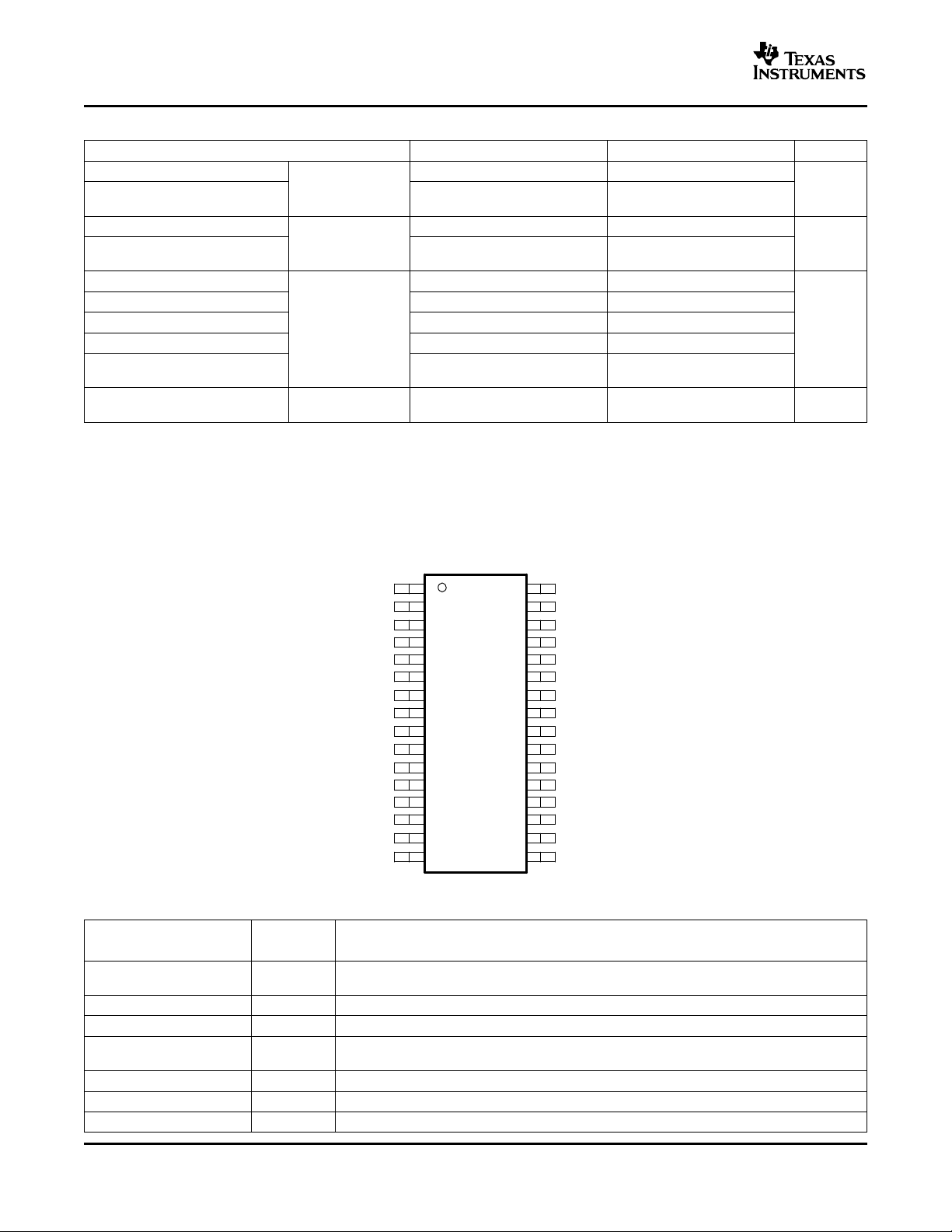
DAP PACKAGE
(TOP VIEW)
Terminal Functions

www.ti.com
VCC
INPUT
GND
400
SOUT
GND
10
Terminal Functions (continued)
TERMINAL
NAME NO.
OUT3 11 O Constant current output
OUT4 12 O Constant current output
OUT5 13 O Constant current output
OUT6 15 O Constant current output
OUT7 16 O Constant current output
OUT8 17 O Constant current output
OUT9 18 O Constant current output
OUT10 20 O Constant current output
OUT11 21 O Constant current output
OUT12 22 O Constant current output
OUT13 23 O Constant current output
OUT14 25 O Constant current output
OUT15 26 O Constant current output
PGND Power ground
SCLK 4 I
SIN 5 I Data input of serial I/F
SOUT 28 O Data output of serial I/F
VCC 32 Power supply voltage
NC 29 – Not Connected
XLAT 3 I
6, 9, 14,,,
19, 24, 27
I/O DESCRIPTION
Data shift clock. Note that the internal connections are switched by MODE (pin #30). At
SCLK↑, the shift-registers selected by MODE shift the data.
Data latch. Note that the internal connections are switched by MODE (pin #30). At XLAT↑, the
latches selected by MODE get new data.
TLC5922
SLVS486A–SEPTEMBER 2003–REVISED MARCH 2005
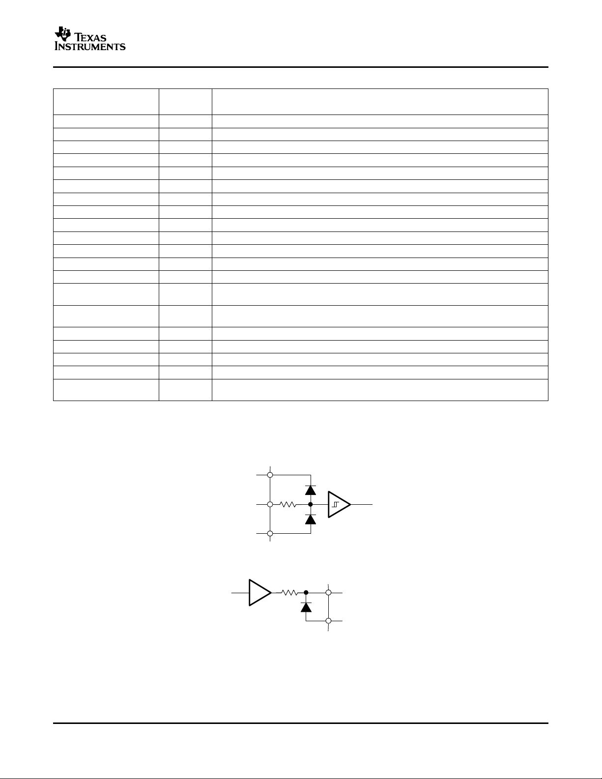
PIN EQUIVALENT INPUT AND OUTPUT SCHEMATIC DIAGRAMS
(Note: Resistor values are equivalent resistance and not tested).
Figure 2. Input Equivalent Circuit (BLANK, XLAT, SCLK, SIN, MODE)
Figure 3. Output Equivalent Circuit
5
 Loading...