TLC5921
LED DRIVER
SLLS390 – SEPTEMBER 1999
1
POST OFFICE BOX 655303 • DALLAS, TEXAS 75265
D
Drive Capability and Output Counts
– 80 mA (Current Sink) x 16 Bits
D
Constant Current Output Range
– 1 to 80 mA (C urrent Value Setting for All
Output Terminals Using External Resistor)
D
Constant Current Accuracy
– ±1% (Typ)
– ±4% (Max) (Maximum Error Between
Bits, All Bits On)
D
Voltage Applied to Constant Current Output
Terminal
– Minimum 0.6 V (Output Current 40 mA)
– Minimum 1 V (Output Current 80 mA)
D
Data Input
– Clock Synchronized 1 Bit Serial Input
D
Data Output
– Clock Synchronized 1 bit Serial Output
(With Timing Selection)
D
Input/Output Signal Level . . . CMOS Level
D
Power Supply V oltage . . . 4.5 V to 5.5V
D
Maximum Output Voltage . . . 17 V (Max)
D
Data Transfer Rate . . . 20 MHz (Max)
D
Operating Free-Air Temperature Range
–20°C to 85°C
D
Available in 32 Pin HTSSOP DAP Package
(PD=3.9 W,
T
A
= 25°C)
D
LOD Function . . . LED Open Detection
(Error Signal Output at LED Disconnection)
D
TSD Function . . . Thermal Shutdown (Turn
Output Off When Junction Temperature
Exceeds Limit)
description
The TLC5921 is a current-sink constant current driver incorporating shift register and data latch. The current
value at constant current output can be set by one external register. The device also incorporates thermal
shutdown (TSD) circuitry which turns constant current output off when the junction temperature exceeds the
limit, and LED open detection (LOD) circuitry to report the LED was disconnected.
Copyright 1999, Texas Instruments Incorporated
PRODUCTION DATA information is current as of publication date.
Products conform to specifications per the terms of Texas Instruments
standard warranty. Production processing does not necessarily include
testing of all parameters.
Please be aware that an important notice concerning availability, standard warranty, and use in critical applications of
Texas Instruments semiconductor products and disclaimers thereto appears at the end of this data sheet.
1
2
3
4
5
6
7
8
9
10
11
12
13
14
15
16
32
31
30
29
28
27
26
25
24
23
22
21
20
19
18
17
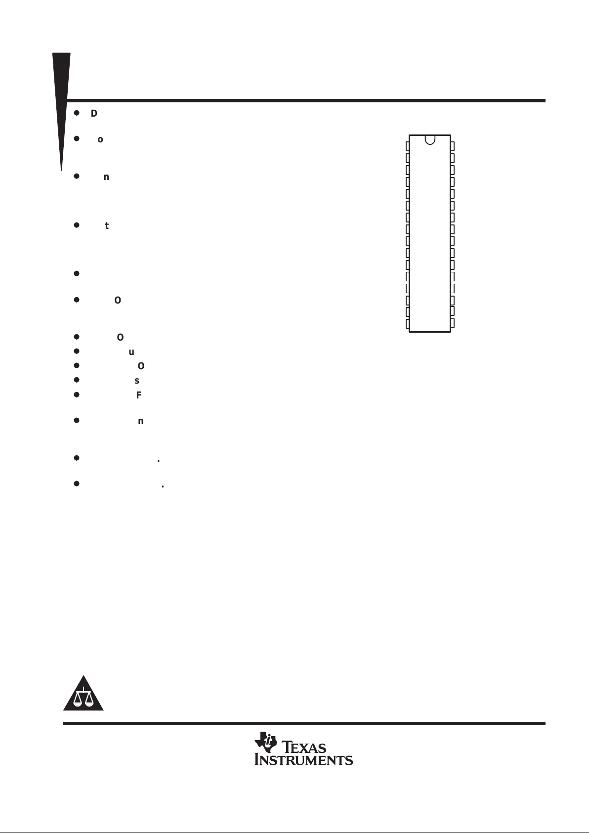
GND
BLANK
XLAT
SCLK
SIN
PGND
OUT0
OUT1
PGND
OUT2
OUT3
OUT4
OUT5
PGND
OUT6
OUT7
VCC
IREF
SOMODE
XDOWN
SOUT
PGND
OUT15
OUT14
PGND
OUT13
OUT12
OUT11
OUT10
PGND
OUT9
OUT8
(TOP VIEW)
DAP PACKAGE
TLC5921
LED DRIVER
SLLS390 – SEPTEMBER 1999
2
POST OFFICE BOX 655303 • DALLAS, TEXAS 75265
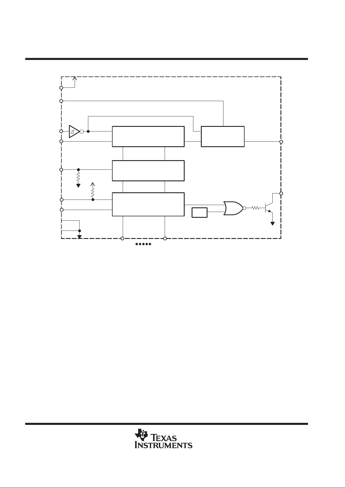
functional block diagram
Timing Selector
16 bits
Data Latch
XLAT
SOUT
OUT0 OUT15
SOMODE
SCLK
SIN
16 bits
Shift Register
16 bits Constant Current Driver
and
LED Disconnection detection
BLANK
IREF
TSD
XDOWN
VCC
GND
PGND
100 kΩ
100 kΩ
TLC5921
LED DRIVER
SLLS390 – SEPTEMBER 1999
3
POST OFFICE BOX 655303 • DALLAS, TEXAS 75265
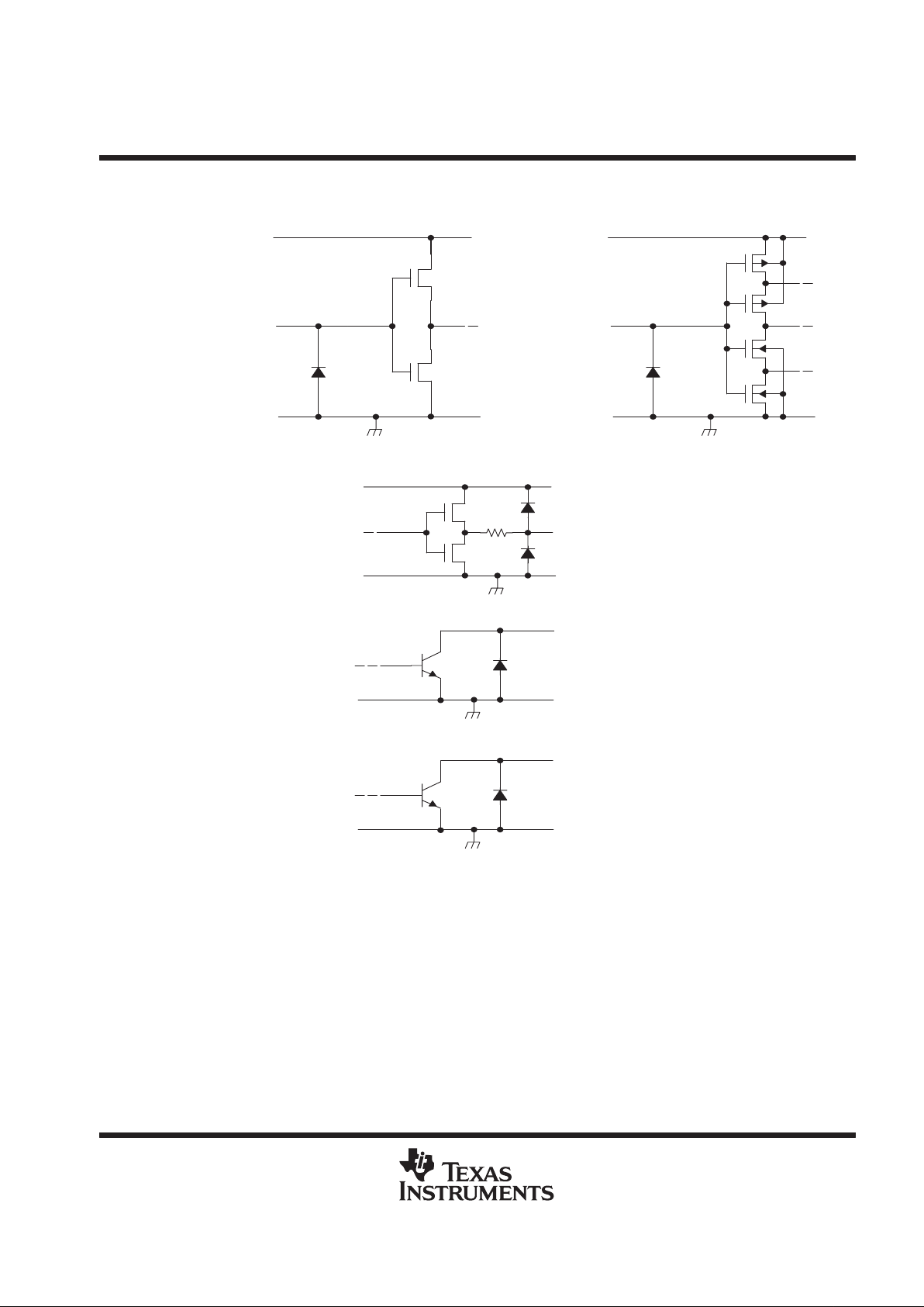
equivalent input and output schematic diagrams
VCC
Input (except SCLK)
INPUT
GND
SOUT
VCC
OUTPUT
GND
XDOWN
GND
XDOWN
OUTn
GND
OUTn
VCC
INPUT
GND
Input (SCLK)
TLC5921
LED DRIVER
SLLS390 – SEPTEMBER 1999
4
POST OFFICE BOX 655303 • DALLAS, TEXAS 75265
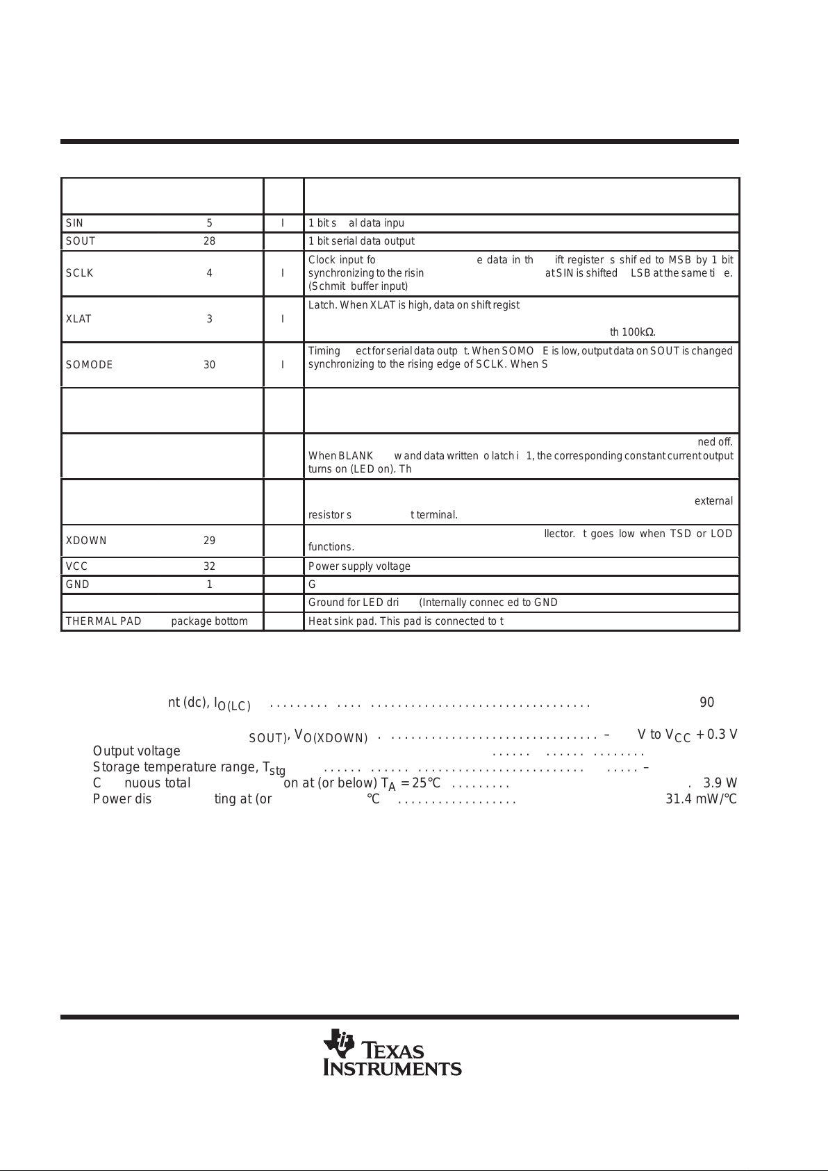
Terminal Functions
TERMINAL
NAME NO.
I/O
DESCRIPTION
SIN
5
I
1 bit serial data input
SOUT
28
O
1 bit serial data output
ÁÁÁÁ
Á
SCLK
ÁÁÁÁ
Á
4
Á
Á
I
ББББББББББББББББББББ
Á
Clock input for data transfer. All the data in the shift register is shifted to MSB by 1 bit
synchronizing to the rising edge of SCLK, and data at SIN is shifted to LSB at the same time.
(Schmitt buffer input)
ÁÁÁÁ
Á
ÁÁÁÁ
Á
XLAT
ÁÁÁÁ
Á
ÁÁÁÁ
Á
3
Á
Á
Á
Á
I
ББББББББББББББББББББ
Á
ББББББББББББББББББББ
Á
Latch. When XLAT is high, data on shift register goes through latch. When XLA T is low, data
is latched. Accordingly, if data on shift register is changed during XLA T high, this new value
is latched (level latch). This terminal is internally pulled down with 100kΩ.
ÁÁÁÁ
Á
SOMODE
ÁÁÁÁ
Á
30
Á
Á
I
ББББББББББББББББББББ
Á
Timing select for serial data output. When SOMODE is low , output data on SOUT is changed
synchronizing to the rising edge of SCLK. When SOMODE is high, output data on SOUT
is changed synchronizing to the falling edge of SCLK.
ÁÁÁÁ
Á
OUT0 – OUT15
ÁÁÁÁ
Á
7,8,10,1 1,12,13,
15,16,17,18,20,
21,22,23,25,26
Á
Á
O
ББББББББББББББББББББ
Á
Constant current output.
ÁÁÁÁ
Á
BLANK
ÁÁÁÁ
Á
2
Á
Á
I
ББББББББББББББББББББ
Á
Blank(Light off). When BLANK is high, all the output of constant current driver is turned off.
When BLANK is low and data written to latch is 1, the corresponding constant current output
turns on (LED on). This terminal is internally pulled up with 100kΩ.
ÁÁÁÁ
Á
IREF
ÁÁÁÁ
Á
31
Á
Á
I
ББББББББББББББББББББ
Á
Constant current value setting. LED current is set to desired value by connecting external
resistor between IREF and GND. The 38 times current compared to current across external
resistor sink on output terminal.
ÁÁÁÁ
Á
XDOWN
ÁÁÁÁ
Á
29
Á
Á
O
ББББББББББББББББББББ
Á
Error output. XDOWN is configured as open collector. It goes low when TSD or LOD
functions.
VCC
32
Power supply voltage
GND
1
Ground
PGND
6,9,14,19,24,27
Ground for LED driver. (Internally connected to GND)
THERMAL PAD
package bottom
Heat sink pad. This pad is connected to the lowest potential to IC or thermal layer.
absolute maximum ratings (see Note 1)
†
Supply voltage, VCC – 0.3 V to 7 V. . . . . . . . . . . . . . . . . . . . . . . . . . . . . . . . . . . . . . . . . . . . . . . . . . . . . . . . . . . . . . .
Output current (dc), I
O(LC)
90 mA. . . . . . . . . . . . . . . . . . . . . . . . . . . . . . . . . . . . . . . . . . . . . . . . . . . . . . . . . . . . . . . .
Input voltage range, VI – 0.3 V to V
CC
+ 0.3 V. . . . . . . . . . . . . . . . . . . . . . . . . . . . . . . . . . . . . . . . . . . . . . . . . . . . . .
Output voltage range, V
O(SOUT)
, V
O(XDOWN)
– 0.3 V to V
CC
+ 0.3 V. . . . . . . . . . . . . . . . . . . . . . . . . . . . . . . . .
Output voltage range, V
O(OUTn)
– 0.3 V to 18 V. . . . . . . . . . . . . . . . . . . . . . . . . . . . . . . . . . . . . . . . . . . . . . . . . . . .
Storage temperature range, T
stg
–40°C to 150°C. . . . . . . . . . . . . . . . . . . . . . . . . . . . . . . . . . . . . . . . . . . . . . . . . . .
Continuous total power dissipation at (or below) TA = 25°C 3.9 W. . . . . . . . . . . . . . . . . . . . . . . . . . . . . . . . . . . .
Power dissipation rating at (or above) TA = 25°C 31.4 mW/°C. . . . . . . . . . . . . . . . . . . . . . . . . . . . . . . . . . . . . . .
†
Stresses beyond those listed under “absolute maximum ratings” may cause permanent damage to the device. These are stress ratings only, and
functional operation of the device at these or any other conditions beyond those indicated under “recommended operating conditions” is not
implied. Exposure to absolute-maximum-rated conditions for extended periods may affect device reliability.
NOTE 1: All voltage values are with respect to GND terminal.
TLC5921
LED DRIVER
SLLS390 – SEPTEMBER 1999
5
POST OFFICE BOX 655303 • DALLAS, TEXAS 75265
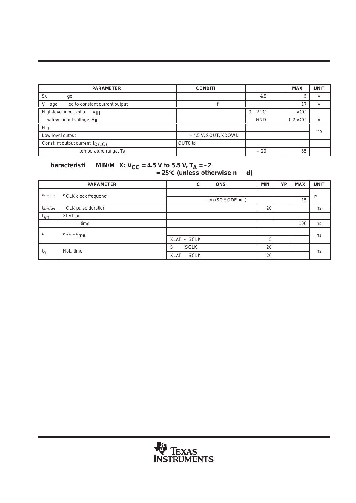
recommended operating conditions
dc characteristics
PARAMETER
CONDITIONS
MIN
NOM
MAX
UNIT
Supply voltage, V
CC
4.5
5
ÁÁÁ
5.5
V
Voltage applied to constant current output, V
O
OUT0 to OUT15 off
ÁÁÁ
17
V
High-level input voltage, V
IH
0.8 VCC
ÁÁÁ
VCC
V
Low-level input voltage, V
IL
GND
ÁÁÁ
0.2 VCC
V
High-level output current, I
OH
VCC = 4.5 V, SOUT
ÁÁÁ
–1
Low-level output current, I
OL
VCC = 4.5 V, SOUT, XDOWN
ÁÁÁ
1
mA
Constant output current, I
O(LC)
OUT0 to OUT15
ÁÁÁ
80
mA
Operating free-air temperature range, T
A
–20
ÁÁÁ
85
°C
ac characteristics, MIN/MAX: V
CC
= 4.5 V to 5.5 V, TA = –20 to 85°C
TYP: V
CC
= 5 V, TA = 25°C (unless otherwise noted)
PARAMETER
CONDITIONS
MIN
TYP
MAX
UNIT
At single operation
20
f
SCLK
SCLK clock frequenc
y
At cascade operation (SOMODE = L)
15
MH
z
twh/twlSCLK pulse duration
20
ns
t
wh
XLAT pulse duration
10
ns
tr/t
f
Rise/fall time
100
ns
p
SIN – SCLK
5
tsuSetup time
XLAT – SCLK
5
ns
SIN – SCLK
20
thHold time
XLAT – SCLK
20
ns
 Loading...