Texas Instruments TLC5920DLR, TLC5920DL Datasheet

TLC5920
16x8 BIT LED DRIVER/CONTROLLER
SLAS264 – MARCH 2000
1
POST OFFICE BOX 655303 • DALLAS, TEXAS 75265
D
Drive Capability:
– Segment . . . 30 mA × 16 Bits
– Common . . . 640 mA
D
Constant Current Output ...3 mA to 30 mA
(Current Value Setting for All Channels
Using External Resistor)
D
Constant Current Accuracy ±6% (Maximum
Error Between Bits)
D
Data Input: Clock Synchronized Serial Input
D
LED Type Applied Cathode Common
D
Logic Power Supply Voltage 4.5 V to 5.5 V
D
LED Power Supply Voltage 4.5 V to 5.5 V
D
Operating Frequency . . . 10 MHz
D
Operating Free-Air Temperature Range
–20°C to 85°C
D
48-Pin SSOL Package
description
The TLC5920 is an LED driver incorporating a
16-channel shift register, data latch, and constant
current circuitry with current value control and
8-channel common driver into a single chip. The
constant output current is capable of 30 mA for 16
bits simultaneously , and the current value can be
set by one external register. This device also
includes a 16-bit segment driver and 8-bit
common driver; therefore, the monocolor LED
array with 16 × 8 dots can be driven by only one
TLC5920, and a two-color LED array with 16 x 16
dots can be driven by two TLC5920s.
Copyright 2000, Texas Instruments Incorporated
PRODUCTION DATA information is current as of publication date.
Products conform to specifications per the terms of Texas Instruments
standard warranty. Production processing does not necessarily include
testing of all parameters.
Please be aware that an important notice concerning availability, standard warranty, and use in critical applications of
Texas Instruments semiconductor products and disclaimers thereto appears at the end of this data sheet.
1
2
3
4
5
6
7
8
9
10
11
12
13
14
15
16
17
18
19
20
21
22
23
24
48
47
46
45
44
43
42
41
40
39
38
37
36
35
34
33
32
31
30
29
28
27
26
25
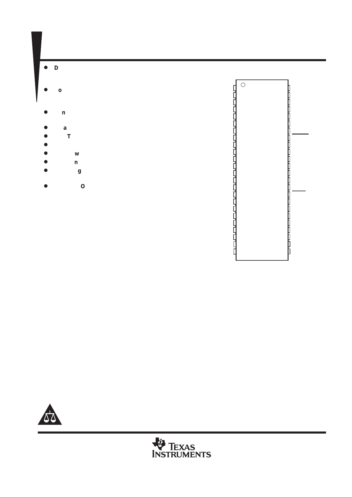
COM3
COM2
COM1
COM0
GNDLED
NC
NC
VLED
S0
S1
S2
S3
S4
S5
S6
S7
IREF
VLED
VANA
NC
GNDANA
S8
S9
S10
GNDLED
COM4
COM5
COM6
COM7
GNDLED
SIN
LATCH
SCLK
BLANK
CSEL0
GNDLOG
CSEL1
CSEL2
VLOG
DSEL
SOUT
VLED
DSEL
S15
S14
S13
S12
S11
DL PACKAGE
(TOP VIEW)

TLC5920
16x8 BIT LED DRIVER/CONTROLLER
SLAS264 – MARCH 2000
2
POST OFFICE BOX 655303 • DALLAS, TEXAS 75265
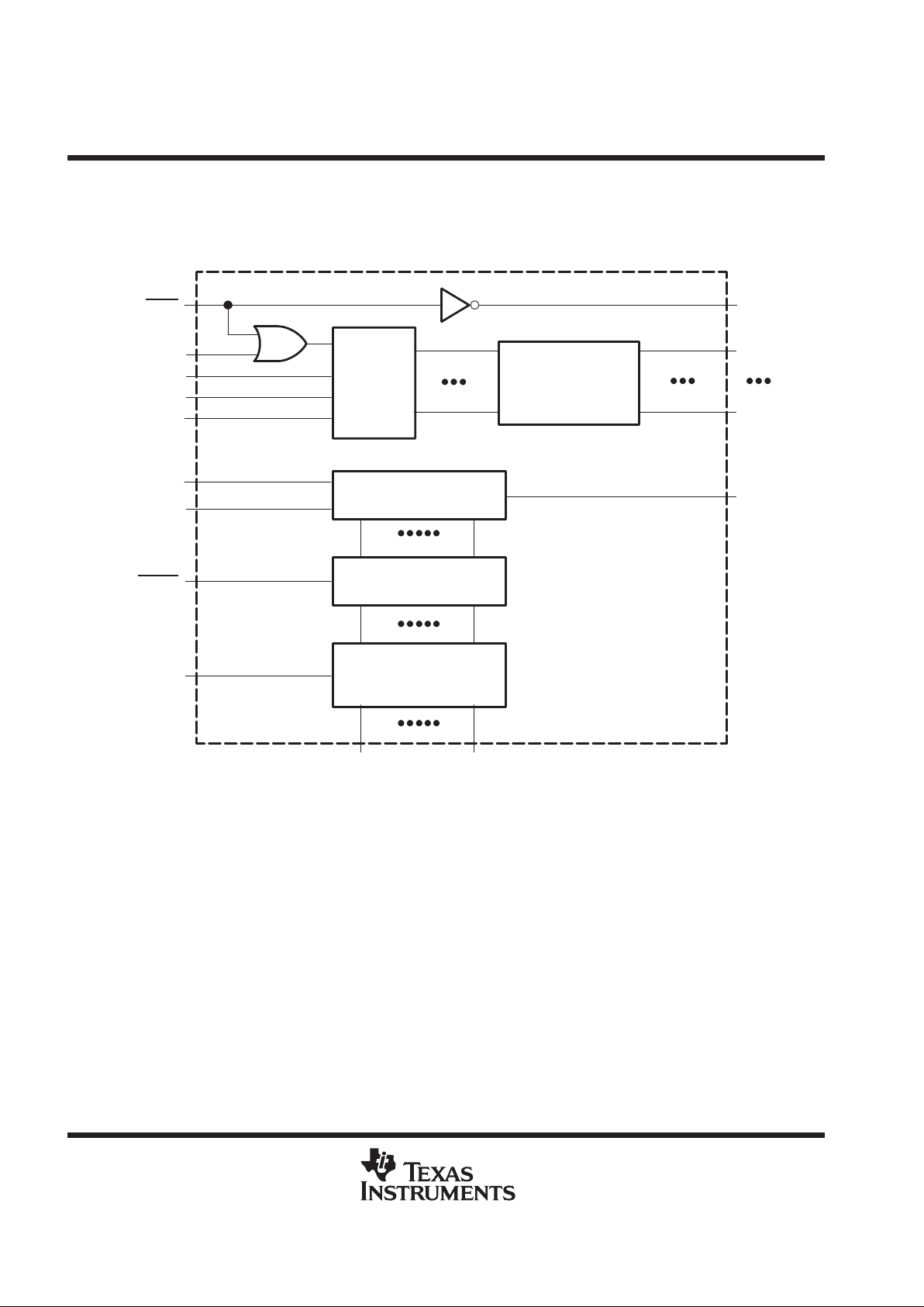
functional block diagram
S15
Common
Driver
3 TO 8
Decoder
S0
16 bits
Shift Register
16 bits
Data Latch
Segment Driver
and
Current Control
DSEL
BLANK
CSEL0
CSEL1
CSEL2
SIN
SCLK
LATCH
IREF
DSEL
COM0
COM7
SOUT

TLC5920
16x8 BIT LED DRIVER/CONTROLLER
SLAS264 – MARCH 2000
3
POST OFFICE BOX 655303 • DALLAS, TEXAS 75265
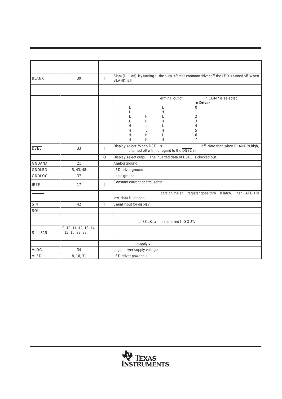
Terminal Functions
TERMINAL
NAME NO.
I/O
DESCRIPTION
ÁÁÁ
Á
BLANK
ÁÁÁÁ
Á
39
Á
Á
I
ББББББББББББББББББББ
Á
Blank(light off). By turning all the output for the common driver off, the LED is turned off. When
BLANK is high, the LED is turned off.
ÁÁÁ
Á
COM0 – COM7
ÁÁÁÁ
Á
4, 3, 2, 1, 47, 46,
45, 44
Á
Á
O
ББББББББББББББББББББ
Á
LED common driver output
ÁÁÁ
Á
ÁÁÁ
Á
ÁÁÁ
Á
ÁÁÁ
Á
ÁÁÁ
Á
CSEL0 – 2
ÁÁÁÁ
Á
ÁÁÁÁ
Á
ÁÁÁÁ
Á
ÁÁÁÁ
Á
ÁÁÁÁ
Á
38, 36, 35
Á
Á
Á
Á
Á
Á
Á
Á
Á
Á
I
ББББББББББББББББББББ
Á
ББББББББББББББББББББ
Á
ББББББББББББББББББББ
Á
ББББББББББББББББББББ
Á
ББББББББББББББББББББ
Á
Common driver select. One terminal out of COM0 through COM7 is selected.
2 1 0 Common Driver
LLL 0
LLH 1
LHL 2
LHH 3
HLL 4
HLH 5
HHL 6
HHH 7
ÁÁÁ
Á
DSEL
ÁÁÁÁ
Á
33
Á
Á
I
ББББББББББББББББББББ
Á
Display select. When DSEL is high, the LED is turned off. Note that, when BLANK is high,
the LED is turned off with no regard to the DSEL
input.
DSEL
30
O
Display select output. The inverted data of DSEL is clocked out.
GNDANA
21
Analog ground
GNDLED
5, 43, 48
LED driver ground
GNDLOG
37
Logic ground
ÁÁÁ
Á
IREF
ÁÁÁÁ
Á
17
Á
Á
I
ББББББББББББББББББББ
Á
Constant current control setting. The LED current is set to the desired value by connecting
an external resistor between IREF and GND.
ÁÁÁ
Á
LATCH
ÁÁÁÁ
Á
41
Á
Á
I
ББББББББББББББББББББ
Á
Latch. When LATCH is high, data on the shift register goes through latch. When LATCH is
low, data is latched.
SIN
42
I
Serial input for display
SOUT
32
O
Serial output for display
ÁÁÁ
Á
SCLK
ÁÁÁÁ
Á
40
Á
Á
I
ББББББББББББББББББББ
Á
Synchronous clock input for serial data transfer. The input data of SIN is synchronized to
the rising edge of SCLK, and transferred to SOUT.
ÁÁÁ
Á
S0 – S15
ÁÁÁÁ
Á
9, 10, 11, 12, 13, 14,
15, 16, 22, 23, 24,
25, 26, 27, 28, 29
Á
Á
O
ББББББББББББББББББББ
Á
LED segment driver output
VANA
19
Analog power supply voltage
VLOG
34
Logic power supply voltage
VLED
8, 18, 31
LED driver power supply voltage

TLC5920
16x8 BIT LED DRIVER/CONTROLLER
SLAS264 – MARCH 2000
4
POST OFFICE BOX 655303 • DALLAS, TEXAS 75265
absolute maximum ratings† (see Note 1)
Logic supply voltage, V
(LOG)
– 0.3 V to 7 V. . . . . . . . . . . . . . . . . . . . . . . . . . . . . . . . . . . . . . . . . . . . . . . . . . . . . . . .
LED supply voltage, V
(LED)
– 0.3 V to 7 V. . . . . . . . . . . . . . . . . . . . . . . . . . . . . . . . . . . . . . . . . . . . . . . . . . . . . . . . .
Analog supply voltage, V
(ANA)
– 0.3 V to 7 V. . . . . . . . . . . . . . . . . . . . . . . . . . . . . . . . . . . . . . . . . . . . . . . . . . . . . . .
Output current, I
OH(S)
– 32 mA. . . . . . . . . . . . . . . . . . . . . . . . . . . . . . . . . . . . . . . . . . . . . . . . . . . . . . . . . . . . . . . . . .
Output current, I
OL(C)
650 mA. . . . . . . . . . . . . . . . . . . . . . . . . . . . . . . . . . . . . . . . . . . . . . . . . . . . . . . . . . . . . . . . . . .
Input voltage range, VI – 0.3 V to V
(LOG)
+ 0.3 V. . . . . . . . . . . . . . . . . . . . . . . . . . . . . . . . . . . . . . . . . . . . . . . . . . . .
Output voltage range, VO – 0.3 V to V
(LOG)
+ 0.3 V. . . . . . . . . . . . . . . . . . . . . . . . . . . . . . . . . . . . . . . . . . . . . . . . .
Continuous total power dissipation 1500 mW. . . . . . . . . . . . . . . . . . . . . . . . . . . . . . . . . . . . . . . . . . . . . . . . . . . . . .
Thermal resistance 83°C/W. . . . . . . . . . . . . . . . . . . . . . . . . . . . . . . . . . . . . . . . . . . . . . . . . . . . . . . . . . . . . . . . . . . . . .
Operating free-air temperature range (see Note 2), T
A
– 20 to 85°C. . . . . . . . . . . . . . . . . . . . . . . . . . . . . . . . . . .
Storage temperature range, T
stg
–40°C to 125°C. . . . . . . . . . . . . . . . . . . . . . . . . . . . . . . . . . . . . . . . . . . . . . . . . . .
†
Stresses beyond those listed under “absolute maximum ratings” may cause permanent damage to the device. These are stress ratings only, and
functional operation of the device at these or any other conditions beyond those indicated under “recommended operating conditions” is not
implied. Exposure to absolute-maximum-rated conditions for extended periods may affect device reliability.
NOTES: 1. All voltage values are with respect to GND terminal.
2. TJ ≤ 150°C (refer to appendix thermal condition).
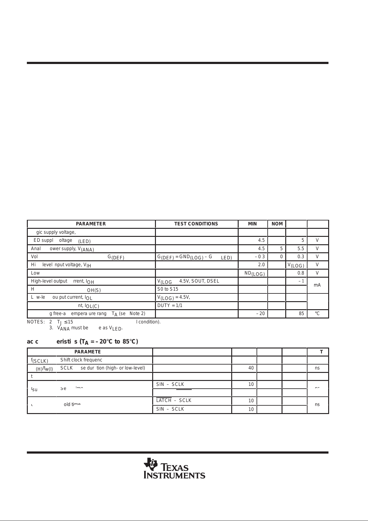
recommended operating conditions
dc characteristics (see Note 3)
PARAMETER
TEST CONDITIONS
MIN
NOM
MAX
UNIT
Logic supply voltage, V
(LOG)
4.5
5
5.5
V
LED supply voltage, V
(LED)
4.5
5
5.5
V
Analog power supply, V
(ANA)
4.5
5
5.5
V
Voltage between GND and V
(DEF), G(DEF)
G
(DEF)
= GND
(LOG)
– GND
(LED)
–0.3
0
0.3
V
High-level input voltage, V
IH
2.0
V
(LOG)
V
Low-level input voltage, V
IL
GND
(LOG)
0.8
V
High-level output current, I
OH
V
(LOG)
= 4.5V, SOUT, DSEL
–1
High-level output current, I
OH(S)
S0 to S15
–30
mA
Low-level output current, I
OL
V
(LOG)
= 4.5V, SOUT, DSEL
1.6
Low-level output current, I
OL(C)
DUTY = 1/16, COM0 to COM7
640
mA
Operating free-air temperature range, TA (see Note 2)
–20
85
°C
NOTES: 2 TJ ≤ 150°C (refer to appendix thermal condition).
3. V
ANA
must be same as V
LED
.
ac characteristics (TA = –20°C to 85°C)
PARAMETER
TEST CONDITIONS
MIN
NOM
MAX
UNIT
f
(SCLK)
Shift clock frequency
10
MHz
t
w(H)/tw(l)
SCLK pulse duration (high- or low-level)
40
ns
tr/t
f
Rise/fall time
100
ns
p
SIN – SCLK
10
tsuSetup time
SCLK – LATCH
10
ns
LATCH – SCLK
10
thHold time
SIN – SCLK
10
ns
 Loading...