D
Drive Capability and Output Counts
– 80 mA (Current Sink) x 16 Bits
D
Constant Current Output Range
– 5 to 80 mA (Current Value Setting for All
Output Terminals Using External Resistor
and Internal Brightness Control Register)
D
Constant Current Accuracy
– ±4 % (Maximum Error Between Bits)
D
Voltage Applied to Constant Current Output
Terminals
– Minimum 0.4 V (Output Current 5 mA to
40 mA)
– Minimum 0.7 V (Output Current 40 mA to
80 mA)
D
1024 Gray Scale Display
– Pulse Width Control 1024 Steps
D
Brightness Adjustment
– All Output Current Adjustment for 64
Steps (Adjustment for Brightness
Deviation Between LED Modules)
– Output Current Adjustment by Output
(OUT0 to OUT15) for 128 Steps
(Adjustment for Brightness Deviation
Between Dots)
– Brightness Control by 16 Steps
Frequency Division Gray Scale Control
Clock (Brightness Adjustment for Panel)
D
Gray Scale Clock Generation
– Gray Scale Control Clock Generation by
Internal PLL or External Input Selectable
D
Clock Invert/Noninvert Selectable at
Cascade Operation
– Clock Invert Selectable to Reduce
Changes in Duty Ratio
†
Adjustable for these functions independently.
‡
Allows to write all the data at port A by setting.
†
LED DRIVER
SLLS402 – DECEMBER 1999
D
Protection
– Watchdog Timer (WDT) Function (Turn
Output Off When Scan Signal Stopped)
– Thermal Shutdown (TSD) Function (Turn
Output Off When Junction Temperature
Exceeds Limit)
D
LOD
– LED Open Detection (Detection for LED
Disconnection)
D
Data Input/Output
– Port A (for Data Display)
– Clock Synchronized 10 Bit Parallel Input
(Schmitt-Triggered Input)
– Clock Synchronized 10 Bit Parallel
Output (3-State Output)
– Port B (for Dot Correction Data)
– Clock Synchronized 7 Bit Parallel Input
(Schmitt-Triggered Input)
– Clock Synchronized 7 Bit Parallel Output
D
Input/Output Signal Level
– CMOS Level
D
Power Supply Voltage
– 4.5 V to 5.5 V (Logic, Analog and
Constant Current)
– 3 V to 5.5 V (Interface)
D
Maximum Output Voltage . . . 15 V
D
Data Transfer Rate . . . 20 MHz (Max)
D
Gray Scale Clock Frequency
– 16 MHz (Max) Using Internal PLL
– 8 MHz (Max) Using External Clock
D
Operating Free-Temperature Range
–20°C to 85°C
D
100-Pin Package HTQFP (P
T
= 25°C)
A
‡
= 4.7 W,
D
TLC5911
Please be aware that an important notice concerning availability, standard warranty, and use in critical applications of
Texas Instruments semiconductor products and disclaimers thereto appears at the end of this data sheet.
PRODUCTION DATA information is current as of publication date.
Products conform to specifications per the terms of Texas Instruments
standard warranty. Production processing does not necessarily include
testing of all parameters.
POST OFFICE BOX 655303 • DALLAS, TEXAS 75265
Copyright 1999, Texas Instruments Incorporated
1

TLC5911
LED DRIVER
SLLS402 – DECEMBER 1999
description
The TLC591 1 is a constant current driver incorporating shift register, data latch, and constant current circuitry
with a current value adjustable, PLL circuitry for gray scale control clock generation, and 1024 gray scale display
using pulse width control. The output current is maximum 80 mA with 16 bits, and the current value of constant
current output can be set by one external resistor. The device has two channel I/O ports. The brightness
deviation between LED modules (ICs) can be adjusted by external data input from the display data port, and
the brightness control for the panel can be accomplished by the brightness adjustment circuitry . Independent
of these functions, the device incorporates the shift register and data latch to correct the deviation between
LEDs by adjusting the output current using data from the dot correction data port. Moreover, the device
incorporates WDT circuitry, which turns constant current output off when the scan signal stops during the
dynamic scanning operation, and TSD circuitry, which turns constant current output off when the junction
temperature exceeds the limit. Also the LED open detection (LOD) circuitry is used to make error signal output
at the LED disconnection.
pin assignments
PZP PACKAGE
(TOP VIEW)
GNDLED
OUT0
OUT1
GNDLED
OUT2
OUT3
GNDLED
OUT4
OUT5
GNDLED
OUT6
OUT7
GNDLED
OUT8
OUT9
GNDLED
OUT10
OUT11
GNDLED
OUT12
OUT13
GNDLED
OUT14
OUT15
GNDLED
1
2
3
4
5
6
7
8
9
10
11
12
13
14
15
16
17
18
19
20
21
22
23
24
25
TEST3
TEST2
99
100
27
26
GNDLOG
TEST1
DPOL
DCENA
95
96
97
98
31
30
29
28
BCENA
VCCLOG
DCDIN6
92
93
94
34
33
32
DCDIN5
DCDIN4
DCDIN3
89
90
91
37
36
35
DCDIN2
DCDIN1
DCDIN0
86
87
88
40
38
39
DIN9
DIN8
84
85
42
41
DIN7
DIN6
82
83
44
43
DIN5
DIN4
80
81
46
45
DIN3
DIN2
78
79
48
47
DIN1
DIN0
76
77
50
49
75
74
73
72
71
70
69
68
67
66
65
64
63
62
61
60
59
58
57
56
55
54
53
52
51
VCOIN
RBIAS
MAG0
MAG1
MAG2
PDOUT
GSPOL
GSCLK
BLANK
XENABLE
XOE
DCLK
XLA TCH
DCCLK
XDCLAT
RSEL0
RSEL1
LEDCHK
NC
WDTRG
XDOWN1
XDOWN2
BOUT
XGSOUT
XPOUT
IREF
TSENA
VCCLED
XDWN2TST
2
WDCAP
XDPOUT
GNDANA
POST OFFICE BOX 655303 • DALLAS, TEXAS 75265
VCCANA
DCDOUT0
DCDOUT1
DCDOUT2
DCDOUT3
DCDOUT4
DOUT0
DOUT1
DCDOUT5
DCDOUT6
DOUT2
DOUT3
DOUT4
DOUT5
DOUT6
DOUT7
DOUT8
DOUT9
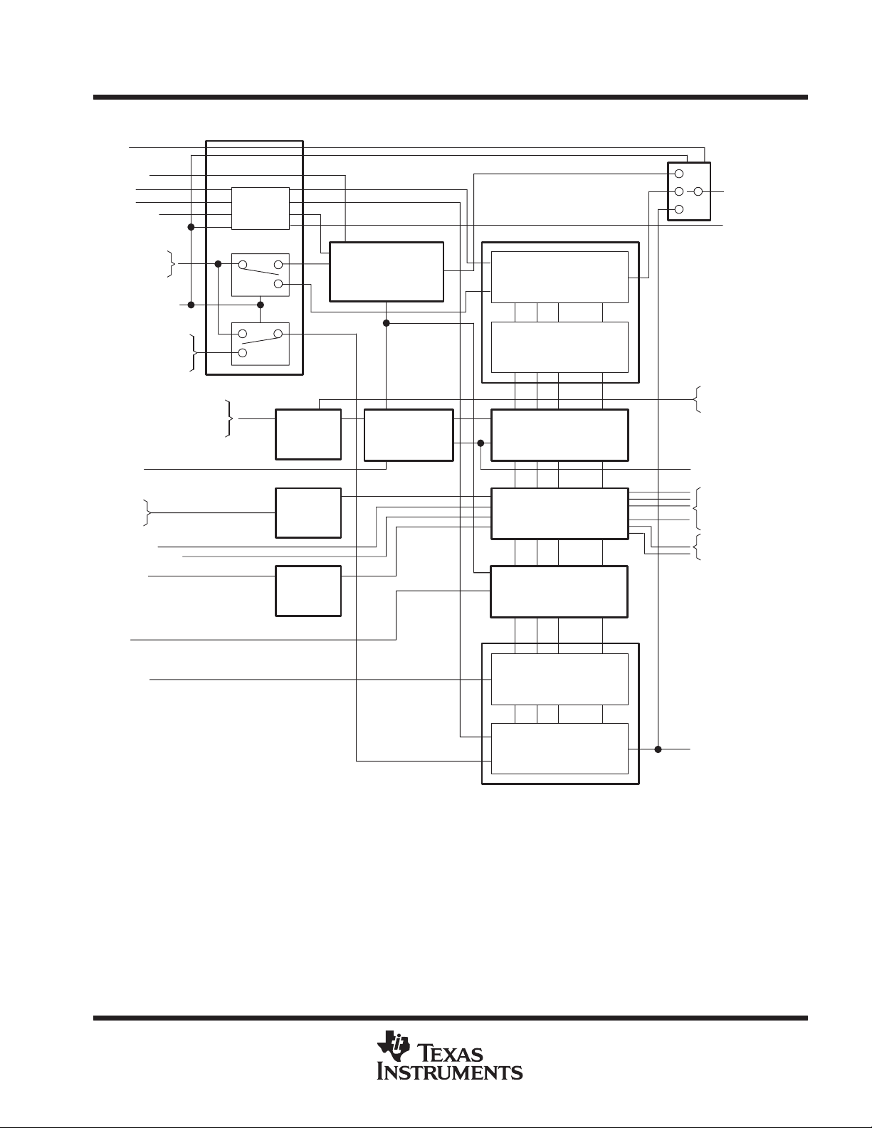
functional block diagram
XOE
BCENA
DCLK
DPOL
XENABLE
DCLK
Control
TLC5911
LED DRIVER
SLLS402 – DECEMBER 1999
DOUT(9–0)
XDPOUT
DIN(9–0),
XLATCH
RSEL(1–0)
DCDIN(6–0),
XDCLAT,
DCCLK
MAG(2–0), GSPOL,
GSCLK, RBIAS,
VCOIN, PDOUT
BLANK
WDCAP
WDTRG
LEDCHK
XDOWN2TST
TSENA
IREF
DCENA
1 x 10 bit B.C.
Data Shift Register
Data Latch
8
PLL
WDT
TSD
10 bit
Clock Countor
16 x 10 bit
Data Shift Register
..........
16 x 10 bit
Data Latch
..........
16 x 10 bit
Data Comparator
..........
16 bit
LED Driver+LOD
..........
16 bit
Current Controller
..........
16 x 7 bit
D.C. Data Latch
XPOUT
XGSOUT
BOUT
OUT0
· · ·
OUT15
XDOWN1
XDOWN2
..........
16 x 7 bit
D.C. Data Shift Register
Legend:
B.C. (Brightness Control): Adjustment for brightness deviation between LED modules, and between panels.
D.C. (Dot Control): Adjustment for brightness deviation between dots.
NOTE: All the input terminals are with Schmitt triggered inverter except RBIAS, VCOIN, PDOUT, IREF and WDCAP.
POST OFFICE BOX 655303 • DALLAS, TEXAS 75265
DCDOUT(6–0)
3
TLC5911
CONNECTION
LED DRIVER
SLLS402 – DECEMBER 1999
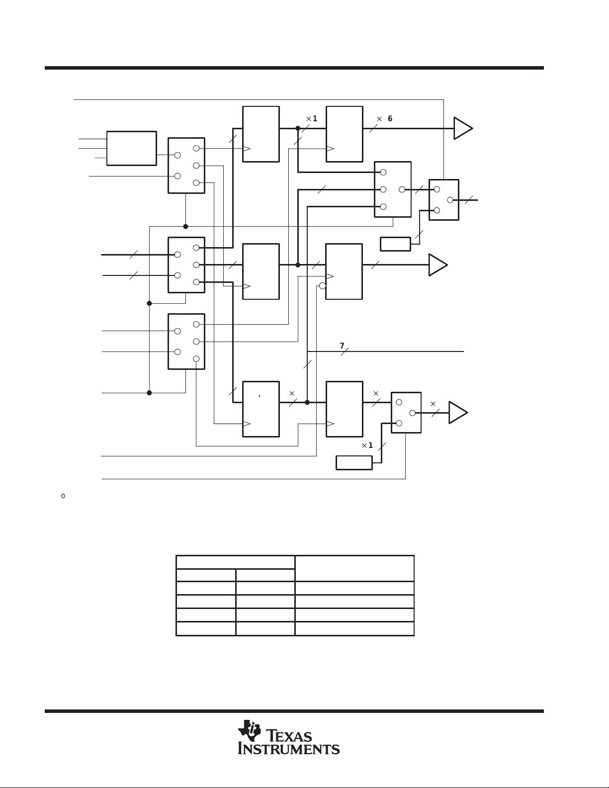
functional block diagram for shift register and data latch
XOE
DCLK
DPOL
XENABLE
DCCLK
DIN(9–0)
DCDIN(6–0)
XLATCH
XDCLAT
RSEL(1–0)
DCLK
Controller
10
7
DATA
10
a
A
b
B
c
a
A
b
B
c
a
A
b
B
c
S/R
B.C.
S/R
7
D.C.
S/R
10 16 10 16
†
‡
7 16
DATA
LATCH
10 10
10 1010
B.C.
LATCH
7
D.C.
LATCH
7 16
a
b
c
HI–Z
DATA
Comparator
A
H
L
L
H
10
Clock Counter
Current Controller
7 16
10
DOUT(9–0)
DCDOUT(6–0)
DATA
Comparator
7 16
BCENA
DCENA
†
Connecting to 16th 10-bit Bus
‡
Connecting to 16th 7-bit Bus
Legend:
B.C. (Brightness Control): Adjustment for brightness deviation between LED modules, and between panels.
D.C. (Dot Control): Adjustment for brightness deviation between dots.
RSEL
RSEL1 RSEL0
L L A – a, B – c
L H A – b, B – c
H L A – c
H H INHIBIT
Default
4
POST OFFICE BOX 655303 • DALLAS, TEXAS 75265
I/O
DESCRIPTION
Á
Á
Á
Á
ÁÁ
ÁÁ
ÁÁ
Á
Á
Á
Á
Á
Á
Á
Á
ÁÁ
ÁÁ
ÁÁ
ÁÁ
Á
Á
Á
ÁÁ
Á
Á
ÁÁ
ÁÁ
Á
ÁÁ
Á
Á
ÁÁ
ÁÁ
Á
Á
Á
ÁÁ
ÁÁ
Á
Á
Á
ÁÁ
ÁÁ
Á
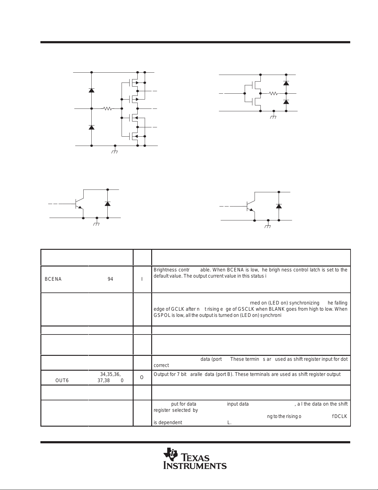
equivalent input and output schematic diagrams
TLC5911
LED DRIVER
SLLS402 – DECEMBER 1999
Input
VCCIF
INPUT
GNDLOG
XDOWN1, XDOWN2
XDOWN1, XDOWN2
GNDLOG
Terminal Functions
DOUT0–9, DCDOUT0–6, XGSOUT, XPOUT, BOUT
VCCLOG
OUTPUT
GNDLOG
OUTn
OUTn
GNDLED
TERMINAL
NAME NO.
ÁÁÁÁ
BCENA
ÁÁÁÁ
ÁÁÁÁ
BLANK
ÁÁÁÁ
ÁÁÁÁ
BOUT
DCCLK
ÁÁÁÁ
DCDIN0 –
DCDIN6
DCDOUT0 –
ÁÁÁÁ
DCDOUT6
DCENA
ÁÁÁÁ
DCLK
ÁÁÁÁ
ÁÁÁÁ
94
ÁÁÁÁ
ÁÁÁÁ
67
ÁÁÁÁ
ÁÁÁÁ
53
62
ÁÁÁÁ
86,87,88,
89,90,91,92
34,35,36,
ÁÁÁÁ
37,38,39,40
95
ÁÁÁÁ
64
ÁÁÁÁ
Brightness control enable. When BCENA is low, the brightness control latch is set to the
ББББББББББББББББББББ
default value. The output current value in this status is 100% of the value set by an external
I
resistor. The frequency division ratio of GSCLK is1/1. When BCENA is high, writing to
ББББББББББББББББББББ
brightness control latch is enabled.
Blank (Light off). When BLANK is high, all output of the constant current driver are turned
ББББББББББББББББББББ
off. When GSPOL is high, all the output is turned on (LED on) synchronizing to the falling
edge of GCLK after next rising edge of GSCLK when BLANK goes from high to low. When
I
ББББББББББББББББББББ
GSPOL is low, all the output is turned on (LED on) synchronizing to the rising edge of GCLK
ББББББББББББББББББББ
after next falling edge of GSCLK when BLANK goes from high to low.
O
BLANK buffered output
Clock input for data transfer. The input data is from DCDIN (port B) . The output data at
DCDOUT . All data on the shift register for dot correction data from DCDIN is shifted by 1 bit
I
ББББББББББББББББББББ
and is synchronized to the rising edge of DCCLK.
Input for 7 bit parallel data (port B). These terminals are used as shift register input for dot
I
correction data.
Output for 7 bit parallel data (port B). These terminals are used as shift register output for
O
ББББББББББББББББББББ
dot correction data.
Latch enable for dot correction data. When DCENA is low, the latch is set to the default value.
I
At this time, the output current value is 100% of the value set by an external resistor.
ББББББББББББББББББББ
Clock input for data transfer. The input data is from DIN (port A) , all the data on the shift
register selected by RSEL0, 1 and the output data at DOUT are shifted by 1 bit and
I
ББББББББББББББББББББ
synchronized to DCLK. Note that whether synchronizing to the rising or falling edge of DCLK
is dependent on the value of DPOL.
POST OFFICE BOX 655303 • DALLAS, TEXAS 75265
5
TLC5911
I/O
DESCRIPTION
Á
Á
Á
Á
Á
Á
Á
Á
Á
Á
Á
Á
Á
Á
Á
Á
Á
Á
Á
Á
Á
Á
Á
Á
Á
Á
Á
Á
Á
Á
Á
Á
Á
Á
Á
Á
Á
Á
Á
Á
Á
Á
Á
Á
Á
Á
Á
Á
Á
Á
Á
Á
Á
Á
Á
Á
Á
Á
Á
LED DRIVER
SLLS402 – DECEMBER 1999
TERMINAL
NAME NO.
ÁÁÁÁ
DIN0 – DIN9
ÁÁÁÁ
DOUT0 – DOUT9
ÁÁÁÁ
DPOL
GNDANA
GNDLOG
GNDLED
ÁÁÁÁ
GSCLK
ÁÁÁÁ
ÁÁÁÁ
GSPOL
IREF
ÁÁÁÁ
ÁÁÁÁ
LEDCHK
ÁÁÁÁ
MAG0 – MAG2
NC
OUT0 – DOUT15
ÁÁÁÁ
PDOUT
RBIAS
ÁÁÁÁ
RSEL0
ÁÁÁÁ
RSEL1
ÁÁÁÁ
ÁÁÁÁ
TEST1 – TEST3
THERMAL PAD
TSENA
VCCANA
VCCLOG
VCCLED
VCOIN
WDCAP
ÁÁÁÁ
ÁÁÁÁ
ÁÁÁÁ
ÁÁÁÁ
ÁÁÁÁ
ÁÁÁÁ
ÁÁÁÁ
ÁÁÁÁ
ÁÁÁÁ
ÁÁÁÁ
ÁÁÁÁ
ÁÁÁÁ
ÁÁÁÁ
ÁÁÁÁ
ÁÁÁÁ
Package bottom
ÁÁÁÁ
76,77,78,79,80,
81,82,83,84,85
41,42,43,44,45,
46,47,48,49,50
96
28
98
1,4,7,10,13,
16,19,22,25
68
69
32
58
73,72,71
57
2,3,5,6,8,9,11,
12,14,15,17,18,
20,21,23,24
70
74
60
59
97,99,100
31
33
93
26
75
30
Terminal Functions (Continued)
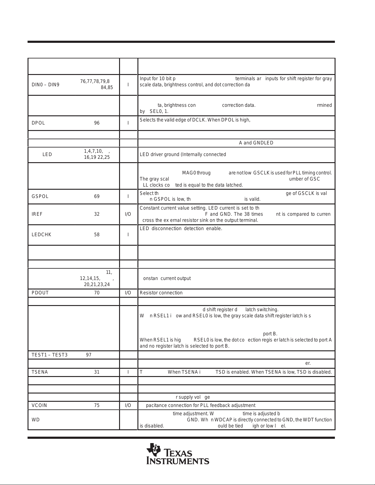
Input for 10 bit parallel data (port A). These terminals are inputs for shift register for gray
Á
Á
Á
ÁÁББББББББББББББББББББ
Á
Á
Á
Á
Á
Á
Á
Á
Á
Á
Á
ББББББББББББББББББББ
scale data, brightness control, and dot correction data. The register selected is determined
I
by RSEL0, 1.
ББББББББББББББББББББ
Output for 10 bit parallel data (port A). These terminals are outputs for shift register for gray
scale data, brightness control, and dot correction data. The register selected is determined
O
ББББББББББББББББББББ
by RSEL0, 1.
Selects the valid edge of DCLK. When DPOL is high, the rising edge of DCLK is valid. When
I
DPOL is low, the falling edge of DCLK is valid.
Analog ground (Internally connected to GNDLOG and GNDLED)
Logic ground (Internally connected to GNDANA and GNDLED)
LED driver ground (Internally connected to GNDANA and GNDLED)
Clock input for gray scale. When MAG0 through MAG2 are all low, GSCLK is used for pulse
width control. When MAG0 through MAG2 are not low, GSCLK is used for PLL timing control.
I
ББББББББББББББББББББ
The gray scale display is accomplished by lighting the LED until the number of GSCLK or
PLL clocks counted is equal to the data latched.
ББББББББББББББББББББ
Select the valid edge of GSCLK. When GSPOL is high, the rising edge of GSCLK is valid.
I
When GSPOL is low, the falling edge of GSCLK is valid.
Constant current value setting. LED current is set to the desired value by connecting an
external resistor between IREF and GND. The 38 times current is compared to current
I/O
ББББББББББББББББББББ
across the external resistor sink on the output terminal.
LED disconnection detection enable. When LEDCHK is high, the LED disconnection
ББББББББББББББББББББ
detection is enabled and XDOWN2 is valid. When LEDCHK is low, the LED disconnection
I
detection is disabled.
ББББББББББББББББББББ
PLL multiple ratio setting. The clock frequency generated by PLL referenced to GSCLK is
I
set .
No internal connection
O
Constant current output
ББББББББББББББББББББ
I/O
Resistor connection for PLL feedback adjustment
I/O
Resistor connection for PLL oscillation frequency setting
Input/output port selection and shift register data latch switching.
When RSEL1 is low and RSEL0 is low, the gray scale data shift register latch is selected to
ББББББББББББББББББББ
port A, and the dot correction register latch is selected to port B.
ББББББББББББББББББББ
When RSEL1 is low and RSEL0 is high, the brightness control register latch is selected to
I
port A, and the dot correction register latch is selected to port B.
ББББББББББББББББББББ
When RSEL1 is high and RSEL0 is low, the dot correction register latch is selected to port A
ББББББББББББББББББББ
and no register latch is selected to port B.
I
TEST. Factory test terminal. These terminals should be connected to GND.
Heat sink pad. This pad is connected to the lowest potential IC or thermal layer.
I
TSD enable. When TSENA is high, TSD is enabled. When TSENA is low, TSD is disabled.
Analog power supply voltage
Logic power supply voltage
LED driver power supply voltage
I/O
Capacitance connection for PLL feedback adjustment
WDT detection time adjustment. WDT detection time is adjusted by connecting a capacitor
between WDCAP and GND. When WDCAP is directly connected to GND, the WDT function
I/O
ББББББББББББББББББББ
is disabled. In this case, WDTRG should be tied to high or low level.
6
POST OFFICE BOX 655303 • DALLAS, TEXAS 75265
I/O
DESCRIPTION
Á
Á
Á
Á
ÁÁ
ÁÁ
ÁÁ
Á
Á
Á
Á
ÁÁ
ÁÁ
Á
Á
Á
ÁÁ
ÁÁ
Á
Á
Á
ÁÁ
ÁÁ
Á
Á
Á
ÁÁ
ÁÁ
Á
Á
Á
ÁÁ
ÁÁ
Á
Á
Á
ÁÁ
ÁÁ
Á
Á
Á
ÁÁ
ÁÁ
Á
Á
Á
ÁÁ
ÁÁ
Á
TERMINAL
NAME NO.
ÁÁÁÁ
WDTRG
ÁÁÁÁ
XDCLAT
ÁÁÁÁ
XDOWN1
ÁÁÁÁ
XDOWN2
ÁÁÁÁ
XDPOUT
XDWN2TST
ÁÁÁÁ
XENABLE
ÁÁÁÁ
XGSOUT
ÁÁÁÁ
XLATCH
ÁÁÁÁ
XOE
ÁÁÁÁ
XPOUT
ÁÁÁÁ
56
ÁÁÁÁ
61
ÁÁÁÁ
55
ÁÁÁÁ
54
ÁÁÁÁ
29
27
ÁÁÁÁ
66
ÁÁÁÁ
52
ÁÁÁÁ
63
ÁÁÁÁ
65
ÁÁÁÁ
51
LED DRIVER
SLLS402 – DECEMBER 1999
Terminal Functions (Continued)
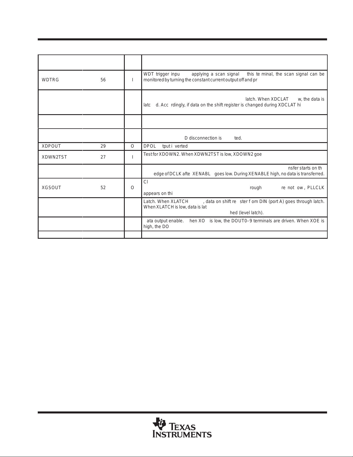
WDT trigger input. By applying a scan signal to this terminal, the scan signal can be
ББББББББББББББББББББ
monitored by turning the constant current output off and protecting the LED from the damage
I
of burning when the scan signal stops during the constant period designed.
ББББББББББББББББББББ
Data latch for dot correction. When XDCLAT is high, data on the shift register for dot
correction data from DCDIN (port B) goes through latch. When XDCLAT is low, the data is
I
ББББББББББББББББББББ
latched. Accordingly , if data on the shift register is changed during XDCLAT high, the new
value is latched (level latch).
Shutdown. XDOWN1 is configured as open collector. It goes low when the constant current
O
ББББББББББББББББББББ
output is shut down by the WDT or TSD function.
LED disconnection detection output. XDOWN2 is configured as open collector. XDOWN2
O
goes low when a LED disconnection is detected.
ББББББББББББББББББББ
O
DPOL output inverted
T est for XDOWN2. When XDWN2TST is low, XDOWN2 goes low . (This terminal is internally
I
ББББББББББББББББББББ
pulled up with 50 kΩ)
DCLK enable. When XENABLE is low, data transfer is enabled. Data transfer starts on the
I
valid edge of DCLK after XENABLE goes low. During XENABLE high, no data is transferred.
ББББББББББББББББББББ
Clock output for gray scale. When MAG0 through MAG2 are all low, a clock with GSCLK
inverted appears on this terminal. When MAG0 through MAG2 are not low., PLLCLK
O
ББББББББББББББББББББ
appears on this terminal.
Latch. When XLATCH is high, data on shift register from DIN (port A) goes through latch.
When XLATCH is low , data is latched. Accordingly , if the data on the shift register is changed
I
ББББББББББББББББББББ
during XLA TCH high, this new value is latched (level latch).
Data output enable. When XOE is low, the DOUT0–9 terminals are driven. When XOE is
I
high, the DOUT0–9 terminals go to a high-impedance state.
ББББББББББББББББББББ
O
GSPOL output inverted
TLC5911
POST OFFICE BOX 655303 • DALLAS, TEXAS 75265
7
TLC5911
Á
Á
Á
Á
Á
Á
Á
Á
Á
Á
Á
Á
Á
Á
Á
Á
Á
Á
Á
Á
Á
Á
Á
Á
Á
Á
Á
Á
Á
Á
Á
Á
mA
LED DRIVER
SLLS402 – DECEMBER 1999
absolute maximum ratings over operating free-air temperature (unless otherwise noted)
Logic supply voltage, V
CC(LOG)
Supply voltage for constant current circuit, V
Analog supply voltage, V
Output current (DC), I
CC(ANA)
OL(C)
– 0.3 V to 7 V. . . . . . . . . . . . . . . . . . . . . . . . . . . . . . . . . . . . . . . . . . . . . . . . . . . . .
CC(LED)
– 0.3 V to 7 V. . . . . . . . . . . . . . . . . . . . . . . . . . . . . . . . . . .
– 0.3 V to 7 V. . . . . . . . . . . . . . . . . . . . . . . . . . . . . . . . . . . . . . . . . . . . . . . . . . . .
85 mA. . . . . . . . . . . . . . . . . . . . . . . . . . . . . . . . . . . . . . . . . . . . . . . . . . . . . . . . . . . . . . .
†
Input voltage range, VI – 0.3 V to VCCLOG + 0.3 V. . . . . . . . . . . . . . . . . . . . . . . . . . . . . . . . . . . . . . . . . . . . . . . . .
Output voltage range, V
(DOUT)
Output voltage range, VO and V
Storage temperature range, T
, V
(DCDOUT)
(XDOWNn)
–40°C to 150°C. . . . . . . . . . . . . . . . . . . . . . . . . . . . . . . . . . . . . . . . . . . . . . . . . . .
str
, V
(BOUT)
, V
(XPOUT)
and V
(XGSOUT)
– 0.3 V to VCCLOG + 0.3 V
– 0.3 V to 16 V. . . . . . . . . . . . . . . . . . . . . . . . . . . . . . . . . . . . . . . . . . .
Continuous total power dissipation at (or below) TA = 25°C 4.7 W. . . . . . . . . . . . . . . . . . . . . . . . . . . . . . . . . . . .
Power dissipation rating at (or above) TA = 25°C 38.2m W/°C. . . . . . . . . . . . . . . . . . . . . . . . . . . . . . . . . . . . . . .
†
Stresses beyond those listed under “absolute maximum ratings” may cause permanent damage to the device. These are stress ratings only, and
functional operation of the device at these or any other conditions beyond those indicated under “recommended operating conditions” is not
implied. Exposure to absolute-maximum-rated conditions for extended periods may affect device reliability.
NOTE 1: All voltage values are with respect to GNDLOG terminal.
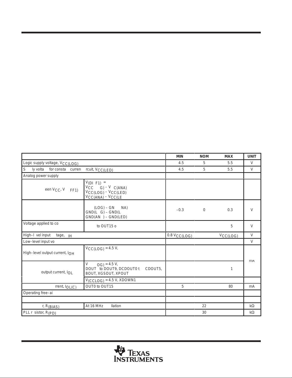
recommended operating conditions
dc characteristics
Logic supply voltage, V
CC(LOG)
Supply voltage for constant current circuit, V
Analog power supply, V
ББББББББ
Voltage between VCC, V
ББББББББ
Voltage between GND, V
ББББББББ
ББББББББ
Voltage applied to constant current
output, V
O
High–level input voltage, V
Low–level input voltage, V
High–level output current, I
ББББББББ
ББББББББ
Low–level output current, I
Constant output current, I
Operating free–air temperature range, T
PLL capacitance, C
PLL resistor, R
PLL resistor, R
(BIAS)
(PD)
CC(ANA)
(VCO)
(DIFF1)
(DIFF2)
IH
IL
OH
OL
OL(C)
V
(DIFF1)
V
CC(LOG)
ББББББББББ
V
CC(LOG)
ББББББББББ
V
CC(ANA)
V
(DIFF2)
GND(LOG) – GND(ANA)
ББББББББББ
GND(LOG) – GND(LED)
GND(ANA) – GND(LED)
ББББББББББ
OUT0 to OUT15 off
V
CC(LOG)
DOUT0 to DOUT9, DCDOUT0 to DCDOUT5,
ББББББББББ
BOUT, XGSOUT, XPOUT
V
CC(LOG)
DOUT0 to DOUT9, DCDOUT0 to DCDOUT5,
ББББББББББ
BOUT, XGSOUT, XPOUT
V
(CCLOG)
OUT0 to OUT15
A
At 16 MHz oscillation
CC(LED)
=
– V
CC(ANA)
– V
CC(LED)
– V
CC(LED)
=
= 4.5 V,
= 4.5 V,
= 4.5 V, XDOWN1, XDOWN2
MIN
4.5
4.5
4.5
ÁÁÁ
–0.3
ÁÁÁ
–0.3
ÁÁÁ
ÁÁÁ
0.8 V
CC(LOG)
GND(LOG)
ÁÁÁÁÁÁÁÁÁÁ
ÁÁÁÁÁÁÁÁÁÁ
5
–20
NOM
5
5
5
ÁÁ
0
ÁÁ
0
ÁÁ
ÁÁ
1
22
30
MAX
5.5
5.5
5.5
ÁÁÁ
0.3
ÁÁÁ
0.3
ÁÁÁ
ÁÁÁ
15
V
CC(LOG)
0.2 V
CC(LOG)
–1
1
5
80
85
UNIT
V
V
V
Á
V
Á
V
Á
Á
V
V
V
Á
Á
mA
mA
°C
µF
kΩ
kΩ
8
POST OFFICE BOX 655303 • DALLAS, TEXAS 75265
DCLK, DCCLK clock frequenc
f
MH
Á
Á
Á
Á
Á
Á
Á
Á
Á
Á
Á
Á
Á
Á
Á
Á
Á
Á
Á
Á
Á
Á
Á
Á
Á
Á
Á
Á
Á
Á
Á
Á
Á
Á
Á
Á
Á
Á
Á
Á
Á
Á
Á
Á
Á
Á
Á
Á
Á
Á
Á
Á
Á
Á
Á
Á
Á
Á
Á
Á
Á
Á
Á
Á
Á
Á
Á
Á
Á
Á
Á
Á
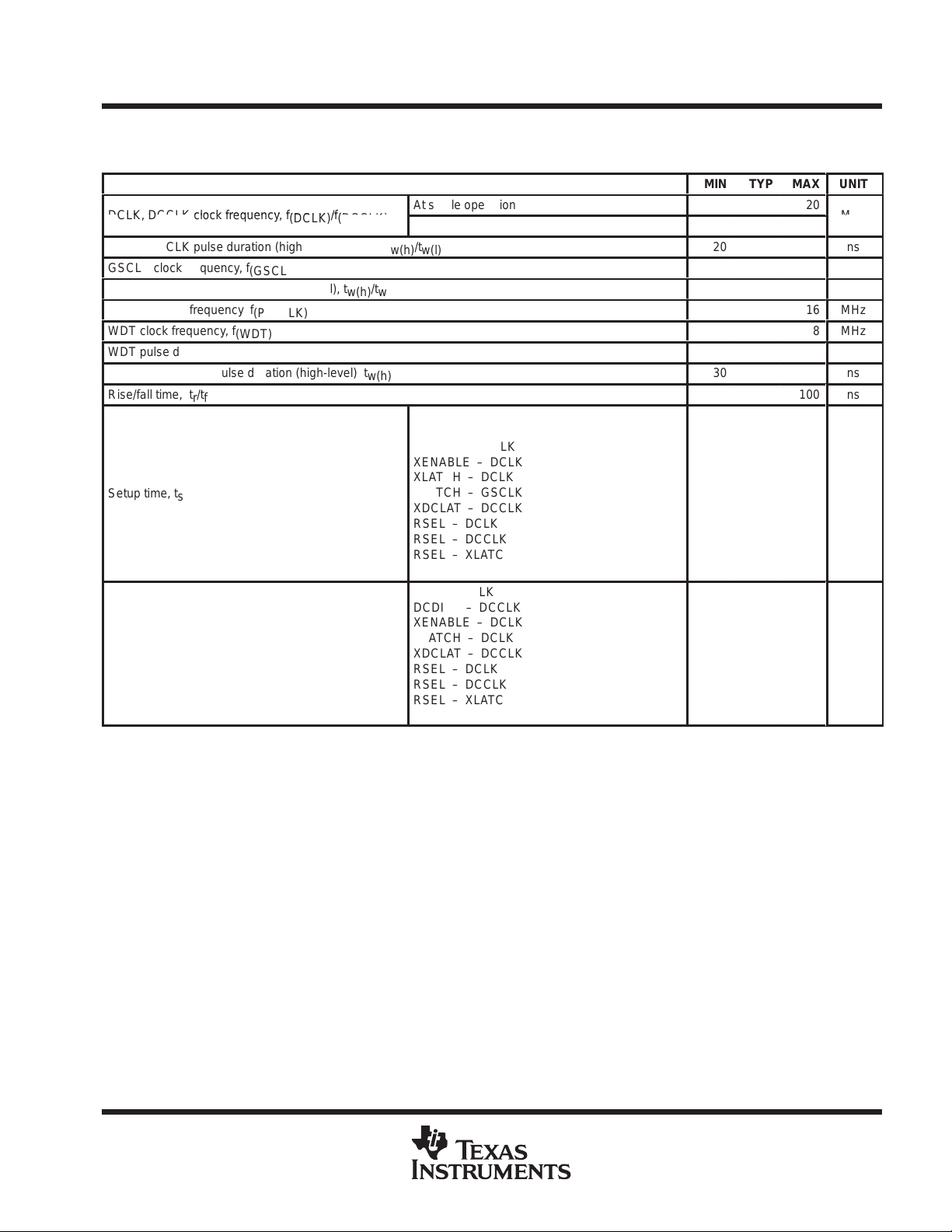
recommended operating conditions (continued)
TLC5911
LED DRIVER
SLLS402 – DECEMBER 1999
ac characteristics, V
CC(LOG)
= V
CC(ANA)
y,
(DCLK)/f(DCCLK)
DCLK, DCCLK pulse duration (high- or low-level), t
GSCLK clock frequency, f
GSCLK pulse duration (high- or low-level), t
PLLCLK clock frequency, f
WDT clock frequency, f
WDT pulse duration (high- or low-level), t
(GSCLK)
w(h)/tw(l)
(PLLCLK)
(WDT)
w(h)/tw(l)
XLATCH, XDCLAT pulse duration (high-level), t
Rise/fall time, tr/t
ББББББББББББ
ББББББББББББ
ББББББББББББ
Setup time, t
ББББББББББББ
ББББББББББББ
ББББББББББББ
ББББББББББББ
ББББББББББББ
ББББББББББББ
Hold time, t
ББББББББББББ
ББББББББББББ
ББББББББББББ
f
su
h
= V
CC(LED)
At single operation
At cascade operation
w(h)/tw(l)
w(h)
DINn – DCLK
DCDINn – DCCLK
BLANK – GSCLK
XENABLE – DCLK
XLATCH – DCLK
XLATCH – GSCLK
XDCLAT – DCCLK
RSEL – DCLK
RSEL – DCCLK
RSEL – XLATCH
RSEL – XDCLAT
DINn – DCLK
DCDINn – DCCLK
XENABLE – DCLK
XLATCH – DCLK
XDCLAT – DCCLK
RSEL – DCLK
RSEL – DCCLK
RSEL – XLATCH
RSEL – XDCLAT
= 4.5 V to 5.5 V, T A = – 20 to 85°C (unless otherwise noted)
MIN
TYP
20
40
40
30
ББББББББББ
ББББББББББ
ББББББББББ
ББББББББББ
ББББББББББ
ББББББББББ
ББББББББББ
ББББББББББ
ББББББББББ
ББББББББББ
ББББББББББ
ББББББББББ
Á
Á
Á
Á
Á
Á
Á
Á
Á
Á
Á
Á
10
15
10
10
10
10
15
30
15
15
15
20
30
20
20
20
20
10
5
Á
5
Á
Á
Á
Á
Á
Á
Á
Á
Á
Á
Á
MAX
100
Á
Á
Á
Á
Á
Á
Á
Á
Á
Á
Á
Á
20
15
16
UNIT
z
ns
8
MHz
ns
MHz
8
MHz
ns
ns
ns
Á
Á
Á
ns
Á
Á
Á
Á
Á
Á
ns
Á
Á
Á
POST OFFICE BOX 655303 • DALLAS, TEXAS 75265
9
 Loading...