TEXAS INSTRUMENTS TLC5905 Technical data
D
Drive Capability and Output Counts:
– 80 mA (Current Sink) × 16 Bits
– 120 mA (Current Sink) × 8 Bits
D
Constant Current Output Range:
– 5 mA to 80 mA/10 mA to 120 mA
(Selectable by MODE Terminal) (Current
Value Setting for All Output Terminals
Using External Resistor and Internal
Brightness Control Register)
D
Constant Current Accuracy ±4% (Maximum
Error Between Bits)
D
Voltage Applied to Constant Current Output
Terminals:
– Minimum 0.4 V (Output Current 5 mA to
40 mA)
– Minimum 0.7 V (Output Current 40 mA to
80 mA)
D
256 Gray Scale Display:
– Pulse Width Control 256 Steps
D
Brightness Adjustment:
– Output Current Adjustment for 32 Steps
(Adjustment for Brightness Deviation
Between LED Modules)
– 8 Steps Brightness Control by 8 Times
Speed Gray Scale Control Clock
(Brightness Adjustment for Panel)
D
Error Output Signal Check:
– Check Error Output Signal Line Such as
Protection Circuit When Operating
D
Data Output Timing Selectable:
– Select Data Output Timing for Shift
Register Relative to Clock
description
LED DRIVER
SLLS401 – NOVEMBER 1999
D
OVM (Output Voltage Monitor):
– Monitor Voltage on Constant Current
Output Terminals (Detect LED
Disconnection and Short Circuit)
D
WDT (Watchdog Timer):
– Turn Output Off When Scan Signal
Stopped
D
TSD (Thermal Shut Down):
– Turn Output Off When Junction
T emperature Exceeds Limit
D
Data Input:
– Clock Synchronized 1 Bit Serial Input
(Shmitt-Triggered Input)
D
Data Output:
– Clock Synchronized 1 Bit Serial Output
(3-State Output)
D
Input Signal Level:
– CMOS Level
D
Power Supply Voltage . . . 4.5 V to 5.5 V
D
Maximum Output Voltage . . . 17 V
D
Data Transfer Rate . . . 15 MHz (Max
D
Gray Scale Clock Frequency ...8 MHz
(Max)
D
Operating Free-Air Temperature Range
–20°C to 85°C
D
64-Pin HTQFP Package (PD = 4.9 W,
T
= 25°C)
A
TLC5905
The TLC5905 is a constant current driver that incorporates shift register, data latch, constant current circuitry
with a current value adjustable and 256 gray scale display that uses pulse width control. The output current can
be selected as maximum 80 mA with 16 bits or 120 mA with 8 bit. The current value of the constant current output
is set by one external resistor. After this device is mounted on a printed-circuit board (PCB), the brightness
deviation between LED modules (ICs) can be adjusted using an external data input, and the brightness control
for the panel can be accomplished by the brightness adjustment circuitry. Also, the device incorporates the
output voltage monitor (OVM) used for LED open detection (LOD) by monitoring constant current output.
Moreover, the device incorporates watchdog timer (WDT) circuitry , which turns constant current output off when
the scan signal stops during dynamic scanning operation, and thermal shutdown (TSD) circuitry, which turns
constant current output off when the junction temperature exceeds the limit.
Please be aware that an important notice concerning availability, standard warranty, and use in critical applications of
Texas Instruments semiconductor products and disclaimers thereto appears at the end of this data sheet.
PRODUCTION DATA information is current as of publication date.
Products conform to specifications per the terms of Texas Instruments
standard warranty. Production processing does not necessarily include
testing of all parameters.
POST OFFICE BOX 655303 • DALLAS, TEXAS 75265
Copyright 1999, Texas Instruments Incorporated
1

TLC5905
LED DRIVER
SLLS401 – NOVEMBER 1999
pin assignments
PAP PACKAGE
(TOP VIEW)
NC
OUT3
63 62 61 60 5964 58 56 55 5457
1
NC
OUT4
GNDLED
OUT5
OUT6
GNDLED
OUT7
OUT8
GNDLED
OUT9
OUT10
GNDLED
OUT11
NC
NC
NC
2
3
4
5
6
7
8
9
10
11
12
13
14
15
16
17 18
19
NC
OUT12
NC – No internal connection
GNDLED
OUT2
OUT1
21 22 23 24
20
OUT13
OUT14
GNDLED
GNDLED
OUT0NCNC
NC
OUT15
GNDLED
BCENA
GNDLOG
MODEVTSENANCSIN
53 52 51 50 49
25 26 27 28 29
IREF
CCLED
WDCAP
V
GNDANA
CCLOG
30 31 32
NC
CCANA
V
48
47
46
45
44
43
42
41
40
39
38
37
36
35
34
33
SOUT
MCENA
TEST2
SOMODE
GSCLK
BLANK
RSEL1
RSEL0
SCLK
XENABLE
XOE
WDTRG
XLATCH
XDOWN1
XDOWN2
TEST1
BOUT
GSOUT
2
POST OFFICE BOX 655303 • DALLAS, TEXAS 75265
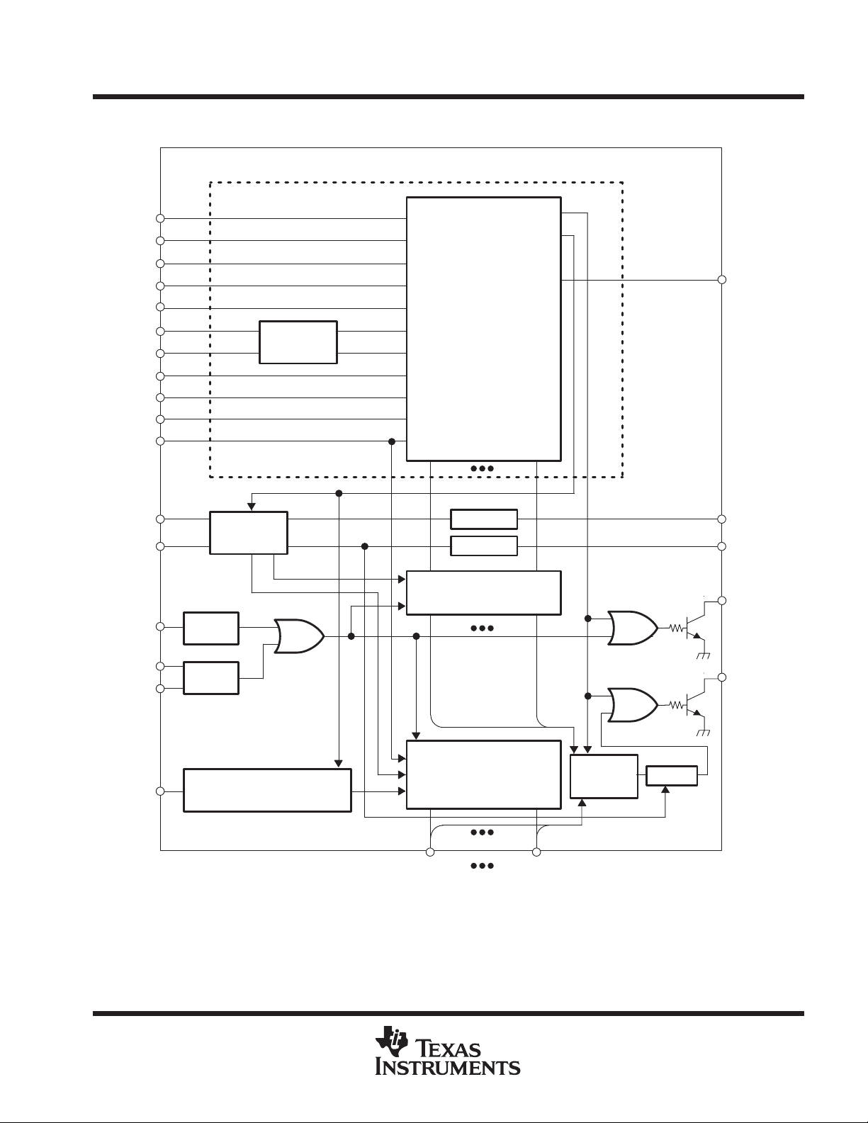
functional block diagram
TLC5905
LED DRIVER
SLLS401 – NOVEMBER 1999
Shift Register and Data Latch
MCENA
BCENA
RSEL0
RSEL1
SIN
XENABLE
SCLK
SOMODE
XOE
XLATCH
MODE
GSCLK
BLANK
TSENA
Gray Scale
TSD
8 bits
Counter
SCLK
Controller
OVM
Shift Register
Data Latch
Brightness Control
Shift Register
Data Latch
Gray Scale Control
Shift Register
Data Latch
DELEY
DELEY BOUT
16 x 8 bits
Comparator
SOUT
GSOUT
XDOWN1
WDTRG
WDCAP
IREF
NOTE: All the input terminals are with Schmitt-triggered inverter except IREF and WDCAP.
WDT
Current Reference
Circuit
Constant Current Driver
16 bits
OUT0 OUT15
16 bits
OVM Comp
XDOWN2
LATCH
POST OFFICE BOX 655303 • DALLAS, TEXAS 75265
3
TLC5905
LED DRIVER
SLLS401 – NOVEMBER 1999
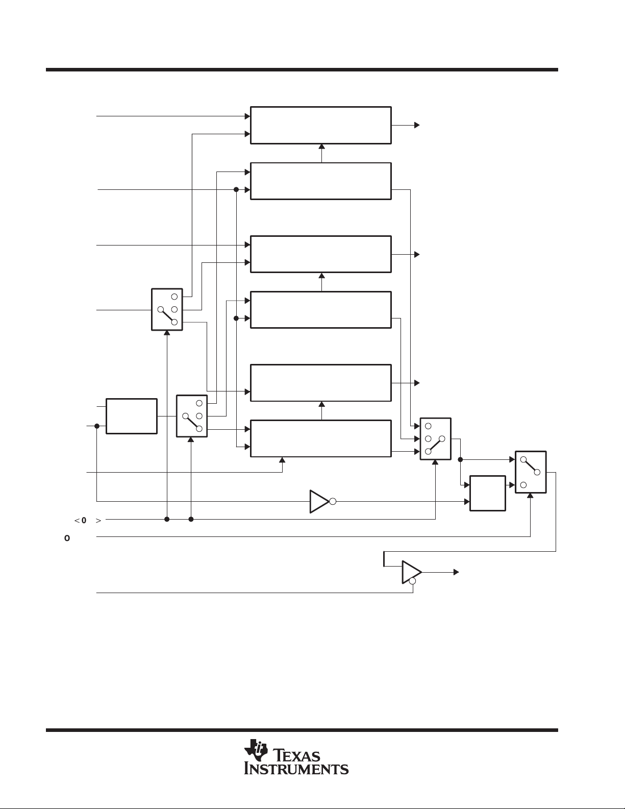
functional block diagram for shift register and data latch
MCENA
SIN
BCENA
XLATCH
XENABLE
SCLK
SCLK
Controller
OVM Data Latch
(1 x 8 bit)
OVM Shift Register
(8 x 1 bit)
Brightness Control Data Latch
(1 x 8 bit)
Brightness Control Shift Register
(8 x 1 bit)
Gray Scale Control Data Latch
(16 x 8 bit)
Gray Scale Control Shift Register
(128 x 1 bit / 64 x 1 bit)
16 bit OVM Comparator
XDOWN1, 2 Output Driver
Constant Current Driver Control
Gray Scale Clock Counter
16 x 8 bit Data Comparator
MODE
RSELt0–1
SOMODE
NOTE: Enclosed in ( ) is dependent on MODE pin selection.
u
XOE
(see Note)
1 bit
S/R
SOUT
4
POST OFFICE BOX 655303 • DALLAS, TEXAS 75265
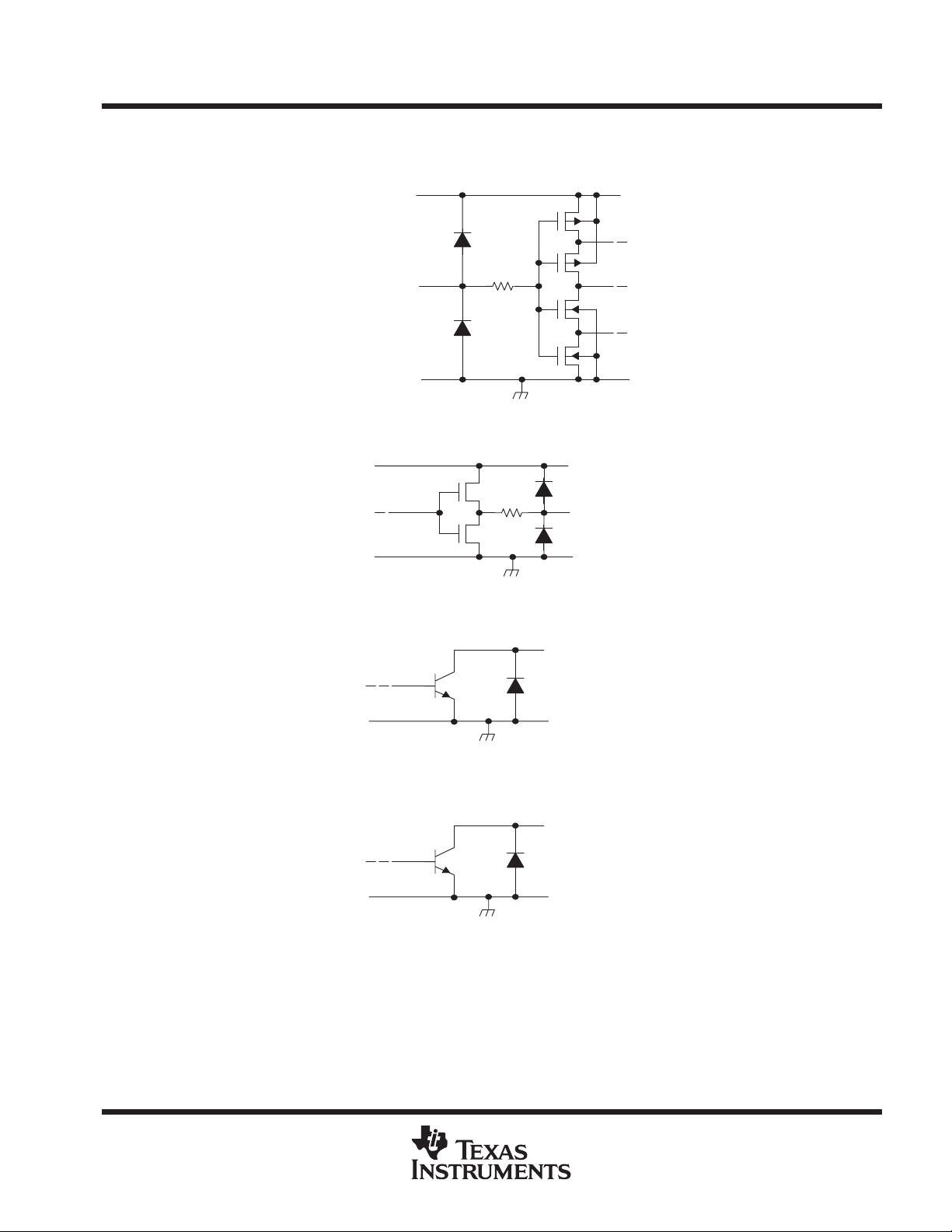
equivalent input and output schematic diagrams
TLC5905
LED DRIVER
SLLS401 – NOVEMBER 1999
Input
SOUT, GSOUT, BOUT
XDOWN1, XDOWN2
VCCLOG
INPUT
GNDLOG
VCCLOG
OUTPUT
GNDLOG
OUTn
XDOWN1, XDOWN2
GNDLOG
OUTn
GNDLED
POST OFFICE BOX 655303 • DALLAS, TEXAS 75265
5
TLC5905
I/O
DESCRIPTION
Á
Á
Á
Á
Á
Á
Á
Á
Á
Á
Á
Á
Á
Á
Á
Á
Á
Á
Á
Á
Á
Á
Á
Á
Á
Á
Á
Á
Á
Á
Á
Á
Á
Á
Á
Á
Á
Á
Á
Á
Á
Á
Á
Á
Á
Á
Á
Á
Á
Á
Á
Á
Á
Á
Á
Á
Á
Á
Á
Á
Á
Á
Á
LED DRIVER
SLLS401 – NOVEMBER 1999
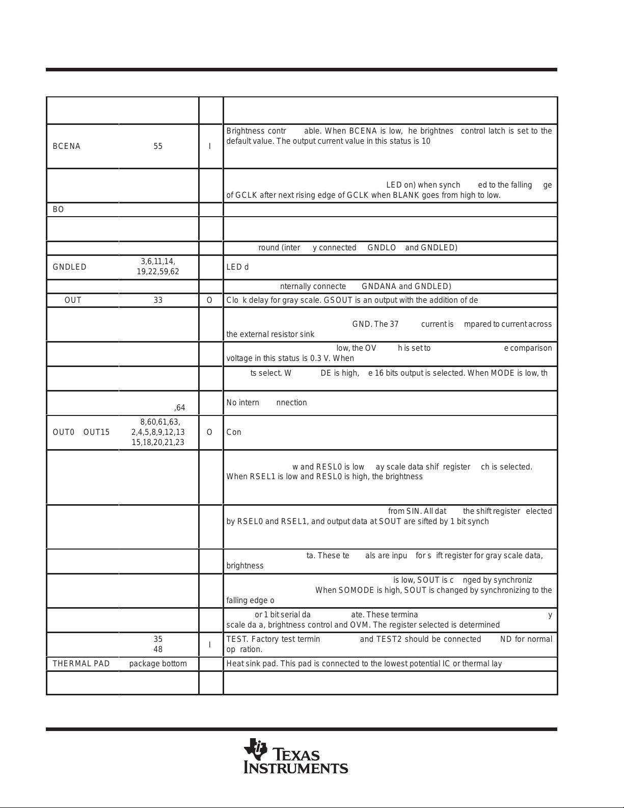
TERMINAL
NAME NO.
ÁÁÁÁ
BCENA
ÁÁÁÁ
ÁÁÁÁ
BLANK
BOUT
GSCLK
ÁÁÁÁ
GNDANA
GNDLED
GNDLOG
GSOUT
IREF
ÁÁÁÁ
MCENA
ÁÁÁÁ
MODE
NC
ÁÁÁÁ
OUT0 – OUT15
ÁÁÁÁ
ÁÁÁÁ
RSEL0
RSEL1
ÁÁÁÁ
ÁÁÁÁ
SCLK
ÁÁÁÁ
ÁÁÁÁ
SIN
SOMODE
ÁÁÁÁ
SOUT
ÁÁÁÁ
TEST1
TEST2
THERMAL PAD
TSENA
ÁÁÁÁ
ÁÁÁÁ
ÁÁÁÁ
ÁÁÁÁ
ÁÁÁÁ
ÁÁÁÁ
ÁÁÁÁ
1,7,10,16,17,24,
ÁÁÁÁ
29,50,56,57,64
2,4,5,8,9,12,13
ÁÁÁÁ
15,18,20,21,23
ÁÁÁÁ
ÁÁÁÁ
ÁÁÁÁ
ÁÁÁÁ
ÁÁÁÁ
ÁÁÁÁ
ÁÁÁÁ
package bottom
ÁÁÁÁ
55
45
34
46
28
3,6,11,14,
19,22,59,62
54
33
25
31
53
58,60,61,63,
43
44
42
49
47
32
35
48
51
Terminal Functions
Brightness control enable. When BCENA is low, the brightness control latch is set to the
Á
Á
Á
Á
I/O
Á
Á
ÁÁББББББББББББББББББББ
Á
Á
Á
Á
Á
Á
Á
Á
Á
ББББББББББББББББББББ
default value. The output current value in this status is 100% of the value set by an external
I
resistor. The frequency division ratio of GSCLK is1/1. When BCENA is high, writing to
ББББББББББББББББББББ
brightness control latch is enabled.
Blank(Light off). When BLANK is high, all the output of the constant current driver is turned
ББББББББББББББББББББ
off. The constant current output is turned on (LED on) when synchronized to the falling edge
I
of GCLK after next rising edge of GCLK when BLANK goes from high to low.
O
Blank signal delay. BOUT is an output with the addition of delay time to BLANK.
Clock input for gray scale. The gray scale display is accomplished by lighting the LED on until
I
ББББББББББББББББББББ
the number of GSCLK counted is equal to data latched.
Analog ground (internally connected to GNDLOG and GNDLED)
LED driver ground (internally connected to GNDANA and GNDLOG)
Logic ground (internally connected to GNDANA and GNDLED)
O
Clock delay for gray scale. GSOUT is an output with the addition of delay time to GSCLK.
Constant current value setting. LED current is set to the desired value by connecting an
external resistor between IREF and GND. The 37 times current is compared to current across
ББББББББББББББББББББ
the external resistor sink on the output terminal.
OVM enable. When MCENA is low, the OVM latch is set to the default value. The comparison
I
ББББББББББББББББББББ
voltage in this status is 0.3 V. When MCENA is high, writing to OVM latch is enabled.
8/16 bits select. When MODE is high, the 16 bits output is selected. When MODE is low, the
I
8 bits output is selected.
No internal connection
O
Constant current output
ББББББББББББББББББББ
Shift register data latch switching.
ББББББББББББББББББББ
When RSEL1 is low and RESL0 is low, gray scale data shift register latch is selected.
When RSEL1 is low and RESL0 is high, the brightness control register latch is selected.
I
ББББББББББББББББББББ
When RSEL1 is high and RSEL0 is low, the OVM register latch is selected.
When RSEL1 is high and RSEL0 high, no register latch is selected.
ББББББББББББББББББББ
Clock input for data transfer. The input data is from SIN. All data on the shift register selected
by RSEL0 and RSEL1, and output data at SOUT are sifted by 1 bit synchronizing to SCLK.
I
ББББББББББББББББББББ
The data except the SOUT is synchronized to the rising edge. The edge for data from SOUT
is determined by the level of SOMODE.
ББББББББББББББББББББ
Input for 1 bit serial data. These terminals are inputs for shift register for gray scale data,
I
brightness control and OVM. The register selected is determined by RSEL0, 1.
Timing select for data output. When SOMODE is low , SOUT is changed by synchronizing to
the rising edge of SCLK. When SOMODE is high, SOUT is changed by synchronizing to the
I
ББББББББББББББББББББ
falling edge of SCLK.
Output for 1 bit serial data with 3–state. These terminals are outputs for shift register for gray
O
ББББББББББББББББББББ
scale data, brightness control and OVM. The register selected is determined by RSEL0, 1.
TEST. Factory test terminal. TEST1 and TEST2 should be connected to GND for normal
I
operation.
Heat sink pad. This pad is connected to the lowest potential IC or thermal layer.
TSD (thermal shutdown) enable. When TSENA is high, TSD is enabled. When TSENA is low,
I
ББББББББББББББББББББ
TSD is disabled.
6
POST OFFICE BOX 655303 • DALLAS, TEXAS 75265
I/O
DESCRIPTION
Á
Á
Á
Á
Á
Á
Á
Á
Á
Á
Á
Á
Á
Á
Á
Á
Á
Á
Á
Á
Á
Á
Á
Á
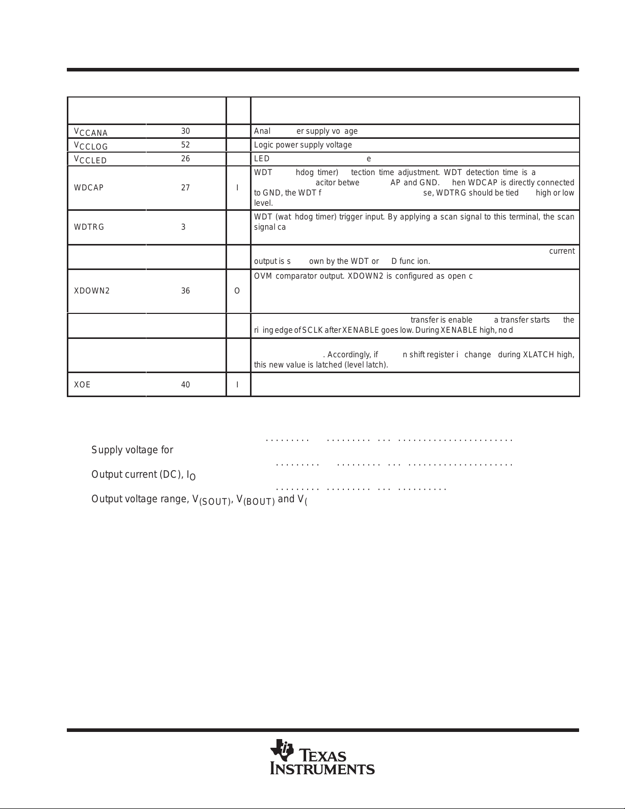
TERMINAL
NAME NO.
V
CCANA
V
CCLOG
V
CCLED
ÁÁÁÁ
WDCAP
ÁÁÁÁ
WDTRG
ÁÁÁÁ
XDOWN1
ÁÁÁÁ
XDOWN2
ÁÁÁÁ
XENABLE
ÁÁÁÁ
XLATCH
ÁÁÁÁ
XOE
ÁÁÁÁ
30
52
26
ÁÁÁÁ
27
ÁÁÁÁ
39
ÁÁÁÁ
37
ÁÁÁÁ
36
ÁÁÁÁ
41
ÁÁÁÁ
38
ÁÁÁÁ
40
ÁÁÁÁ
LED DRIVER
SLLS401 – NOVEMBER 1999
Terminal Functions (Continued)
Analog power supply voltage
Logic power supply voltage
LED driver power supply voltage
WDT (watchdog timer) detection time adjustment. WDT detection time is adjusted by
connecting a capacitor between WDCAP and GND. When WDCAP is directly connected
ББББББББББББББББББББ
I
to GND, the WDT function is disabled. In this case, WDTRG should be tied to a high or low
ББББББББББББББББББББ
level.
WDT (watchdog timer) trigger input. By applying a scan signal to this terminal, the scan
signal can be monitored by turning the constant current output off and protecting the LED
I
ББББББББББББББББББББ
from damage by burning when the scan signal is stopped during constant period designed.
Shutdown. XDOWN1 is configured as an open collector. It goes low when constant current
O
output is shut down by the WDT or TSD function.
ББББББББББББББББББББ
OVM comparator output. XDOWN2 is configured as open collector. It monitors terminal
voltage when constant current output is turned on. XDOWN2 goes low when this voltage is
O
ББББББББББББББББББББ
lower than the level selected by the OVM latch. When BLANK is set high, the previous level
is held.
SCLK enable. When XENABLE is low, data transfer is enabled. Data transfer starts on the
I
ББББББББББББББББББББ
rising edge of SCLK after XENABLE goes low. During XENABLE high, no data is transferred.
Latch. When XLATCH is high, data on shift register goes through latch. When XLATCH is
low, data is latched. Accordingly, if data on shift register is changed during XLATCH high,
I
ББББББББББББББББББББ
this new value is latched (level latch).
Data output enable. When XOE is low, the SOUT terminal is drived. When XOE is high, the
I
ББББББББББББББББББББ
SOUT terminal goes to high-impedance state.
TLC5905
absolute maximum ratings over operating free-air temperature (unless otherwise noted)
Logic supply voltage, V
CC(LOG)
Supply voltage for constant current circuit, V
Analog supply voltage, V
Output current (DC), I
CC(ANA)
OL(C)
Input voltage range, VI – 0.3 V to V
Output voltage range, V
Output voltage range, V
(SOUT)
(OUTn)
Storage temperature range, T
– 0.3 V to 7 V. . . . . . . . . . . . . . . . . . . . . . . . . . . . . . . . . . . . . . . . . . . . . . . . . . . . .
CC(LED)
– 0.3 V to 7 V. . . . . . . . . . . . . . . . . . . . . . . . . . . . . . . . . . .
– 0.3 V to 7 V. . . . . . . . . . . . . . . . . . . . . . . . . . . . . . . . . . . . . . . . . . . . . . . . . . . .
90 mA. . . . . . . . . . . . . . . . . . . . . . . . . . . . . . . . . . . . . . . . . . . . . . . . . . . . . . . . . . . . . . .
, V
(BOUT)
and V
–40°C to 125°C. . . . . . . . . . . . . . . . . . . . . . . . . . . . . . . . . . . . . . . . . . . . . . . . . . .
stg
and V
(XDOWNn)
(GSOUT)
– 0.3 V to V
– 0.3 V to 18 V. . . . . . . . . . . . . . . . . . . . . . . . . . . . . . . . . . . . . . .
CC(LOG)
CC(LOG)
†
+ 0.3 V. . . . . . . . . . . . . . . . . . . . . . . . . . . . . . . . . . . . . . . . . . . . . . . . .
+ 0.3 V. . . . . . . . . . . . . . . . . . .
Continuous total power dissipation at (or below) TA = 25°C 4.9 W. . . . . . . . . . . . . . . . . . . . . . . . . . . . . . . . . . . . .
Power dissipation rating at (or above) TA = 25°C 39.4 mW/°C. . . . . . . . . . . . . . . . . . . . . . . . . . . . . . . . . . . . . . .
†
Stresses beyond those listed under “absolute maximum ratings” may cause permanent damage to the device. These are stress ratings only, and
functional operation of the device at these or any other conditions beyond those indicated under “recommended operating conditions” is not
implied. Exposure to absolute-maximum-rated conditions for extended periods may affect device reliability.
NOTE 1: All voltage values are with respect to GNDLOG terminal.
POST OFFICE BOX 655303 • DALLAS, TEXAS 75265
7
TLC5905
Á
Á
Á
Á
Á
Á
Á
Á
Á
Á
Á
Á
Á
Á
Á
Á
Á
Á
Á
Á
Á
mA
Low-level output current, I
SCLK clock frequenc
f
MH
GSCLK clock frequenc
f(
MH
GSCLK pulse duration (high or low level), t
ns
LED DRIVER
SLLS401 – NOVEMBER 1999
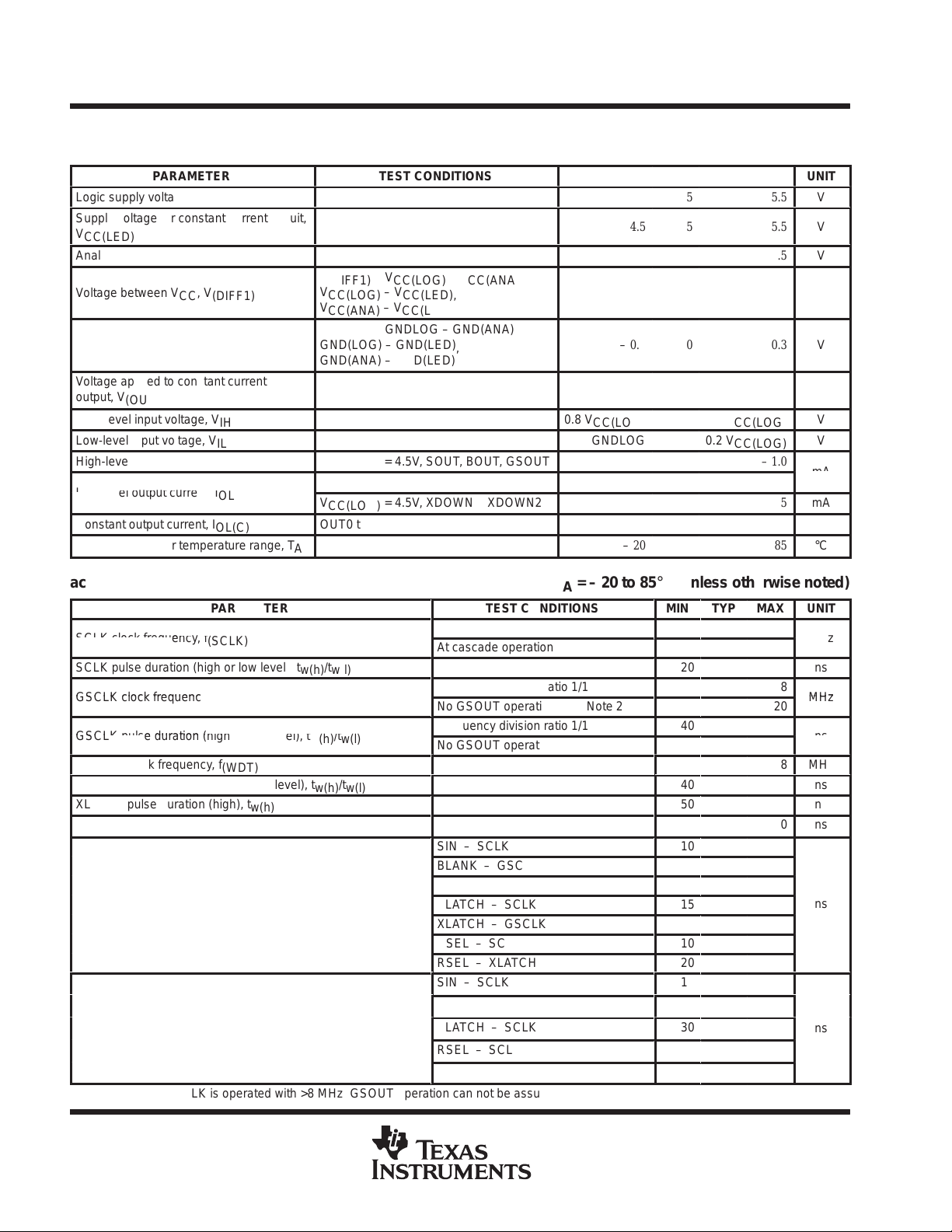
recommended operating conditions
dc characteristics
PARAMETER
Logic supply voltage, V
Supply voltage for constant current circuit,
ББББББББББ
V
CC(LED)
Analog power supply, V
Voltage between VCC, V
ББББББББББ
Voltage between GND, V
ББББББББББ
Voltage applied to constant current
output, V
ББББББББББ
(OUTn)
High-level input voltage, V
Low-level input voltage, V
High-level output current, I
p
Constant output current, I
Operating free–air temperature range, T
CC(LOG)
CC(ANA)
(DIFF1)
(DIFF2)
IH
IL
OH
OL
OL(C)
БББББББББÁÁÁÁ
V
(DIFF1)
V
CC(LOG)
БББББББББ
V
CC(ANA)
V
(DIFF2)
GND(LOG) – GND(LED),
БББББББББ
GND(ANA) – GND(LED)
OUT0 to OUT15 off
БББББББББ
V
CC(LOG)
V
CC(LOG)
V
CC(LOG)
OUT0 to OUT15
A
TEST CONDITIONS
= V
– V
– V
CC(LOG)
CC(LED),
CC(LED)
– V
CC(ANA)
= GNDLOG – GND(ANA)
= 4.5V, SOUT, BOUT, GSOUT
= 4.5V, SOUT, BOUT, GSOUT
= 4.5V, XDOWN1, XDOWN2
MIN
ÁÁÁ
ÁÁÁ
ÁÁÁÁÁÁÁÁÁ
0.8 V
CC(LOG)
GNDLOG
4.5
4.5
4.5
– 0.3
– 0.3
NOM
Á
Á
Á
5
5
ÁÁÁ
5
0
ÁÁÁ
0
ÁÁÁ
0.2 V
MAX
V
CC(LOG)
CC(LOG)
5
– 20
5.5
5.5
5.5
0.3
0.3
17
– 1.0
1.0
80
85
UNIT
V
V
Á
V
V
Á
V
Á
V
Á
V
V
5
mA
mA
°C
ac characteristics, V
CC(LOG)
PARAMETER
y,
(SCLK)
SCLK pulse duration (high or low level), t
y,
GSCLK)
p
WDTRG clock frequency, f
(WDT)
WDTRG pulse duration (high or low level), t
XLATCH pulse duration (high), t
Rise/fall time, tr/t
f
w(h)
= V
CC(ANA)
w(h)/tw(l)
w(h)/tw(l)
w(h)/tw(l)
= V
CC(LED)
= 4. 5 V to 5 . 5 V, T
TEST CONDITIONS
At single operation
At cascade operation (SOMODE = L)
Frequency division ratio 1/1
No GSOUT operation (see Note 2)
Frequency division ratio 1/1
No GSOUT operation (see Note 2)
SIN – SCLK
BLANK – GSCLK
XENABLE – SCLK
Setup time, t
su
XLATCH – SCLK
XLATCH – GSCLK
RSEL – SCLK
RSEL – XLATCH
SIN – SCLK
XENABLE – SCLK
Hold time, t
h
XLATCH – SCLK
RSEL – SCLK
RSEL – XLATCH
NOTE 2: When GSCLK is operated with >8 MHz, GSOUT operation can not be assured.
= – 20 to 85°C (u n l e s s o t h e r w i s e n o t e d)
A
MIN
TYP
MAX
UNIT
15
10
20
8
20
40
20
8
MHz
40
50
100
10
20
15
15
10
10
20
10
20
30
20
20
z
ns
z
ns
ns
ns
ns
ns
8
POST OFFICE BOX 655303 • DALLAS, TEXAS 75265
Á
Á
Á
Á
Á
VOLLow-level output voltage
V
Á
Á
Á
Á
Á
(LOG)
y(g)
I
Supply current (analog)
mA
Á
Á
Á
Á
Á
Á
Á
Á
Á
Á
Á
Á
Á
()
Á
Á
Á
Á
Á
Á
Á
Á
Á
Á
Á
Á
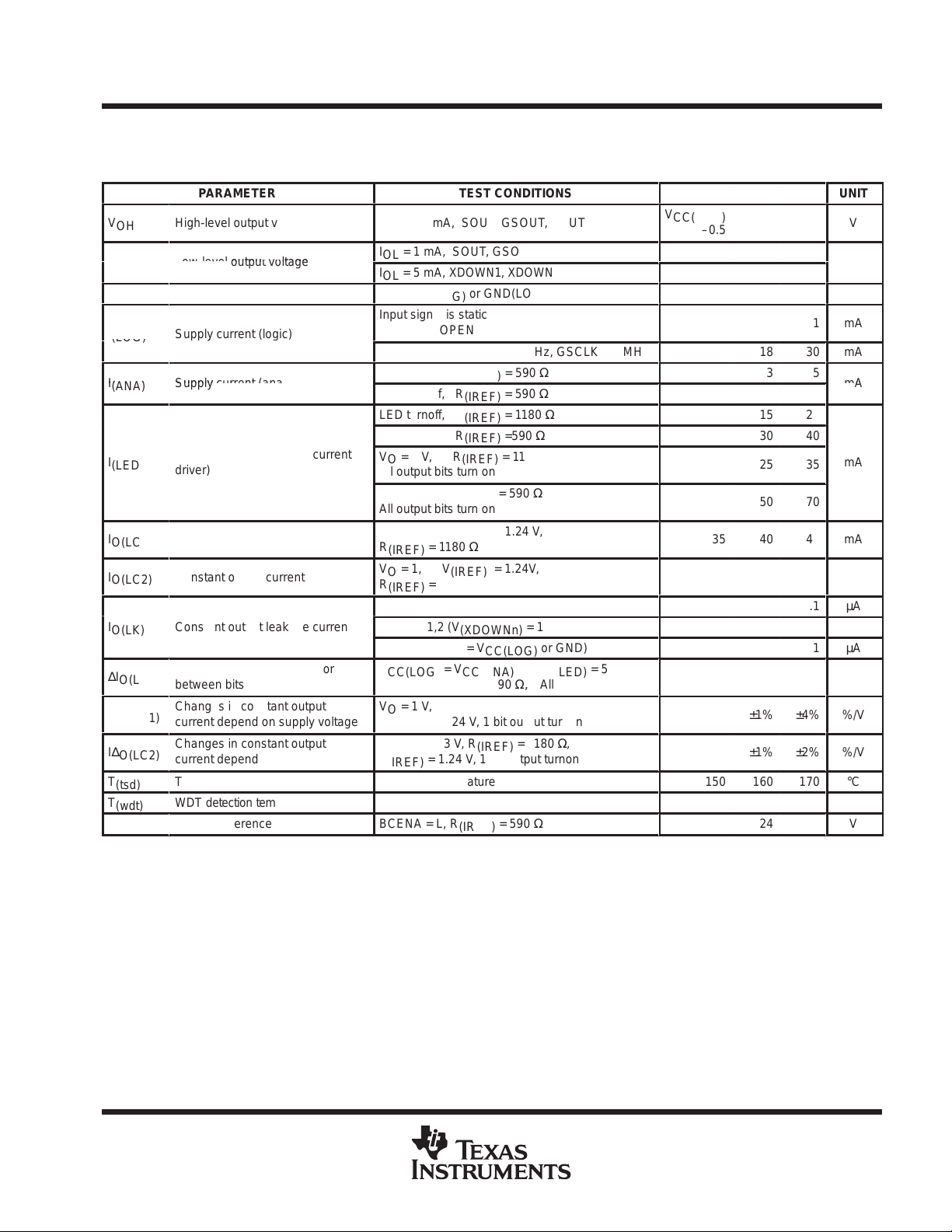
electrical characteristics,
= V
p
= V
CC(ANA)
CC(ANA)
MIN/MAX:V
TYP: V
V
I
I
I
I
I
I
∆I
I∆
I∆
T
T
V
OH
ÁÁ
I
ÁÁ
(ANA)
(LED)
ÁÁ
O(LC1)
ÁÁ
O(LC2)
O(LK)
O(LC)
ÁÁ
O(LC1)
O(LC2)
ÁÁ
(tsd)
(wdt)
(IREF)
CC(LOG)
High-level output voltage
Input current
Supply current (logic)
Supply current (constant current
driver)
Constant output current
Constant output current
Constant output leakage current
Constant output current error
between bits
Changes in constant output
current depend on supply voltage
Changes in constant output
current depend on output voltage
TSD detection temperature
WDT detection temperature
Voltage reference
CC(LOG)
PARAMETER
БББББББ
БББББББ
pp
БББББББ
БББББББ
БББББББ
БББББББ
= V
= V
= 4.5 V to 5.5 V, T
CC(LED)
CC(LED)
A
= 5 V, TA = 25°C (unless otherwise noted)
TEST CONDITIONS
IOH = –1 mA, SOUT, GSOUT, BOUT
БББББББББББ
IOL = 1 mA, SOUT, GSOUT, BOUT
IOL = 5 mA, XDOWN1, XDOWN2
VI = V
CC(LOG)
or GND(LOG)
Input signal is static, TSENA = H,
БББББББББББ
WDCAP = OPEN
Data transfer, SCLK = 15 MHz, GSCLK = 8 MHz
LED turnon, R
LED turnoff, R
LED turnoff, R
LED turnoff, R
VO = 1 V, R
All output bits turn on
БББББББББББ
VO = 1 V, R
All output bits turn on
VO = 1 V, V
БББББББББББ
R
(IREF)
VO = 1, V
R
(IREF)
(IREF)
= 1180 Ω
(IREF)
= 590 Ω
OUT0 to OUT15 (V
XDOWN1,2 (V
SOUT (V
V
VO = 1V , R
БББББББББББ
VO = 1 V, R
V
OUTn
CC(LOG)
= V
(IREF)
(IREF)
= 1.24 V, 1 bit output turnon
(IREF)
VO= 1 V to 3 V, R
БББББББББББ
V
= 1.24 V, 1 bit output turnon
(IREF)
= 590 Ω
(IREF)
= 590 Ω
(IREF)
= 1180 Ω
(IREF)
=590 Ω
(IREF)
= 1180 Ω
(IREF)
= 590 Ω
(IREF)
= 1.24 V,
= 1.24V,
= 15 V)
(OUTn)
(XDOWNn)
= V
CC(ANA)
= 15 V)
= V
or GND)
CC(LED)
CC(LOG)
= 590 Ω, All output bits turnon
= 1180 Ω,
= 1180 Ω,
(IREF)
Junction temperature
No external capacitor
BCENA = L, R
(IREF)
= 590 Ω
= –20 to 85°C
= 5 V,
LED DRIVER
SLLS401 – NOVEMBER 1999
MIN
V
CC(LOG)
ÁÁ
ÁÁÁÁÁÁ
ÁÁÁÁ
ÁÁ
ÁÁÁÁ
ÁÁÁÁ
TYP
–0.5
ÁÁÁÁÁ
18
3
3
15
30
25
50
35
70
Á
40
80
±1%
±1%
±1%
150
160
5
10
1.24
MAX
Á
Á
Á
Á
TLC5905
UNIT
0.5
0.5
±1
1
Á
30
5
5
20
40
35
Á
70
45
Á
90
0.1
1
1
±4%
Á
±4%
±2%
170
15
%/V
%/V
Á
V
µA
mA
mA
mA
mA
mA
µA
µA
µA
°C
ms
V
POST OFFICE BOX 655303 • DALLAS, TEXAS 75265
9
 Loading...