

Texas Instruments TLC32045EFN, TLC32045CN, TLC32045CFN, TLC32044MJB, TLC32044MJ Datasheet
...
TLC32044C, TLC32044E, TLC32044I, TLC32044M, TLC32045C, TLC32045I
VOICE-BAND ANALOG INTERFACE CIRCUITS
SLAS017F – MARCH 1988 – REVISED MA Y 1995
1
POST OFFICE BOX 655303 • DALLAS, TEXAS 75265
D
14-Bit Dynamic Range ADC and DAC
D
2’s Complement Format
D
Variable ADC and DAC Sampling Rate Up
to 19,200 Samples per Second
D
Switched-Capacitor Antialiasing Input Filter
and Output-Reconstruction Filter
D
Serial Port for Direct Interface to
TMS(SMJ)320C17, TMS(SMJ)32020,
TMS(SMJ)320C25,
and TMS320C30 Digital Signal Processors
D
Synchronous or Asynchronous ADC and
DAC Conversion Rates With Programmable
Incremental ADC and DAC Conversion
Timing Adjustments
D
Serial Port Interface to SN74(54)299
Serial-to-Parallel Shift Register for Parallel
Interface to TMS(SMJ)32010,
TMS(SMJ)320C15, or Other Digital
Processors
D
Internal Reference for Normal Operation
and External Purposes, or Can Be
Overridden by External Reference
D
CMOS Technology
description
The TLC32044 and TLC32045 are complete
analog-to-digital and digital-to-analog input and
output systems on single monolithic CMOS chips.
The TLC32044 and TLC32045 integrate a
bandpass switched-capacitor antialiasing input
filter, a 14-bit-resolution A/D converter, four
microprocessor-compatible serial port modes, a
14-bit-resolution D/A converter, and a low-pass
switched-capacitor output-reconstruction filter.
The devices offer numerous combinations of
master clock input frequencies and conversion/
sampling rates, which can be changed via digital
processor control.
Copyright 1995, Texas Instruments Incorporated
PRODUCTION DATA information is current as of publication date.
Products conform to specifications per the terms of Texas Instruments
standard warranty. Production processing does not necessarily include
testing of all parameters.
Please be aware that an important notice concerning availability, standard warranty, and use in critical applications of
Texas Instruments semiconductor products and disclaimers thereto appears at the end of this data sheet.
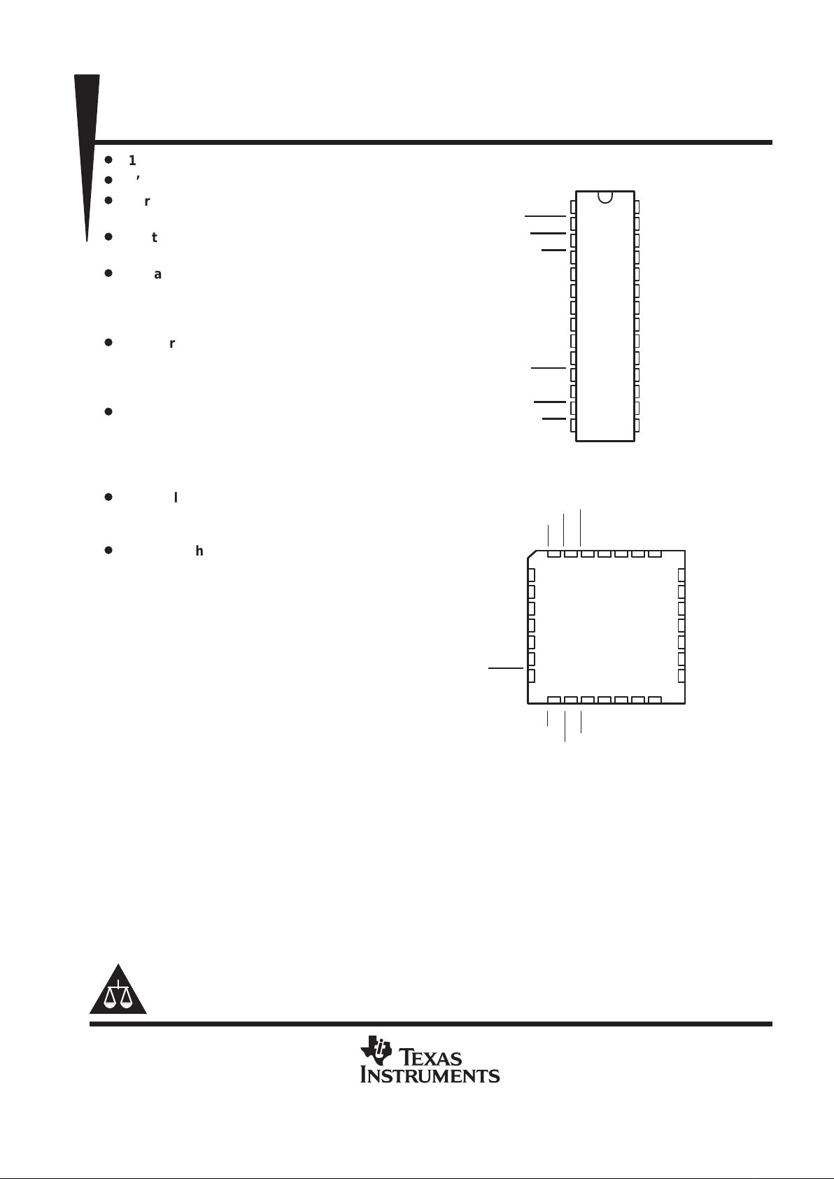
1
2
3
4
5
6
7
8
9
10
11
12
13
14
28
27
26
25
24
23
22
21
20
19
18
17
16
15
NU
RESET
EODR
FSR
DR
MSTR CLK
V
DD
REF
DGTL GND
SHIFT CLK
EODX
DX
WORD/BYTE
FSX
NU
NU
IN+
IN–
AUX IN+
AUX IN–
OUT+
OUT–
V
CC+
V
CC–
ANLG GND
ANLG GND
NU
NU
J† OR N PACKAGE
(TOP VIEW)
32 1
13 14
5
6
7
8
9
10
11
IN–
AUX IN+
AUX IN–
OUT+
OUT–
V
CC+
V
CC–
DR
MSTR CLK
V
DD
REF
DGTL GND
SHIFT CLK
EODX
4
15 16 17 18
WORD/BYTE
FSX
NU
NU
ANLG GND
ANLG GND
FSR
EODR
RESET
NU
28 27 26
25
24
23
22
21
20
19
12
DX
NU
IN +
NU
NU – Nonusable; no external connection should be made to
these terminals (see Table 2).
FK OR FN PACKAGE
(TOP VIEW)
†
Refer to the mechanical data for the JT package.
TLC32044C, TLC32044E, TLC32044I, TLC32044M, TLC32045C, TLC32045I
VOICE-BAND ANALOG INTERFACE CIRCUITS
SLAS017F – MARCH 1988 – REVISED MA Y 1995
2
POST OFFICE BOX 655303 • DALLAS, TEXAS 75265
AVAILABLE OPTIONS
PACKAGE
T
A
PLASTIC CHIP
CARRIER
(FN)
PLASTIC DIP
(N)
CERAMIC DIP
(J)
CHIP CARRIER
(FK)
°
°
TLC32044CFN TLC32044CN
0°C to 70°C
TLC32045CFN TLC32045CN
–20°C to 85°C TLC32044EFN
°
°
TLC32044IN
–
40°C to 85°C
TLC32045IN
–55°C to 125°C TLC32044MJ TLC32044MFK
description (continued)
Typical applications for the TLC32044 and TLC32045 include speech encryption for digital transmission,
speech recognition/ storage systems, speech synthesis, modems (7.2-, 8-, 9.6-, 14.4-, and 19.2-kHz sampling
rate), analog interface for digital signal processors (DSPs), industrial process control, biomedical
instrumentation, acoustical signal processing, spectral analysis, data acquisition, and instrumentation
recorders. Four serial modes, which allow direct interface to the TMS(SMJ)320C17, TMS(SMJ)32020,
TMS(SMJ)320C25, and TMS(SMJ)320C30 digital signal processors, are provided. Also, when the transmit and
receive sections of the analog interface circuit (AIC) are operating synchronously, it will interface to two
SN74(54)299 serial-to-parallel shift registers. These serial-to-parallel shift registers can then interface in
parallel to the TMS(SMJ)32010, TMS(SMJ)320C15, and other digital signal processors, or external FIFO
circuitry . Output data pulses are emitted to inform the processor that data transmission is complete or to allow
the DSP to differentiate between two transmitted bytes. A flexible control scheme is provided so that the
functions of the TLC32044 or TLC32045 can be selected and adjusted coincidentally with signal processing via
software control.
The antialiasing input filter comprises eighth-order and fourth-order CC-type (Chebyshev/elliptic transitional)
low-pass and high-pass filters, respectively. The input filter is implemented in switched-capacitor technology
and is preceded by a continuous time filter to eliminate any possibility of aliasing caused by sampled data
filtering. When only low-pass filtering is desired, the high-pass filter can be switched out of the signal path. A
selectable, auxiliary , dif ferential analog input is provided for applications where more than one analog input is
required.
The A/D and D/A architectures ensure no missing codes and monotonic operation. An internal voltage reference
is provided to ease the design task and to provide complete control over the performance of the TLC32044 or
TLC32045. The internal voltage reference is brought out to a terminal and is available to the designer. Separate
analog and digital voltage supplies and grounds are provided to minimize noise and ensure a wide dynamic
range. Also, the analog circuit path contains only differential circuitry to keep noise to an absolute minimum.
The only exception is the DAC sample and hold, which utilizes pseudo-differential circuitry.
The output-reconstruction filter is an eighth-order CC-type (Chebyshev/elliptic transitional low-pass filter)
followed by a second-order (sin x)/x correction filter and is implemented in switched-capacitor technology . This
filter is followed by a continuous-time filter to eliminate images of the digitally encoded signal. The on-board
(sin x)/x correction filter can be switched out of the signal path using digital signal processor control, if desired.
The TLC32044C and TLC32045C are characterized for operation from 0°C to 70°C. The TLC32044E is
characterized for operation from –20°C to 85°C. The TLC32044I and TLC32045I are characterized for
operation from –40°C to 85°C. The TLC32044M is characterized for operation from –55°C to 125°C.
TLC32044C, TLC32044E, TLC32044I, TLC32044M, TLC32045C, TLC32045I
VOICE-BAND ANALOG INTERFACE CIRCUITS
SLAS017F – MARCH 1988 – REVISED MA Y 1995
3
POST OFFICE BOX 655303 • DALLAS, TEXAS 75265
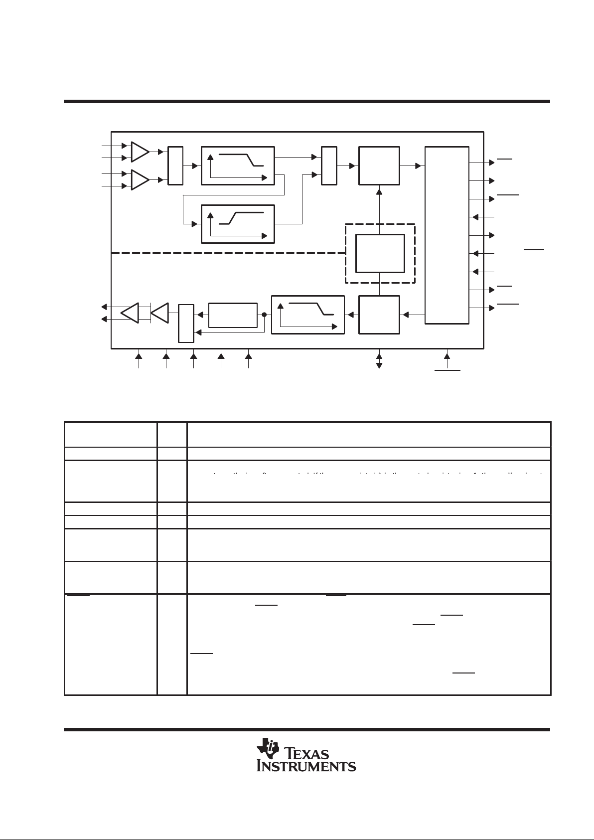
functional block diagram
M
U
X
M
U
X
IN+
IN–
AUX IN +
AUX IN –
Internal
Voltage
Reference
SHIFT CLK
MSTER CLK
EODR
DR
FSR
WORD/BYTE
DX
FSX
EODX
SERIAL
PORT
A/D
OUT+
OUT–
M
U
X
D/A
sin x/x
Correction
Filter
Filter
Transmit Section
V
CC+VCC–
ANLG
GND
DTGL
GND
V
DD
(Digital)
REF RESET
Receive Section
Terminal Functions
TERMINAL
NAME NO.
I/O
DESCRIPTION
ANLG GND 17,18 Analog ground return for all internal analog circuits. Not internally connected to DGTL GND.
AUX IN+ 24 I Noninverting auxiliary analog input stage. AUX IN + can be switched into the bandpass filter and A/D
converter path via software control. If the appropriate bit in the control register is a 1, the auxiliary inputs
p
–
p
–
p
will re lace the IN+ and IN– in uts. If the bit is a 0, the IN+ and IN– in uts will be used (see the AIC DX
data word format section).
AUX IN– 23 I Inverting auxiliary analog input (see the above AUX IN+ description).
DGTL GND 9 Digital ground for all internal logic circuits. Not internally connected to ANLG GND.
DR 5 O Data receive. DR is used to transmit the ADC output bits from the AIC to the TMS320 (SMJ320) serial port.
This transmission of bits from the AIC to the TMS320 (SMJ320) serial port is synchronized with the SHIFT
CLK signal.
DX 12 I Data transmit. DX is used to receive the DAC input bits and timing and control information from the TMS320
(SMJ320). This serial transmission from the TMS320 (SMJ320) serial port to the AIC is synchronized with
the SHIFT CLK signal.
EODR 3 O End of data receive. (See the WORD/BYTE description and Serial Port Timing diagram.) During the
word-mode timing, EODR
is a low-going pulse that occurs immediately after the 16 bits of A/D information
have been transmitted from the AIC to the TMS320 (SMJ320) serial port. EODR
can be used to interrupt
a microprocessor upon completion of serial communications. Also, EODR
can be used to strobe and enable
external serial-to-parallel shift registers, latches, or external FIFO RAM, and to facilitate parallel data bus
communications between the AIC and the serial-to-parallel shift registers. During the byte-mode timing,
EODR
goes low after the first byte has been transmitted from the AIC to the TMS320 (SMJ320) serial port
and is kept low until the second byte has been transmitted. The DSP can use this low-going signal to
differentiate between the two bytes as to which is first and which is second. EODR
does not occur after
secondary communication.
TLC32044C, TLC32044E, TLC32044I, TLC32044M, TLC32045C, TLC32045I
VOICE-BAND ANALOG INTERFACE CIRCUITS
SLAS017F – MARCH 1988 – REVISED MA Y 1995
4
POST OFFICE BOX 655303 • DALLAS, TEXAS 75265
Terminal Functions (continued)
TERMINAL
NAME NO.
I/O
DESCRIPTION
EODX
11 O End of data transmit. (See the WORD/BYTE description and Serial Port Timing diagram.) During the
word-mode timing, EODX
is a low-going pulse that occurs immediately after the 16 bits of D/A converter
and control or register information have been transmitted from the TMS320 (SMJ320) serial port to the AIC.
EODX
can be used to interrupt a microprocessor upon the completion of serial communications. Also,
EODX
can be used to strobe and enable external serial-to-parallel shift registers, latches, or an external
FIFO RAM, and to facilitate parallel data-bus communications between the AIC and the serial-to-parallel
shift registers. During the byte-mode timing, EODX
goes low after the first byte has been transmitted from
the TMS320 (SMJ320) serial port to the AIC and is kept low until the second byte has been transmitted. The
DSP can use this low-going signal to differentiate between the two bytes as to which is first and which is
second.
FSR
4 O Frame sync receive. In the serial transmission modes, which are described in the WORD/BYTE description,
FSR
is held low during bit transmission. When FSR goes low, the TMS320 (SMJ320) serial port begins
receiving bits from the AIC via DR of the AIC. The most significant DR bit is present on DR before FSR
goes
low. (See Serial Port Timing and Internal Timing Configuration diagrams.) FSR
does not occur after
secondary communications.
FSX
14 O Frame sync transmit. When FSX goes low , the TMS320 (SMJ320) serial port begins transmitting bits to the
FSX
yg,()gg
AIC via DX of the AIC. In all serial transmission modes, which are described in the WORD/BYTE description,
FSX is held low during bit transmission (see Serial Port Timing and Internal Timing Configuration diagrams).
IN+ 26 I Noninverting input to analog input amplifier stage
IN– 25 I Inverting input to analog input amplifier stage
MSTR CLK 6 I Master clock. MSTR CLK is used to derive all the key logic signals of the AIC, such as the shift clock, the
switched-capacitor filter clocks, and the A/D and D/A timing signals. The Internal Timing Configuration
diagram shows how these key signals are derived. The frequencies of these key signals are synchronous
submultiples of the master clock frequency to eliminate unwanted aliasing when the sampled analog signals
are transferred between the switched-capacitor filters and the A/D and D/A converters (see the Internal
Timing Configuration diagram).
OUT+ 22 O Noninverting output of analog output power amplifier. OUT+ can drive transformer hybrids or
high-impedance loads directly in either a differential or a single-ended configuration.
OUT– 21 O Inverting output of analog output power amplifier. OUT– is functionally identical with and complementary
to OUT+.
REF 8 I/O Internal voltage reference. An internal reference voltage is brought out on REF. An external voltage
reference can also be applied to REF.
RESET 2 I Reset function. RESET is provided to initialize the T A, T A’, TB, RA, RA’, RB, and control registers. A reset
initiates serial communications between the AIC and DSP. A reset initializes all AIC registers including the
control register. After a negative-going pulse on RESET
, the AIC registers are initialized to provide an 8-khz
data conversion rate for a 5.184-MHz master clock input signal. The conversion rate adjust registers, TA’
and RA’, are reset to 1. The control register bits are reset as follows (see AIC DX data word format section):
d9 = 1, d7 = 1, d6 = 1, d5 = 1, d4 = 0, d3 = 0, d2 = 1.
This initialization allows normal serial-port communication to occur between the AIC and DSP.
SHIFT CLK 10 O Shift clock. SHIFT CLK is obtained by dividing the master clock signal frequency by four. SHIFT CLK is used
to clock the serial data transfers of the AIC, described in the WORD/BYTE
description below (see the Serial
Port Timing and Internal Timing Configuration diagrams).
V
DD
7 Digital supply voltage, 5 V ±5%
V
CC+
20 Positive analog supply voltage, 5 V ±5%
V
CC–
19 Negative analog supply voltage, –5 V ±5%
TLC32044C, TLC32044E, TLC32044I, TLC32044M, TLC32045C, TLC32045I
VOICE-BAND ANALOG INTERFACE CIRCUITS
SLAS017F – MARCH 1988 – REVISED MA Y 1995
5
POST OFFICE BOX 655303 • DALLAS, TEXAS 75265
Terminal Functions (continued)
TERMINAL
NAME NO.
I/O
DESCRIPTION
WORD/BYTE 13 I Used in conjunction with a bit in the control register, WORD/BYTE is used to establish one of four serial
modes. These four serial modes are described below.
AIC transmit and receive sections are operated asynchronously.
The following description applies when the AIC is configured to have asynchronous transmit and receive
sections. If the appropriate data bit in the control register is a 0 (see the AIC DX data word format section),
the transmit and receive sections are asynchronous.
L Serial port directly interfaces with the serial port of the DSP and communicates in two
8-bit bytes. The operation sequence is as follows (see Serial Port Timing diagrams).
1. FSX
or FSR is brought low.
2. One 8-bit byte is transmitted or one 8-bit byte is received.
3. EODX
or EODR is brought low.
4. FSX
or FSR emits a positive frame-sync pulse that is four shift clock cycles wide.
5. One 8-bit byte is transmitted or one 8-bit byte is received.
6. EODX
or EODR is brought high.
7. FSX
or FSR is brought high.
H Serial port directly interfaces with the serial ports of the TMS(SMJ)32020, TMS(SMJ)320C25, or
TMS(SMJ)320C30, and communicates in one 16-bit word. The operation sequence is as follows
(see Serial Port Timing diagrams):
1. FSX
or FSR is brought low.
2. One 16-bit word is transmitted or one 16-bit word is received.
3. FSX
or FSR is brought high.
4. EODX
or EODR emits a low-going pulse.
AIC transmit and receive sections are operated synchronously.
If the appropriate data bit in the control register is 1, the transmit and receive sections are configured to be
synchronous. In this case, the bandpass switched-capacitor filter and the A/D conversion timing are derived
from the TX counter A, TX counter B, and TA, T A ’, and TB registers, rather than the RX counter A, RX counter
B, and RA, RA’, and RB registers. In this case, the AIC FSX
and FSR timing are identical during primary
data communication; however, FSR
is not asserted during secondary data communication since there is
no new A/D conversion result. The synchronous operation sequences are as follows (see Serial Port Timing
diagrams).
L Serial port directly interfaces with the serial port of the DSP and communicates in two 8-bit
bytes. The operation sequence is as follows (see Serial Port Timing diagrams):
1. FSX
and FSR are brought low.
2. One 8-bit byte is transmitted and one 8-bit byte is received.
3. EODX
and EODR are brought low.
4. FSX
and FSR emit positive frame-sync pulses that are four shift clock cycles wide.
5. One 8-bit byte is transmitted and one 8-bit byte is received.
6. EODX
and EODR are brought high.
7. FSX
and FSR are brought high.
H Serial port directly interfaces with the serial port of the TMS(SJM)32020, TMS(SMJ)320C25, or
TMS320C30, and communicates in one 16-bit word. The operation sequence is as follows (see
Serial Port Timing diagrams):
1. FSX
and FSR are brought low.
2. One 16-bit word is transmitted and one 16-bit word is received.
3. FSX
and FSR are brought high.
4. EODX
or EODR emit low-going pulses.
Since the transmit and receive sections of the AIC are now synchronous, the AIC serial port with additional
NOR and AND gates interface to two SN74(54)299 serial-to-parallel shift registers. Interfacing the AIC to
the SN74(54)299 shift register allows the AIC to interface to an external FIFO RAM and facilitates parallel,
data bus communications between the AIC and the digital signal processor. The operation sequence is the
same as the above sequence (see Serial Port Timing diagrams).

TLC32044C, TLC32044E, TLC32044I, TLC32044M, TLC32045C, TLC32045I
VOICE-BAND ANALOG INTERFACE CIRCUITS
SLAS017F – MARCH 1988 – REVISED MA Y 1995
6
POST OFFICE BOX 655303 • DALLAS, TEXAS 75265
PRINCIPLES OF OPERATION
analog input
Two sets of analog inputs are provided. Normally , the IN+ and IN– input set is used; however, the auxiliary input
set, AUX IN + and AUX IN–, can be used if a second input is required. Each input set can be operated in either
differential or single-ended modes, since sufficient common-mode range and rejection are provided. The gain
for the IN +, IN–, AUX IN +, and AUX IN– inputs can be programmed to be either 1, 2, or 4 (see T able 2). Either
input circuit can be selected via software control. It is important to note that a wide dynamic range is assured
by the differential internal analog architecture and by the separate analog and digital voltage supplies and
grounds.
A/D bandpass filter, A/D bandpass filter clocking, and A/D conversion timing
The A/D high-pass filter can be selected or bypassed via software control. The frequency response of this filter
is presented in the following pages. This response results when the switched-capacitor filter clock frequency
is 288 kHz and the A/D sample rate is 8 kHz. Several possible options can be used to attain a 288-kHz
switched-capacitor filter clock. When the filter clock frequency is not 288 kHz, the low-pass filter transfer function
is frequency scaled by the ratio of the actual clock frequency to 288 kHz. The ripple bandwidth and 3-dB
low-frequency roll-off points of the high-pass section are 150 Hz and 100 Hz, respectively. However, the
high-pass section low-frequency roll-off is frequency scaled by the ratio of the A/D sample rate to 8 kHz.
The internal timing configuration and AIC DX data word format sections of this data sheet indicate the many
options for attaining a 288-kHz bandpass switched-capacitor filter clock. These sections indicate that the RX
counter A can be programmed to give a 288-kHz bandpass switched-capacitor filter clock for several master
clock input frequencies.
The A/D conversion rate is then attained by frequency dividing the 288-kHz bandpass switched-capacitor filter
clock with the RX counter B. Unwanted aliasing is prevented because the A/D conversion rate is an integral
submultiple of the bandpass switched-capacitor filter sampling rate, and the two rates are synchronously
locked.
A/D converter performance specifications
Fundamental performance specifications for the A/D converter circuitry are presented in the A/D converter
operating characteristics section of this data sheet. The realization of the A/D converter circuitry with
switched-capacitor techniques provides an inherent sample-and-hold.
analog output
The analog output circuitry is an analog output power amplifier. Both noninverting and inverting amplifier outputs
are brought out. This amplifier can drive transformer hybrids or low-impedance loads directly in either a
differential or single-ended configuration.
D/A low-pass filter, D/A low-pass filter clocking, and D/A conversion timing
The frequency response of this filter is presented in the following pages. This response results when the
low-pass switched-capacitor filter clock frequency is 288 kHz. Like the A/D filter, the transfer function of this filter
is frequency scaled when the clock frequency is not 288 kHz. A continuous-time filter is provided on the output
of the (sin x)/x correction filter to eliminate the periodic sample data signal information, which occurs at multiples
of the 288-kHz switched-capacitor filter clock. The continuous time filter also greatly attenuates any
switched-capacitor clock feedthrough.

TLC32044C, TLC32044E, TLC32044I, TLC32044M, TLC32045C, TLC32045I
VOICE-BAND ANALOG INTERFACE CIRCUITS
SLAS017F – MARCH 1988 – REVISED MA Y 1995
7
POST OFFICE BOX 655303 • DALLAS, TEXAS 75265
PRINCIPLES OF OPERATION
D/A low-pass filter, D/A low-pass filter clocking, and D/A conversion timing (continued)
The D/A conversion rate is attained by frequency dividing the 288-kHz switched-capacitor filter clock with TX
Counter B. Unwanted aliasing is prevented because the D/A conversion rate is an integral submultiple of the
switched-capacitor low-pass filter sampling rate, and the two rates are synchronously locked.
asynchronous versus synchronous operation
If the transmit section of the AIC (low-pass filter and DAC) and receive section (bandpass filter and ADC) are
operated asynchronously , the low-pass and bandpass filter clocks are independently generated from the master
clock signal. Also, the D/A and A/D conversion rates are independently determined. If the transmit and receive
sections are operated synchronously, the low-pass filter clock drives both low-pass and bandpass filters. In
synchronous operation, the A/D conversion timing is derived from, and is equal to, the D/A conversion timing
(see description of the WORD/BYTE
in the Terminal Functions table.)
D/A converter performance specifications
Fundamental performance specifications for the D/A converter circuitry are presented in the D/A converter
operating characteristics section of the data sheet. The D/A converter has a sample-and-hold that is realized
with a switched-capacitor ladder.
system frequency response correction
The (sin x) /x correction for the D/A converter zero-order sample-and-hold output can be provided by an
on-board second-order (sin x)/x correction filter. This (sin x)/x correction filter can be inserted into or deleted
from the signal path by digital signal processor control. When inserted, the (sin x)/x correction filter follows the
switched-capacitor low-pass filter. When the TB register (see Internal T iming Configuration section) equals 36,
the correction results of Figures 11 and 12 can be obtained.
The (sin x)/x correction can also be accomplished by deleting the on-board second-order correction filter and
performing the (sin x)/x correction in digital signal processor software. The system frequency response can be
corrected via DSP software to ±0.1-dB accuracy to a band edge of 3000 Hz for all sampling rates. This correction
is accomplished with a first-order digital correction filter, which requires only seven TMS320 (SMJ320)
instruction cycles. With a 200-ns instruction cycle, seven instructions represent an overhead factor of only 1.1%
and 1.3% for sampling rates of 8 and 9.6 kHz, respectively (see the (sin x)/x correction section for more details).
serial port
The serial port has four possible modes that are described in detail in the Terminal Functions table. These
modes are briefly described below and in the functional description for WORD/BYTE
.
• The transmit and receive sections are operated asynchronously, and the serial port interfaces directly
with the DSP.
• The transmit and receive sections are operated asynchronously, and the serial port interfaces directly
with the TMS(SMJ)32020, TMS(SMJ)320C25, and the TMS(SMJ)320C30.
• The transmit and receive sections are operated synchronously, and the serial port interfaces directly
with the DSP.
• The transmit and receive sections are operated synchronously, and the serial port interfaces directly
with the TMS(SMJ)32020, TMS(SMJ)320C25, TMS(SMJ)320C30, or two SN74(54)299 serial-toparallel shift registers, which can then interface in parallel to the TMS(SMJ)32010, TMS(SMJ)320C15,
and SMJ320E15 to any other digital signal processor or to external FIFO circuitry.

TLC32044C, TLC32044E, TLC32044I, TLC32044M, TLC32045C, TLC32045I
VOICE-BAND ANALOG INTERFACE CIRCUITS
SLAS017F – MARCH 1988 – REVISED MA Y 1995
8
POST OFFICE BOX 655303 • DALLAS, TEXAS 75265
PRINCIPLES OF OPERATION
operation of TLC32044 or TLC32045 with internal voltage reference
The internal reference eliminates the need for an external voltage reference and provides overall circuit cost
reduction. Thus, the internal reference eases the design task and provides complete control over device
performance. The internal reference is brought out to a terminal and is available to the designer. To keep the
amount of noise on the reference signal to a minimum, an external capacitor can be connected between REF
and ANLG GND.
operation of TLC32044 or TLC32045 with external voltage reference
REF can be driven from an external reference circuit. This external circuit must be capable of supplying
250 µA and must be adequately protected from noise such as crosstalk from the analog input.
reset
A reset function is provided to initiate serial communications between the AIC and DSP and to allow fast,
cost-effective testing during manufacturing. The reset function initializes all AIC registers, including the control
register. After a negative-going pulse on RESET
, the AIC is initialized. This initialization allows normal serial port
communications activity to occur between AIC and DSP (see AIC DX data word format section).
loopback
This feature allows the user to test the circuit remotely . In loopback, OUT+ and OUT– are internally connected
to the IN+ and IN–. Thus, the DAC bits (d15 to d2), which are transmitted to DX, can be compared with the ADC
bits (d15 to d2), which are received from DR. An ideal comparison would be that the bits on DR equal the bits
on DX. However, there are some dif ference in these bits due to the ADC and DAC output offsets. The loopback
feature is implemented with digital signal processor control by transmitting the appropriate serial port bit to the
control register (see AIC DX data word format section).
TLC32044C, TLC32044E, TLC32044I, TLC32044M, TLC32045C, TLC32045I
VOICE-BAND ANALOG INTERFACE CIRCUITS
SLAS017F – MARCH 1988 – REVISED MA Y 1995
9
POST OFFICE BOX 655303 • DALLAS, TEXAS 75265
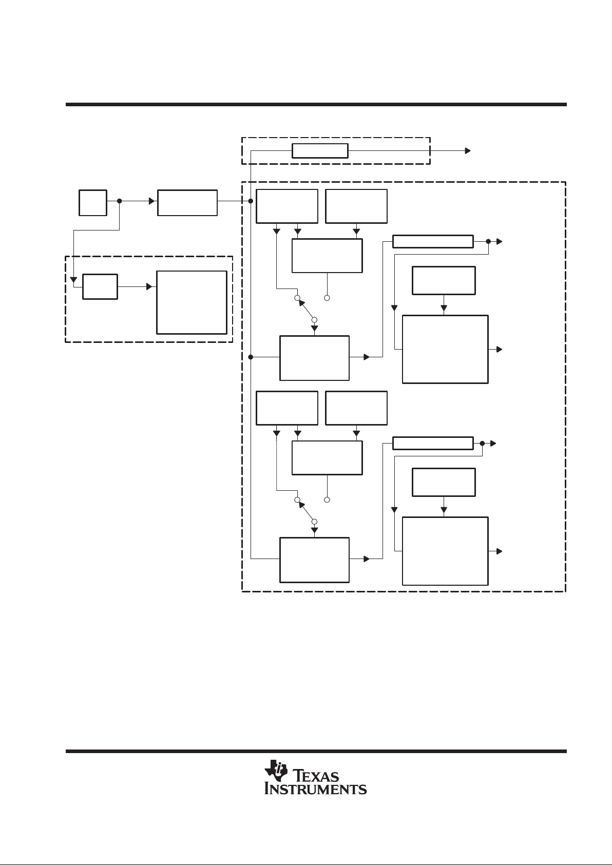
INTERNAL TIMING CONFIGURATION
XTAL
OSC
TMS(SMJ)320
DSP
Divide
by 135
Commercial
External
Front-End
Full-Duplex
Split-Band
Filters
†
TA Register
(5 bits)
TA’ Register
(6 bits)
(2’s compl)
Adder/
Subtractor
(6 bits)
Divide by 2
TB Register
(6 bits)
[TA = 9 (1)]
[TA = 18 (2)]
(6 bits)
TX Counter A
[TB = 40; 7.2 kHz]
[TB = 36; 8.0 kHz]
[TB = 30; 9.6 kHz]
[TB = 20; 14.4 kHz]
[TB = 15; 19.2 kHz]
TX Counter B
RA Register
(5 bits)
RA’ Register
(6 bits)
(2’s compl)
Adder/
Subtractor
(6 bits)
Divide by 2
RB Register
(6 bits)
[RA = 9 (1)]
[RA = 18 (2)]
(6 bits)
RX Counter A
[RB = 40; 7.2 kHz]
[RB = 36; 8.0 kHz]
[RB = 30; 9.6 kHz]
[RB = 20; 14.4 kHz]
[RB = 15; 19.2 kHz]
RX Counter B
Divide by 4
d0, d1 = 0,0
d0, d1 = 1,1
‡
d0, d1 = 0,1
d0, d1 = 1,0
‡
d0, d1 = 0,0
d0, d1 = 1,1
‡
d0, d1 = 0,1
d0, d1 = 1,0
‡
576-kHz
Pulses
576-kHz
Pulses
Low-Pass/
(sin x/x
Correction
Switched
Capacitor Filter
CLK = 288-kHz
Square Wave
D/A
Conversion
Frequency
A/D
Conversion
Frequency/
High-Pass
Switched
Capacitor
Filter CLK
Low-Pass
Switched
Capacitor Filter
CLK = 288-kHz
Square Wave
SHIFT CLK
1.296 MHz (1)
2.592 MHz (2)
MSTR CLK
5.184 MHz (1)
10.368 MHz (2)
20.736 MHz (1)
41.472 MHz (2)
Optional External Circuitry
for Full Duplex Modems
153.6-kHz
Clock (1)
†
Split-band filtering can alternatively be performed after the analog input function via software in the TMS(SMJ)320.
‡
These control bits are described in the AIC DX data word format section.
NOTE: Frequency 1 (20.736 MHz) is used to show how 153.6 kHz (for a commercially available modem split-band filter clock), popular speech
and modem sampling signal frequencies, and an internal 288-kHz switched-capacitor filter clock can be derived synchronously and as
submultiples of the crystal oscillator frequency . Since these derived frequencies are synchronous submultiples of the crystal frequency,
aliasing does not occur as the sampled analog signal passes between the analog converter and switched-capacitor filter stages.
Frequency 2 (41.472 MHz) is used to show that the AIC can work with high-frequency signals, which are used by high-speed digital signal
processors.
TLC32044C, TLC32044E, TLC32044I, TLC32044M, TLC32045C, TLC32045I
VOICE-BAND ANALOG INTERFACE CIRCUITS
SLAS017F – MARCH 1988 – REVISED MA Y 1995
10
POST OFFICE BOX 655303 • DALLAS, TEXAS 75265
explanation of internal timing configuration
All of the internal timing of the AIC is derived from the high-frequency clock signal that drives the master clock
input. The shift clock signal, which strobes the serial port data between the AIC and DSP, is derived by dividing
the master clock input signal frequency by four.
Low-pass:
SCF Clock Frequency (DńAorAńD path)
+
Master Clock Frequency
2 Contents of Counter A
Conversion Frequency
+
SCF Clock Frequency (DńAorAńD path)
Contents of Counter B
High-pass:
SCF Clock Frequency (AńD Path)+AńD Conversion Frequency
Shift Clock Frequency
+
Master Clock Frequency
4
TX counter A and TX counter B, which are driven by the master clock, determine the D/A conversion timing.
Similarly, RX counter A and RX counter B determine the A/D conversion timing. In order for the low-pass
switched-capacitor filter in the D/A path to meet its transfer function specifications, the frequency of its clock
input must be 288 kHz. If the clock frequency is not 288 kHz, the filter transfer function frequencies are
frequency-scaled by the ratios of the clock frequency to 288 kHz. Thus, to obtain the specified filter response,
the combination of master clock frequency and TX counter A and RX counter A values must yield a 288-kHz
switched-capacitor clock signal. This 288-kHz clock signal can then be divided by the TX counter B to establish
the D/A conversion timing.
The transfer function of the bandpass switched-capacitor filter in the A/D path is a composite of its high-pass
and low-pass section transfer functions. The high-frequency roll-off of the low-pass section meets the bandpass
filter transfer function specification when the low-pass section SCF is 288 kHz. Otherwise, the high-frequency
roll-off will be frequency-scaled by the ratio of the high-pass section’s SCF clock to 288 kHz. The low-frequency
roll-off of the high-pass section meets the bandpass filter transfer function specification when the A/D
conversion rate is 8 kHz. Otherwise, the low-frequency roll-off of the high-pass section is frequency-scaled by
the ratio of the A/D conversion rate to 8 kHz.
TX counter A and TX counter B are reloaded every D/A conversion period, while RX counter A and RX counter
B are reloaded every A/D conversion period. The TX counter B and RX counter B are loaded with the values
in the TB and RB registers, respectively . Via software control, the TX counter A can be loaded with either the
TA register, the TA register less the TA’ register, or the TA register plus the TA’ register. By selecting the TA
register less the TA’ register option, the upcoming conversion timing occurs earlier by an amount of time that
equals T A’ times the signal period of the master clock. By selecting the TA register plus the TA’ register option,
the upcoming conversion timing occurs later by an amount of time that equals T A ’ times the signal period of the
master clock. The D/A conversion timing can be advanced or retarded. An identical ability to alter the A/D
conversion timing is provided. In this case, however, the RX counter A can be programmed via software control
with the RA register, the RA register less the RA’ register, or the RA register plus the RA’ register.
The ability to advance or retard conversion timing is particularly useful for modem applications. This feature
allows controlled changes in the A/D and D/A conversion timing. This feature can be used to enhance
signal-to-noise performance, to perform frequency-tracking functions, and to generate nonstandard modem
frequencies.
TLC32044C, TLC32044E, TLC32044I, TLC32044M, TLC32045C, TLC32045I
VOICE-BAND ANALOG INTERFACE CIRCUITS
SLAS017F – MARCH 1988 – REVISED MA Y 1995
11
POST OFFICE BOX 655303 • DALLAS, TEXAS 75265
explanation of internal timing configuration (continued)
If the transmit and receive sections are configured to be synchronous (see WORD/BYTE description), then both
the low-pass and bandpass switched-capacitor filter clocks are derived from TX counter A. Also, both the D/A
and A/D conversion timing are derived from the TX counter A and TX counter B. When the transmit and receive
sections are configured to be synchronous, the RX counter A, RX counter B, RA register, RA’ register, and RB
registers are not used.
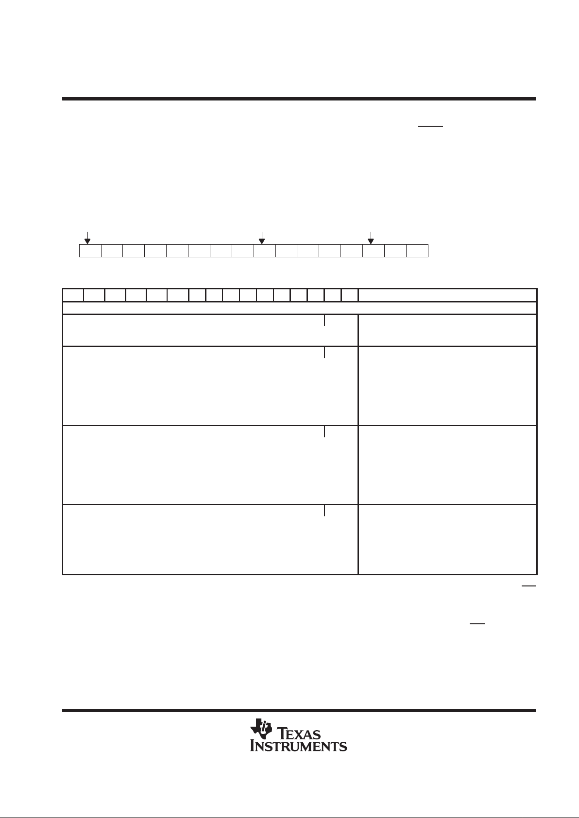
AIC DR or DX word bit pattern
d14 d13 d12 d11 d10 d9 d8 d7 d6 d5 d4 d3 d2 d1 d0d15
A/D or D/A MSB,
1st bit sent
1st bit sent of 2nd byte A/D or D/A LSB
AIC DX data word format section
d15 d14 d13 d12 d11 d10 d9 d8 d7 d6 d5 d4 d3 d2 d1 d0 Comments
primary DX serial communication protocol
←d15 (MSB) through d2 go to the D/A converter register → 0 0 The TX and RX counter As are loaded with the TA
and RA register values. The TX and RX counter Bs
are loaded with TB and RB register values.
←d15 (MSB) through d2 go to the D/A converter register → 0 1 The TX and RX counter As are loaded with the TA +
TA’ and RA + RA’ register values. The TX and RX
counter Bs are loaded with the TB and RB register
values. LSBs d1 = 0 and d0 =1 cause the next D/A
and A/D conversion periods to be changed by the
addition of T A ’ and RA ’ master clock cycles, in which
TA ’ and RA ’ can be positive or negative or zero (refer
to Table 1).
←d15 (MSB) through d2 go to the D/A converter register → 1 0 The TX and RX counter As are loaded with the T A –
TA’ and RA – RA’ register values. The TX and RX
counter Bs are loaded with the TB and RB register
values. LSBs d1 = 1 and d0 = 0 cause the next D/A
and A/D conversion periods to be changed by the
subtraction of TA’ and RA’ master clock cycles, in
which TA ’ and RA ’ can be positive or negative or zero
(refer to Table 1).
←d15 (MSB) through d2 go to the D/A converter register → 1 1 The TX and RX counter As are loaded with the TA
and RA register converter register values. The TX
and RX counter Bs are loaded with the TB and RB
register values. After a delay of four shift clock
cycles, a secondary transmission immediately
follows to program the AIC to operate in the desired
configuration.
NOTE: Setting the two least significant bits to 1 in the normal transmission of DAC information (primary communications) to the AIC initiates
secondary communications upon completion of the primary communications. Upon completion of the primary communication, FSX
remains high for four shift clock cycles and then goes low and initiates the secondary communication. The timing specifications for the
primary and secondary communications are identical. In this manner, the secondary communication, if initiated, is interleaved between
successive primary communications. This interleaving prevents the secondary communication from interfering with the primary
communications and DAC timing, thus preventing the AIC from skipping a DAC output. In the synchronous mode, FSR
is not asserted
during secondary communications.
TLC32044C, TLC32044E, TLC32044I, TLC32044M, TLC32045C, TLC32045I
VOICE-BAND ANALOG INTERFACE CIRCUITS
SLAS017F – MARCH 1988 – REVISED MA Y 1995
12
POST OFFICE BOX 655303 • DALLAS, TEXAS 75265
secondary DX serial communication protocol
x x | ← to TA register →| x x | ← to RA register → | 0 0 d13 and d6 are MSBs (unsigned binary)
x | ← to TA’ register →| x | ← to RA’ register → | 0 1 d14 and d7 are 2’s complement sign bits
x | ← to TB register → | x | ← to RB register → | 1 0 d14 and d7 are MSBs (unsigned binary)
x x x x x x d9 x d7 d6 d5 d4 d3 d2 1 1
Control
Register
d2 = 0/1 deletes/inserts the A/D high-pass filter
d3 = 0/1 disables/enables the loopback function
d4 = 0/1 disables/enables the AUX IN+ and AUX IN–
d5 = 0/1 asynchronous/synchronous transmit and receive sections
d6 = 0/1 gain control bits (see gain control section)
d7 = 0/1 gain control bits (see gain control section)
d9 = 0/1 delete/insert on-board second-order (sin x)/x correction filter
reset function
A reset function is provided to initiate serial communications between the AIC and DSP. The reset function
initializes all AIC registers, including the control register. After power has been applied to the AIC, a
negative-going pulse on RESET
initializes the AIC registers to provide an 8-kHz A/D and D/A conversion rate
for a 5.184 MHz master clock input signal. The AIC, except the control register, is initialized as follows (see AIC
DX data word format section):
REGISTER
INITIALIZED
REGISTER
VALUE (HEX)
TA 9
TA’ 1
TB 24
RA 9
RA’ 1
RB 24
The control register bits are reset as follows (see AIC DX data word format section):
d9 = 1, d7 = 1, d6 = 1, d5 = 1, d4 = 0, d3 = 0, d2 = 1
This initialization allows normal serial port communications to occur between AIC and DSP. If the transmit and
receive sections are configured to operate synchronously and the user wishes to program different conversion
rates, only the TA, TA’, and TB register need to be programmed, since both transmit and receive timing are
synchronously derived from these registers (see the terminal functions table and AIC DX word format sections).
The circuit shown in Figure 1 provides a reset on power up when power is applied in the sequence given under
power-up sequence. The circuit depends on the power supplies reaching their recommended values a minimum
of 800 ns before the capacitor charges to 0.8 V above DGTL GND.
V
CC+
V
CC–
RESET
200 kΩ
0.5 µF
TLC32044/TLC32045
5 V
–5 V
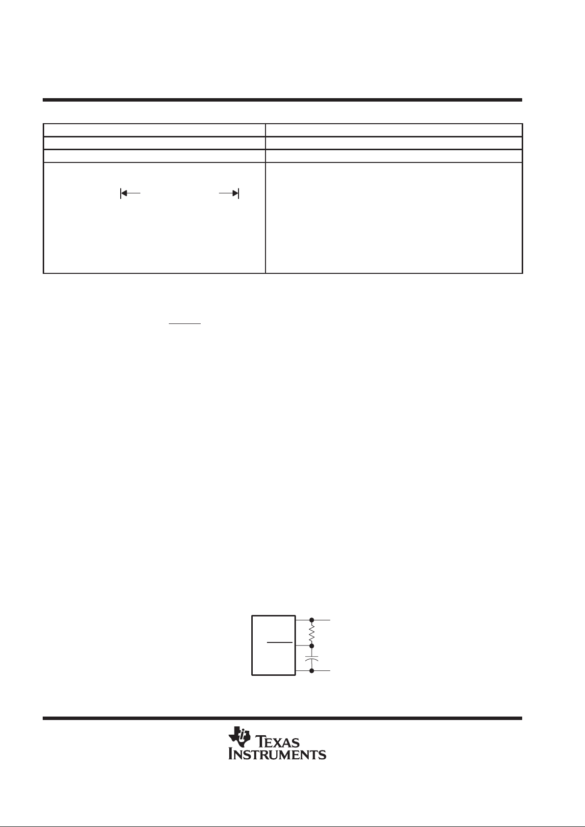
Figure 1. Power-Up Reset

TLC32044C, TLC32044E, TLC32044I, TLC32044M, TLC32045C, TLC32045I
VOICE-BAND ANALOG INTERFACE CIRCUITS
SLAS017F – MARCH 1988 – REVISED MA Y 1995
13
POST OFFICE BOX 655303 • DALLAS, TEXAS 75265
power-up sequence
To ensure proper operation of the AIC and as a safeguard against latch-up, it is recommended that Schottky
diodes with forward voltages less than or equal to 0.4 V be connected from V
CC–
to ANLG GND and from V
CC–
to DGTL GND (see Figure 21). In the absence of such diodes, power should be applied in the following
sequence: ANLG GND and DGTL GND, V
CC–
, then V
CC+
and VDD. Also, no input signal should be applied until
after power up.
AIC responses to improper conditions
The AIC has provisions for responding to improper conditions. These improper conditions and the response of
the AIC to these conditions are presented in Table 1 below.
AIC register constraints
The following constraints are placed on the contents of the AIC registers:
1. TA register must be ≥ 4 in word mode (WORD/BYTE
= high).
2. TA register must be ≥ 5 in byte mode (WORD/BYTE
= low).
3. TA’ register can be either positive, negative, or zero.
4. RA register must be ≥ 4 in word mode (WORD/BYTE
= high).
5. RA register must be ≥ 5 in byte mode (WORD/BYTE
= low).
6. RA’ register can be either positive, negative, or zero.
7. (TA register ± TA’ register) must be > 1.
8. (RA register ± RA’ register) must be > 1.
9. TB register must be > 1.
Table 1. AIC Responses to Improper Conditions
IMPROPER CONDITION AIC RESPONSE
TA register + TA’ register = 0 or 1
TA register – TA’ register = 0 or 1
Reprogram TX counter A with TA register value
TA register + TA’ register < 0 MODULO 64 arithmetic is used to ensure that a positive value is loaded into the TX counter A, i.e., T A
register + TA’ register + 40 hex is loaded into TX counter A.
RA register + RA’ register = 0 or 1
RA register – RA’ register = 0 or 1
Reprogram RX counter A with RA register value
RA register + RA’ register = 0 or 1 MODULO 64 arithmetic is used to ensure that a positive value is loaded into RX counter A, i.e., RA
register + RA’ register + 40 hex is loaded into RX counter A.
TA register = 0 or 1
RA register = 0 or 1
AIC is shut down.
TA register < 4 in word mode
TA register < 5 in byte mode
RA register < 4 in word mode
RA register < 5 in byte mode
The AIC serial port no longer operates.
TB register = 0 or 1 Reprogram TB register with 24 hex
RB register = 0 or 1 Reprogram RB register with 24 hex
AIC and DSP cannot communicate Hold last DAC output

TLC32044C, TLC32044E, TLC32044I, TLC32044M, TLC32045C, TLC32045I
VOICE-BAND ANALOG INTERFACE CIRCUITS
SLAS017F – MARCH 1988 – REVISED MA Y 1995
14
POST OFFICE BOX 655303 • DALLAS, TEXAS 75265
improper operation due to conversion times being too close together
If the difference between two successive D/A conversion frame syncs is less than 1/19.2 kHz, the AIC operates
improperly . In this situation, the second D/A conversion frame sync occurs too quickly and there is not enough
time for the ongoing conversion to be completed. This situation can occur if the A and B registers are improperly
programmed or if the A + A’ register or A – A’ register result is too small. When incrementally adjusting the
conversion period via the A + A ’ register options, the designer should be careful not to violate this requirement
(see following diagram).
Frame Sync FSX
or
FSR
t
1
t
2
Ongoing
Conversion
t2 – t1 1/19.2 kHz
asynchronous operation — more than one receive frame sync occurring between two transmit
frame syncs
When incrementally adjusting the conversion period via the A + A ’ or A – A ’ register options, a specific protocol
is followed. The command to use the incremental conversion period adjust option is sent to the AIC during a
FSX
frame sync. The ongoing conversion period is then adjusted. However, either receive conversion period
A or B can be adjusted. For both transmit and receive conversion periods, the incremental conversion period
adjustment is performed near the end of the conversion period. Therefore, if there is sufficient time between
t
1
and t2, the receive conversion period adjustment is performed during receive conversion period A. Otherwise,
the adjustment is performed during receive conversion period B. The adjustment command only adjusts one
transmit conversion period and one receive conversion period. To adjust another pair of transmit and receive
conversion periods, another command must be issued during a subsequent FSX
frame (see figure below).
t
1
t
2
Transmit Conversion Period
Receive Conv.
Period A
Receive Conv.
Period B
FSX
FSR
Figure 2. Adjusted Transmit and Receive Conversion Periods
asynchronous operation — more than one transmit frame sync occurring between two receive
frame syncs
When incrementally adjusting the conversion period via the A + A ’ or A – A ’ register options, a specific protocol
is followed. For both transmit and receive conversion periods, the incremental conversion period adjustment
is performed near the end of the conversion period. The command to use the incremental conversion period
adjust options is sent to the AIC during a FSX
frame sync. The ongoing transmit conversion period is then
adjusted. However, three possibilities exist for the receive conversion period adjustment in the diagram as
shown in the following figure. If the adjustment command is issued during transmit conversion period A, receive
conversion period A is adjusted if there is sufficient time between t
1
and t2. If there is not sufficient time between
t
1
and t2, receive conversion period B is adjusted. The receive portion of an adjustment command can be

TLC32044C, TLC32044E, TLC32044I, TLC32044M, TLC32045C, TLC32045I
VOICE-BAND ANALOG INTERFACE CIRCUITS
SLAS017F – MARCH 1988 – REVISED MA Y 1995
15
POST OFFICE BOX 655303 • DALLAS, TEXAS 75265
ignored if the adjustment command is sent during a receive conversion period, which is already being or will
be adjusted due to a prior adjustment command. For example, if adjustment commands are issued during
transmit conversion periods A, B, and C, the first two commands can cause receive conversion periods A and
B to be adjusted, while the third receive adjustment command is ignored. The third adjustment command is
ignored since it was issued during receive conversion period B, which already is adjusted via the transmit
conversion period B adjustment command.
Transmit
Conversion
Period A
Receive Conversion Period A
FSX
FSR
Transmit
Conversion
Period B
Transmit
Conversion
Period C
t
1
t
2
Receive Conversion Period B
Figure 3. Receive and Transmit Conversion Period Adjustments
asynchronous operation — more than one set of primary and secondary DX serial communication
occurring between two receive frame sync (see AIC DX data word format section)
The T A, T A ’, TB, and control register information that is transmitted in the secondary communications is always
accepted and is applied during the ongoing transmit conversion period. If there is sufficient time between t
1
and
t
2
, the TA, RA’, and RB register information, which is sent during transmit conversion period A, is applied to
receive conversion period A. Otherwise, this information is applied during receive conversion period B. If RA,
RA ’, and RB register information has already been received and is being applied during an ongoing conversion
period, any subsequent RA, RA’, or RB information that is received during this receive conversion period is
disregarded (see Figure 4).
FSX
FSR
Transmit
Conversion
Period A
Transmit
Conversion
Period B
Transmit
Conversion
Period C
t
1
t
2
Primary Secondary Primary Secondary Primary Secondary
Receive Conversion
Period A
Receive Conversion Period B
Figure 4. Receive and Transmit Periods for Primary and Secondary Data

TLC32044C, TLC32044E, TLC32044I, TLC32044M, TLC32045C, TLC32045I
VOICE-BAND ANALOG INTERFACE CIRCUITS
SLAS017F – MARCH 1988 – REVISED MA Y 1995
16
POST OFFICE BOX 655303 • DALLAS, TEXAS 75265
test modes
†
The TLC32044 or TLC32045 can be operated in special test modes. These test modes are used by Texas
Instruments to facilitate testing of the device during manufacturing. They are not intended to be used in real
applications; however, they allow the filters in the A/D and D/A paths to be used without using the A/D and D/A
converters.
In normal operation, the nonusable (NU) terminals are left unconnected. These NU terminals are used by the
factory to speed up testing of the TLC32044 or TLC32045 analog interface circuits (AIC). When the device is
used in normal (non-test mode) operation, the NU terminal (terminal 1) has an internal pulldown to – 5 V.
Externally connecting 0 V or 5 V to terminal 1 puts the device in test-mode operation. Selecting one of the
possible test modes is accomplished by placing a particular voltage on certain terminals. A description of these
modes is provided in Table 2 and Figures 5 and 6.
Table 2. List of Test Modes
TEST
D/A PATH TEST (TERMINAL 1 to 5 V) A/D PATH TEST (TERMINAL 1 to 0)
TERMINALS
TEST FUNCTION TEST FUNCTION
5 The low-pass switched-capacitor filter clock is brought out to The bandpass switched-capacitor filter clock is brought out to
g
DR. This clock signal is normally internal.
g
DR. This clock signal is normally internal.
11 No change from normal operation. The EODX signal is
brought out to EODX
.
The pulse that initiates the A/D conversion is brought out here.
This signal is normally internal.
3 The pulse that initiates the D/A conversion is brought out here. No change from normal operation. The EODR signal is
brought out.
27 and 28 There are no test output signals provided on these terminals. The outputs of the A/D path low-pass or bandpass filter
(depending upon control bit d2 – see AIC DX data word format
section) are brought out to these terminals. If the high-pass
section is inserted, the output will have a (sin x)/x droop. The
slope of the droop is determined by the ADC sampling
frequency, which is the high-pass section clock frequency
(see diagram of bandpass or low-pass filter test for receive
section). These outputs drive small (30-pF) loads.
15 and 16
D/A PATH LOW-PASS FILTER TEST: (WORD/BYTE) to –5 V
TEST FUNCTION
The inputs of the D/A path low-pass filter are brought out to terminals 15 and 16. The D/A input to this filter is removed. If (sin x)/x
correction filter is inserted, the OUT+ and OUT– signals have a flat response (see Figure 2). The common-mode range of these
inputs must not exceed ±0.5 V.
†
In the test mode, the AIC responds to the setting of WORD/BYTE to –5 V , as if WORD/BYTE were set to 0 V. Thus, the byte mode is selected
for communicating between DSP and AIC. Either of the path tests (D/A or A/D) can be performed simultaneously with the D/A low-pass filter test.
In this situation, WORD/BYTE
must be connected to –5 V , which initiates byte-mode communications.

TLC32044C, TLC32044E, TLC32044I, TLC32044M, TLC32045C, TLC32045I
VOICE-BAND ANALOG INTERFACE CIRCUITS
SLAS017F – MARCH 1988 – REVISED MA Y 1995
17
POST OFFICE BOX 655303 • DALLAS, TEXAS 75265
M
U
X
A/D
Filter
Test
Test Control
(terminal 1 at 0 V)
Terminal 27 (positive)
Terminal 28 (negative)
†
†
All analog signal paths have differential architecture and hence have positive and negative
components.
Figure 5. Bandpass or Low-Pass Filter Test for Receiver Section
Test
M
U
X
D/A
(sin x)/x
Correction
Filter
M
U
X
Test Control
(terminal 13 at –5 V)
Terminal 16 (positive)
Terminal 15 (negative)
†
†
All analog signal paths have differential architecture and hence have positive and negative components.
Figure 6. Low-Pass Filter Test for Transmit Section

TLC32044C, TLC32044E, TLC32044I, TLC32044M, TLC32045C, TLC32045I
VOICE-BAND ANALOG INTERFACE CIRCUITS
SLAS017F – MARCH 1988 – REVISED MA Y 1995
18
POST OFFICE BOX 655303 • DALLAS, TEXAS 75265
absolute maximum ratings over operating free-air temperature range (unless otherwise noted)
†
Supply voltage range, V
CC+
(see Note 1) –0.3 V to 15 V. . . . . . . . . . . . . . . . . . . . . . . . . . . . . . . . . . . . . . . . . . . .
Supply voltage range, V
DD
–0.3 V to 15 V. . . . . . . . . . . . . . . . . . . . . . . . . . . . . . . . . . . . . . . . . . . . . . . . . . . . . . . . .
Output voltage range, V
O
–0.3 V to 15 V. . . . . . . . . . . . . . . . . . . . . . . . . . . . . . . . . . . . . . . . . . . . . . . . . . . . . . . . . .
Input voltage range, V
I
–0.3 V to 15 V. . . . . . . . . . . . . . . . . . . . . . . . . . . . . . . . . . . . . . . . . . . . . . . . . . . . . . . . . . . . .
Digital ground voltage range –0.3 V to 15 V. . . . . . . . . . . . . . . . . . . . . . . . . . . . . . . . . . . . . . . . . . . . . . . . . . . . . . . .
Operating free-air temperature range: TLC32044C, TLC32045C 0°C to 70°C. . . . . . . . . . . . . . . . . . . . . . . . .
TLC32044E –20°C to 85°C. . . . . . . . . . . . . . . . . . . . . . . . . . . . . . . . . . .
TLC32044I, TLC32045I –40°C to 85°C. . . . . . . . . . . . . . . . . . . . . . . . .
TLC32044M –55°C to 125°C. . . . . . . . . . . . . . . . . . . . . . . . . . . . . . . . . .
Storage temperature range: TLC32044C, I, TLC32045C, I –40°C to 125°C. . . . . . . . . . . . . . . . . . . . . . . . . . .
TLC32044M –65°C to 150°C. . . . . . . . . . . . . . . . . . . . . . . . . . . . . . . . . . . . . . . . . .
Case temperature for 10 seconds: FN or FK package 260°C. . . . . . . . . . . . . . . . . . . . . . . . . . . . . . . . . . . . . . . . .
Lead temperature 1,6 mm (1/16 inch) from case for 10 seconds: N package 260°C. . . . . . . . . . . . . . . . . . . .
J package 300°C. . . . . . . . . . . . . . . . . . . .
†
Stresses beyond those listed under “absolute maximum ratings” may cause permanent damage to the device. These are stress ratings only, and
functional operation of the device at these or any other conditions beyond those indicated under “recommended operating conditions” is not
implied. Exposure to absolute-maximum-rated conditions for extended periods may affect device reliability.
NOTE 1: Voltage values for maximum ratings are with respect to V
CC–
.
recommended operating conditions
MIN NOM MAX UNIT
Supply voltage, V
CC+
(see Note 2) 4.75 5 5.25 V
Supply voltage, V
CC–
(see Note 2) –4.75 –5 –5.25 V
Digital supply voltage, VDD (see Note 2) 4.75 5 5.25 V
Digital ground voltage with respect to ANLG GND, DGTL GND 0 V
Reference input voltage, V
ref(ext)
(see Note 2) 2 4 V
High-level input voltage, V
IH
2 VDD+0.3 V
Low-level input voltage, VIL (see Note 3) –0.3 0.8 V
Load resistance at OUT+ and/or OUT–, R
L
300 Ω
Load capacitance at OUT+ and/or OUT–, C
L
100 pF
MSTR CLK frequency (see Note 4) 0.075 5 10.368 MHz
Analog input amplifier common mode input voltage (see Note 5) ±1.5 V
A/D or D/A conversion rate 20 kHz
TLC32044C, TLC32045C 0 70
p
p
TLC32044E –20 85
°
Operating free-air temperature, T
A
TLC32044I, TLC32045I –40 85
°C
TLC32044M –55 125
NOTES: 2. Voltages at analog inputs and outputs, REF , V
CC+
, and V
CC–,
are with respect to the ANLG GND terminal. Voltages at digital inputs
and outputs and VDD are with respect to the DGTL GND terminal.
3. The algebraic convention, in which the least positive (most negative) value is designated minimum, is used in this data sheet for
logic voltage levels and temperature only.
4. The bandpass switched-capacitor filter (SCF) specifications apply only when the low-pass section SCF clock is 288 kHz and the
high-pass section SCF clock is 8 kHz. If the low-pass SCF clock is shifted from 288 kHz, the low-pass roll-off frequency will shift
by the ratio of the low-pass SCF clock to 288 kHz. If the high-pass SCF is shifted from 8 kHZ, the high-pass roll-off frequency will
shift by the ratio of the high-pass SCF clock to 8 kHz. Similarly, the low-pass switched-capacitor filter (SCF) specifications apply only
when the SCF clock is 288 kHz. If the SCF clock is shifted from 288 kHz, the low-pass roll-off frequency will shift by the ratio of the
SCF clock to 288 kHz.
5. This range applies when (IN+ – IN–) or (AUX IN+ – AUX IN–) equals ± 6 V.
TLC32044C, TLC32044E, TLC32044I, TLC32044M, TLC32045C, TLC32045I
VOICE-BAND ANALOG INTERFACE CIRCUITS
SLAS017F – MARCH 1988 – REVISED MA Y 1995
19
POST OFFICE BOX 655303 • DALLAS, TEXAS 75265
electrical characteristics over recommended operating free-air temperature range, V
CC +
= 5 V,
V
CC –
= –5 V, VDD = 5 V (unless otherwise noted)
total device, MSTR CLK frequency = 5.184 MHz, outputs not loaded
PARAMETER TEST CONDITIONS MIN
TYP
†
MAX UNIT
V
OH
High-level output voltage
VDD = 4.75 V ,
IOH = –300 µA
2.4
V
OL
Low-level output voltage
VDD = 4.75 V ,
IOL = 2 mA
0.4
V
TLC32044C, TLC32045C 35
I
CC+
Supply current from V
CC+
TLC32044I, TLC32045I,
TLC32044E, TLC32044M
40
TLC32044C, TLC32045C –35
I
CC–
Supply current from V
CC–
TLC32044I, TLC32045I,
TLC32044E, TLC32044M
–40
mA
pp
TLC3204xC, E, I
7
IDDSupply current from V
DD
TLC32044M
f
MSTR CLK
=
5.184 MH
z
8
p
TLC3204xC, E, I 3 3.3
V
ref
Internal reference output voltage
TLC32044M 2.9 3.3
V
∝
Vref
Temperature coefficient of internal reference voltage 200 ppm/°C
r
o
Output resistance at REF 100 kΩ
receive amplifier input
PARAMETER TEST CONDITIONS MIN
TYP
†
MAX UNIT
TLC32044C, E, I 10 70
A/D converter offset error (filters in)
TLC32044M 10 85
mV
TLC32045C, I 10 75
Common-mode rejection ratio at IN+, IN–, or
TLC3204xC, E, I
55
CMRR
j,,
AUX IN+, AUX IN–
TLC32044M
See Note 6
35 55
dB
r
i
Input resistance at IN+, IN–, or AUX IN+, AUX IN–, REF 100 kΩ
transmit filter output
PARAMETER TEST CONDITIONS MIN
TYP
†
MAX UNIT
Output offset voltage at OUT+ OUT–
TLC3204xC, E, I 15 80
V
OO
g
(single-ended relative to ANLG GND)
TLC32044M
15 75
mV
V
OM
Maximum peak output voltage swing across RL at OUT+ or OUT–
(single ended)
RL ≥ 300 Ω,
Offset voltage = 0
±3
V
OM
Maximum peak output voltage swing between OUT+ and OUT–
(differential output)
RL ≥ 600 Ω ±6
V
†
All typical values are at TA = 25°C.
NOTE 6: The test condition is a 0-dBm, 1-kHz input signal with an 8-kHz conversion rate.
TLC32044C, TLC32044E, TLC32044I, TLC32044M, TLC32045C, TLC32045I
VOICE-BAND ANALOG INTERFACE CIRCUITS
SLAS017F – MARCH 1988 – REVISED MA Y 1995
20
POST OFFICE BOX 655303 • DALLAS, TEXAS 75265
system distortion specifications, SCF clock frequency = 288 kHz (see Note 7)
PARAMETER TEST CONDITIONS MIN
TYP
†
MAX UNIT
TLC3204xC, E, I
V
= –0.5 dB to –24 dB referred to V
,
70
Attenuation of second
p
Single ended
TLC32044M
Iref
,
TA = 25°C
62 70
harmonic of A/D input
signal
TLC32044C, E, I
62 70
signal
Differential
TLC32045C, I
V
I
= –
0.5 dB to –24 dB referred to V
ref
55 70
TLC3204xC, E, I
V
= –0.5 dB to –24 dB referred to V
,
65
Attenuation of third and
Single ended
TLC32044M
Iref
,
TA = 25°C
57 65
higher harmonics of A/D
input signal
TLC32044C, E, I
57 65
in ut signal
Differential
TLC32045C, I
V
I
= –0.5 dB to –24 dB
referred to V
ref
55 65
dB
Attenuation of second
Single ended TLC3204xC, I, M 70
Attenuation of second
harmonic of D/A input
TLC32044C, E, I
VI = –0 dB to –24 dB referred to V
ref
62 70
signal
Differential
TLC32045C, I 55 70
Attenuation of third and
Single ended TLC3204xC, I, M 65
Attenuation of third and
higher harmonics of D/A
TLC32044C, E, I
VI = –0 dB to –24 dB referred to V
ref
57 65
input signal
Differential
TLC32045C, I 55 65
†
All typical values are at TA = 25°C.
NOTE 7: The test condition VI is a 1-kHz input signal with an 8-kHz conversion rate (0 dB relative to V
ref
). The load impedance for the DAC is
600 Ω (300 Ω for TLC32044M).

TLC32044C, TLC32044E, TLC32044I, TLC32044M, TLC32045C, TLC32045I
VOICE-BAND ANALOG INTERFACE CIRCUITS
SLAS017F – MARCH 1988 – REVISED MA Y 1995
21
POST OFFICE BOX 655303 • DALLAS, TEXAS 75265
A/D channel signal-to-distortion ratio (see Note 7)
Av = 1
†
Av = 2
†
Av = 4
†
PARAMETER
TEST CONDITIONS
MIN MAX MIN MAX MIN MAX
UNIT
VI = –6 dB to –0.1 dB 58 >58
‡
>58
‡
VI = –12 dB to –6 dB 58 58 >58
‡
VI = –18 dB to –12 dB 56 58 58
VI = –24 dB to –18 dB 50 56 58
A/D channel signal-to-distortion ratio, TLC32044C,
VI = –30 dB to –24 dB 44 50 56
TLC32044I, TLC32044E
VI = –36 dB to –30 dB 38 44 50
VI = –42 dB to –36 dB 32 38 44
VI = –48 dB to –42 dB 26 32 38
VI = –54 dB to –48 dB 20 26 32
VI = –6 dB to –0.5 dB 58 >58
‡
>58
‡
VI = –12 dB to –6 dB 58 58 >58
‡
VI = –18 dB to –12 dB 56 58 58
VI = –24 dB to –18 dB 50 56 58
A/D channel signal-to-distortion ratio, TLC32044M
VI = –30 dB to –24 dB 44 50 56
dB
VI = –36 dB to –30 dB 38 44 50
VI = –42 dB to –36 dB 32 38 44
VI = –48 dB to –42 dB 26 32 38
VI = –54 dB to –48 dB 20 26 32
VI = –6 dB to –0.1 dB 55 >55
‡
>55
‡
VI = –12 dB to –6 dB 55 55 >55
‡
VI = –18 dB to –12 dB 53 55 55
VI = –24 dB to –18 dB 47 53 55
A/D ch
annel signal-to-distortion ratio,
TLC32045C
,
VI = –30 dB to –24 dB 41 47 53
TLC32045I
VI = –36 dB to –30 dB 35 41 47
VI = –42 dB to –36 dB 29 35 41
VI = –48 dB to –42 dB 23 29 35
VI = –54 dB to –48 dB 17 23 29
†
Av is the programmable gain of the input amplifier.
‡
A value >60 is over range and signal clipping occurs.
NOTE 7: The test condition VI is a 1-kHz input signal with an 8-kHz conversion rate (0 dB relative to V
ref
). The load impedance for the DAC is
600 Ω (300 Ω for TLC32044M).

TLC32044C, TLC32044E, TLC32044I, TLC32044M, TLC32045C, TLC32045I
VOICE-BAND ANALOG INTERFACE CIRCUITS
SLAS017F – MARCH 1988 – REVISED MA Y 1995
22
POST OFFICE BOX 655303 • DALLAS, TEXAS 75265
D/A channel signal-to-distortion ratio (see Note 7)
PARAMETER
TEST CONDITIONS
MIN
MAX
UNIT
VI = –6 dB to 0 dB 58
VI = –12 dB to –6 dB 58
VI = –18 dB to –12 dB 56
VI = –24 dB to –18 dB 50
D/A channel signal-to-distortion ratio, TLC32044C, TLC32044E, TLC32044I,
VI = –30 dB to –24 dB 44
TLC32044M
VI = –36 dB to –30 dB 38
VI = –42 dB to –36 dB 32
VI = –48 dB to –42 dB 26
VI = –54 dB to –48 dB 20
VI = –6 dB to 0 dB 55
dB
VI = –12 dB to –6 dB 55
VI = –18 dB to –12 dB 53
VI = –24 dB to –18 dB 47
D/A channel signal-to-distortion ratio, TLC32045C, TLC32045I
VI = –30 dB to –24 dB 41
VI = –36 dB to –30 dB 35
VI = –42 dB to –36 dB 29
VI = –48 dB to –42 dB 23
VI = –54 dB to –48 dB 17
NOTE 7: The test condition VI is a 1-kHz input signal with an 8-kHz conversion rate (0 dB relative to V
ref
). The load impedance for the DAC is
600 Ω (300 Ω for TLC32044M).
gain and dynamic range
PARAMETER TEST CONDITIONS MIN
TYP
†
MAX UNIT
Absolute transmit gain tracking error while transmitting
into 600 Ω
–48-dB to 0-dB signal range, See Note 8 ±0.05 ±0.15 dB
Absolute transmit gain tracking error while transmitting
into 300 Ω, TLC32044M
–48-dB to 0-dB signal range,
See Note 8
TA = 25°C,
±0.05 ±0.25 dB
Absolute transmit gain tracking error while transmitting
into 300 Ω, TLC32044M
–48-dB to 0-dB signal range,
TA = –55°C to 125°C, See Note 8
±0.4 dB
Absolute receive gain tracking error –48-dB to 0-dB signal range, See Note 8 ±0.05 ±0.15 dB
Absolute receive gain tracking error, TLC32044M
–48-dB to 0-dB signal range,
See Note 8
TA = 25°C,
±0.05 ±0.25 dB
Absolute receive gain tracking error, TLC32044M
–48-dB to 0-dB signal range,
TA = –55°C to 125°C, See Note 8
±0.4 dB
Absolute gain of the A/D channel Signal input is a –0.5-dB, 1-kHz sinewave 0.2
Absolute gain of the D/A channel Signal input is a 0-dB, 1-kHz sinewave –0.3
dB
†
All typical values are at TA = 25°C.
NOTE 8: Gain tracking is relative to the absolute gain at 1 kHz and 0 dB (0 dB relative to V
ref
).

TLC32044C, TLC32044E, TLC32044I, TLC32044M, TLC32045C, TLC32045I
VOICE-BAND ANALOG INTERFACE CIRCUITS
SLAS017F – MARCH 1988 – REVISED MA Y 1995
23
POST OFFICE BOX 655303 • DALLAS, TEXAS 75265
power supply rejection and crosstalk attenuation
PARAMETER TEST CONDITIONS MIN
TYP
†
MAX UNIT
V
or V– supply voltage rejection
f = 0 to 30 kHz
Idle channel, supply signal at 200 mV
30
CC+ CC
ygj
ratio, receive channel
f = 30 kHz to 50 kHz
,yg
p-p measured at DR (ADC output)
45
V
or V– supply voltage rejection
f = 0 to 30 kHz
Idle channel, supply signal at 200 mV
30
CC+ CC
ygj
ratio, transmit channel (single ended)
f = 30 kHz to 50 kHz
,yg
p-p measured at OUT+
45
dB
Crosstalk attenuation, transmit-to-receive
TLC3204xC, E, I 80
(single ended)
TLC32044M 65 80
Crosstalk attenuation, receive-to-transmit, TLC32044M Inputs grounded, Gain = 1, 2, 4 65
†
All typical values are at TA = 25°C.

TLC32044C, TLC32044E, TLC32044I, TLC32044M, TLC32045C, TLC32045I
VOICE-BAND ANALOG INTERFACE CIRCUITS
SLAS017F – MARCH 1988 – REVISED MA Y 1995
24
POST OFFICE BOX 655303 • DALLAS, TEXAS 75265
delay distortion
bandpass filter transfer function, SCF f
clock
= 288 kHz IN+ – IN– is a ±3 V sinewave† (see Note 9)
PARAMETER TEST CONDITIONS FREQUENCY RANGE ADJUSTMENT ADDEND‡MIN
TYP
§
MAX UNIT
f ≤ 50 Hz K1 × 0 dB –33 –29 –25
f = 100 Hz K1 × –0.26 dB –4 –2 –1
f = 150 Hz to 3100 Hz K1 × 0 dB –0.25 0 0.25
Filter gain,
f = 3100 Hz to 3300 Hz K1 × 0 dB –0.3 0 0.3
TLC32044C
,
Input signal reference to 0 dB
f = 3300 Hz to 3650 Hz K1 × 0 dB –0.5 0 0.5
TLC32044E
,
TLC32044I
f = 3800 Hz K1 × 2.3 dB –3 –1
f = 4000 Hz K1 × 2.7 dB –17 –16
f ≥ 4400 Hz K1 × 3.2 dB –40
f ≥ 5000 Hz K1 × 0 dB –65
f ≤ 50 Hz K1 × 0 dB –33 –29 –25
f = 100 Hz K1 × –0.26 dB –4 –2 –1
f = 150 Hz to 3100 Hz K1 × 0 dB –0.25 0 0.25
f = 3100 Hz to 3300 Hz K1 × 0 dB –0.3 0 0.3
Filt
er gain,
Input signal reference to 0 dB
f = 3300 Hz to 3500 Hz K1 × 0 dB –0.5 0 0.5
dB
TLC32044M
f = 3800 Hz K1 × 2.3 dB –3 –0.5
f = 4000 Hz K1 × 2.7 dB –17 –16
f ≥ 4400 Hz K1 × 3.2 dB –40
f ≥ 5000 Hz K1 × 0 dB –65
f ≤ 50 Hz K1 × 0 dB –33 –29 –25
f = 100 Hz K1 × –0.26 dB –4 –2 –1
f = 150 Hz to 3100 Hz K1 × 0 dB –0.25 0 0.25
Filter gain
,
f = 3100 Hz to 3300 Hz K1 × 0 dB –0.3 0 0.3
Filter gain,
TLC32045C,
Input signal reference to 0 dB
f = 3300 Hz to 3650 Hz K1 × 0 dB –0.5 0 0.5
TLC32045I
f = 3800 Hz K1 × 2.3 dB –3 –1
f = 4000 Hz K1 × 2.7 dB –17 –16
f ≥ 4400 Hz K1 × 3.2 dB –40
f ≥ 5000 Hz K1 × 0 dB –65
†
See filter curves in typical characteristics
‡
The MIN, TYP, and MAX specifications are given for a 288-kHz SCF clock frequency. A slight error in the 288-kHz SCF may result from
inaccuracies in the MSTR CLK frequency, resulting from crystal frequency tolerances. If this frequency error is less than 0.25%, the
ADJUSTMENT ADDEND should be added to the MIN, TYP, and MAX specifications, where K1 = 100
⋅[(SCF frequency – 288 kHz) / 288 kHz].
For errors greater than 0.25%, see Note 8.
§
All typical values are at TA = 25°C.
NOTE 9: The filter gain outside of the passband is measured with respect to the gain at 1 kHz. The filter gain within the passband is measured
with respect to the average gain within the passband. The passbands are 150 to 3600 Hz and 0 to 3600 Hz for the bandpass and
low-pass filters respectively. For switched-capacitor filter clocks at frequencies other than 288 kHz, the filter response is shifted by the
ratio of switched-capacitor filter clock frequency to 288 kHz.
TLC32044C, TLC32044E, TLC32044I, TLC32044M, TLC32045C, TLC32045I
VOICE-BAND ANALOG INTERFACE CIRCUITS
SLAS017F – MARCH 1988 – REVISED MA Y 1995
25
POST OFFICE BOX 655303 • DALLAS, TEXAS 75265
low-pass filter transfer function†, SCF f
clock
= 288 kHz (see Note 9)
PARAMETER TEST CONDITIONS FREQUENCY RANGE ADJUSTMENT ADDEND‡MIN
TYP
§
MAX UNIT
f = 0 Hz to 3100 Hz K1 × 0 dB –0.25 0 0.25
f = 3100 Hz to 3300 Hz K1 × 0 dB –0.3 0 0.3
Filter gain,
f = 3300 Hz to 3650 Hz K1 × 0 dB –0.5 0 0.5
TLC32044C,
Input signal reference is 0 dB
f = 3800 Hz K1 × 2.3 dB –3 –1
TLC32044E
,
TLC32044I
f = 4000 Hz K1 × 2.7 dB –17 –16
f ≥ 4400 Hz K1 × 3.2 dB –40
f ≥ 5000 Hz K1 × 0 dB –65
f = 0 Hz to 3100 Hz K1 × 0 dB –0.25 0 0.25
f = 3100 Hz to 3300 Hz K1 × 0 dB –0.3 0 0.3
f = 3300 Hz to 3500 Hz K1 × 0 dB –0.5 0 0.5
Filter gain,
Input signal reference is 0 dB
f = 3800 Hz K1 × 2.3 dB –3 –0.5
dB
TLC32044M
f = 4000 Hz K1 × 2.7 dB –17 –16
f ≥ 4400 Hz K1 × 3.2 dB –40
f ≥ 5000 Hz K1 × 0 dB –65
f = 0 Hz to 3100 Hz K1 × 0 dB –0.25 0 0.25
f = 3100 Hz to 3300 Hz K1 × 0 dB –0.3 0 0.3
Filter gain
,
f = 3300 Hz to 3650 Hz K1 × 0 dB –0.5 0 0.5
Filter gain,
TLC32045C,
Input signal reference is 0 dB
f = 3800 Hz K1 × 2.3 dB –3 –1
TLC32045I
f = 4000 Hz K1 × 2.7 dB –17 –16
f ≥ 4400 Hz K1 × 3.2 dB –40
f ≥ 5000 Hz K1 × 0 dB –65
†
See filter curves in typical characteristics
‡
The MIN, TYP, and MAX specifications are given for a 288-kHz SCF clock frequency. A slight error in the 288-kHz SCF may result from
inaccuracies in the MSTR CLK frequency, resulting from crystal frequency tolerances. If this frequency error is less than 0.25%, the
ADJUSTMENT ADDEND should be added to the MIN, TYP, and MAX specifications, where K1 = 100
⋅[(SCF frequency – 288 kHz) / 288 kHz].
For errors greater than 0.25%, see Note 8.
§
All typical values are at TA = 25°C.
NOTE 9: The filter gain outside of the passband is measured with respect to the gain at 1 kHz. The filter gain within the passband is measured
with respect to the average gain within the passband. The passbands are 150 to 3600 Hz and 0 to 3600 Hz for the bandpass and
low-pass filters respectively. For switched-capacitor filter clocks at frequencies other than 288 kHz, the filter response is shifted by the
ratio of switched-capacitor filter clock frequency to 288 kHz.
serial port
PARAMETER TEST CONDITIONS MIN
TYP
†
MAX UNIT
V
OH
High-level output voltage IOH = –300 µA 2.4 V
V
OL
Low-level output voltage IOL = 2 mA 0.4 V
I
I
Input current ±10 µA
C
i
Input capacitance 15 pF
C
o
Output capacitance 15 pF
†
All typical values are at TA = 25°C.

TLC32044C, TLC32044E, TLC32044I, TLC32044M, TLC32045C, TLC32045I
VOICE-BAND ANALOG INTERFACE CIRCUITS
SLAS017F – MARCH 1988 – REVISED MA Y 1995
26
POST OFFICE BOX 655303 • DALLAS, TEXAS 75265
operating characteristics over recommended operating free-air temperature range, V
CC +
= 5 V,
V
CC –
= –5 V, VDD = 5 V
noise (measurement includes low-pass and bandpass switched-capacitor filters)
PARAMETER TEST CONDITIONS MIN
TYP
†
MAX UNIT
TLC32044C, E, I 550 µV rms
TLC32044M
With sin x/x correction
575 µV rms
TLC32045C, I 600 µV rms
TLC32044C, E, I
DX input = 00000000000000,
325 425 µV rms
Transmit noise
TLC32044M
,
constant input code
325 450 µV rms
TLC32045C, I
Without sin x/x correction
450 µV rms
TLC32044C, E, I 18 dBrncO
TLC32045C, I 24 dBrncO
TLC32044C, E, I, M 300 500 µV rms
Receive noise
TLC32045C, I
p
530 µV rms
(see Note 10)
TLC32044C, E, I, M
Inputs grounded, gain
=
1
18 dBrncO
TLC32045C, I 24 dBrncO
†
All typical values are at TA = 25°C.
NOTE 10: The noise is computed by statistically evaluating the digital output of the A/D converter.
timing requirements
serial port recommended input signals
MIN MAX UNIT
Master clock cycle time 95 ns
t
c(MCLK)
Master clock cycle time, TLC32044M 100 192 ns
t
r(MCLK)
Master clock rise time 10 ns
t
f(MCLK)
Master clock fall time 10 ns
Master clock duty cycle 25% 75%
Master clock duty cycle, TLC32044M 42% 58%
RESET pulse duration (see Note 11) 800 ns
DX setup time before SCLK↓ 20 ns
t
su(DX)
DX setup time before SCLK↓, TLC32044M 28 ns
t
h(DX)
DX hold time after SCLK↓ t
c(SCLK)/4
ns
NOTE 11: RESET pulse duration is the amount of time that the reset pin is held below 0.8 V after the power supplies have reached their
recommended values.
TLC32044C, TLC32044E, TLC32044I, TLC32044M, TLC32045C, TLC32045I
VOICE-BAND ANALOG INTERFACE CIRCUITS
SLAS017F – MARCH 1988 – REVISED MA Y 1995
27
POST OFFICE BOX 655303 • DALLAS, TEXAS 75265
serial port — AIC output signals
TEST CONDITIONS MIN TYP†MAX UNIT
t
c(SCLK)
Shift clock (SCLK) cycle time 380 ns
t
f(SCLK)
Shift clock (SCLK) fall time 50 ns
t
r(SCLK)
Shift clock (SCLK) rise time 50 ns
Shift clock (SCLK) duty cycle 45 55 %
t
d(CH-FL)
Delay from SCLK↑ to FSR/FSX↓ CL = 50 pF 52 ns
t
d(CH-FH)
Delay from SCLK↑ to FSR/FSX↑ CL = 50 pF 52 ns
t
d(CH-DR)
DR valid after SCLK↑ 90 ns
t
d(CH-EL)
Delay from SCLK↑ to EODX/EODR↓ in word mode 90 ns
t
d(CH-EH)
Delay from SCLK↑ to EODX/EODR↑ in word mode 90 ns
t
f(EODX)
EODX fall time 15 ns
t
f(EODR)
EODR fall time 15 ns
t
d(CH-EL)
Delay from SCLK↑ to EODX/EODR↓ in byte mode 100 ns
t
d(CH-EH)
Delay from SCLK↑ to EODX/EODR↑ in byte mode 100 ns
t
d(MH-SL)
Delay from MSTR CLK↑ to SCLK↓ 65 ns
t
d(MH-SH)
Delay from MSTR CLK↑ to SCLK↑ 65 ns
serial port — AIC output signals, TLC32044M
MIN TYP†MAX UNIT
t
c(SCLK)
Shift clock (SCLK) cycle time 400 ns
t
f(SCLK)
Shift clock (SCLK) fall time 50 ns
t
r(SCLK)
Shift clock (SCLK) rise time 50 ns
Shift clock (SCLK) duty cycle 50 %
t
d(CH-FL)
Delay from SCLK↑ to FSR/FSX↓ 260 ns
t
d(CH-FH)
Delay from SCLK↑ to FSR/FSX↑ 260 ns
t
d(CH-DR)
DR valid after SCLK↑ 316 ns
t
d(CH-EL)
Delay from SCLK↑ to EODX/EODR↓ in word mode 280 ns
t
d(CH-EH)
Delay from SCLK↑ to EODX/EODR↑ in word mode 280 ns
t
f(EODX)
EODX fall time 15 ns
t
f(EODR)
EODR fall time 15 ns
t
d(CH-EL)
Delay from SCLK↑ to EODX/EODR↓ in byte mode 100 ns
t
d(CH-EH)
Delay from SCLK↑ to EODX/EODR↑ in byte mode 100 ns
t
d(MH-SL)
Delay from MSTR CLK↑ to SCLK↓ 65 ns
t
d(MH-SH)
Delay from MSTR CLK↑ to SCLK↑ 65 ns
†
Typical values are at TA = 25°C.

TLC32044C, TLC32044E, TLC32044I, TLC32044M, TLC32045C, TLC32045I
VOICE-BAND ANALOG INTERFACE CIRCUITS
SLAS017F – MARCH 1988 – REVISED MA Y 1995
28
POST OFFICE BOX 655303 • DALLAS, TEXAS 75265
Table 3. Gain Control Table (Analog Input Signal Required for Full-Scale A/D Conversion)
INPUT CONFIGURATIONS
CONTROL REGISTER
BITS
ANALOG INPUT
‡
A/D
CONVERSION
d6 d7
RESULT
1 1
Differential configuration
p
0 0
±6 V
Full-scale
Analog in ut= IN+
– IN–
= A
U
X IN+ – AUX IN–
1 0 ±3 V Full-scale
= AUX IN+ AUX IN
0 1 ±1.5 V Full-scale
1 1
Single-ended configuration
p
0 0
±3 V
Half-scale
Analog in ut= IN+
–
ANLG GND
= AUX IN+ – ANLG GND
1 0 ±3 V Full-sale
= AUX IN+ ANLG GND
0 1 ±1.5 V Full-scale
‡
In this example, V
ref
is assumed to be 3 V . In order to minimize distortion, it is recommended that the analog
input not exceed 0.1 dB below full scale.
Figure 7. IN+ and IN– Gain Control Circuitry
–
+
+
–
R
fb
R
fb
R
R
IN+
IN–
To Multiplexer
Rfb = R for d6 = 1, d7 = 1
d6 = 0, d7 = 0
Rfb = 2R for d6 = 1, d7 = 0
Rfb = 4R for d6 = 0, d7 = 1
Figure 8. AUX IN+ and AUX IN–
Gain Control Circuitry
–
+
+
–
R
fb
R
fb
R
R
AUX IN+
AUX IN–
Rfb = R for d6 = 1, d7 = 1
d6 = 0, d7 = 0
Rfb = 2R for d6 = 1, d7 = 0
Rfb = 4R for d6 = 0, d7 = 1
To Multiplexer
(sin x)/x correction
The AIC does not have (sin x)/x correction circuitry after the digital-to-analog converter. (Sin x)/x correction can
be accomplished easily and efficiently in digital signal processor (DSP) software. Excellent correction accuracy
can be achieved to a band edge of 3000 Hz by using a first-order digital correction filter. The results, which are
shown in Table 4, are typical of the numerical correction accuracy that can be achieved for sample rates of
interest. The filter requires only seven instruction cycles per sample on the TMS(SMJ)320 DSPs. With a 200-ns
instruction cycle, nine instructions per sample represents an overhead factor of 1.4% and 1.7% for sampling
rates of 8000 Hz and 9600 Hz, respectively . This correction adds a slight amount of group delay at the upper
edge of the 300–3000-Hz band.
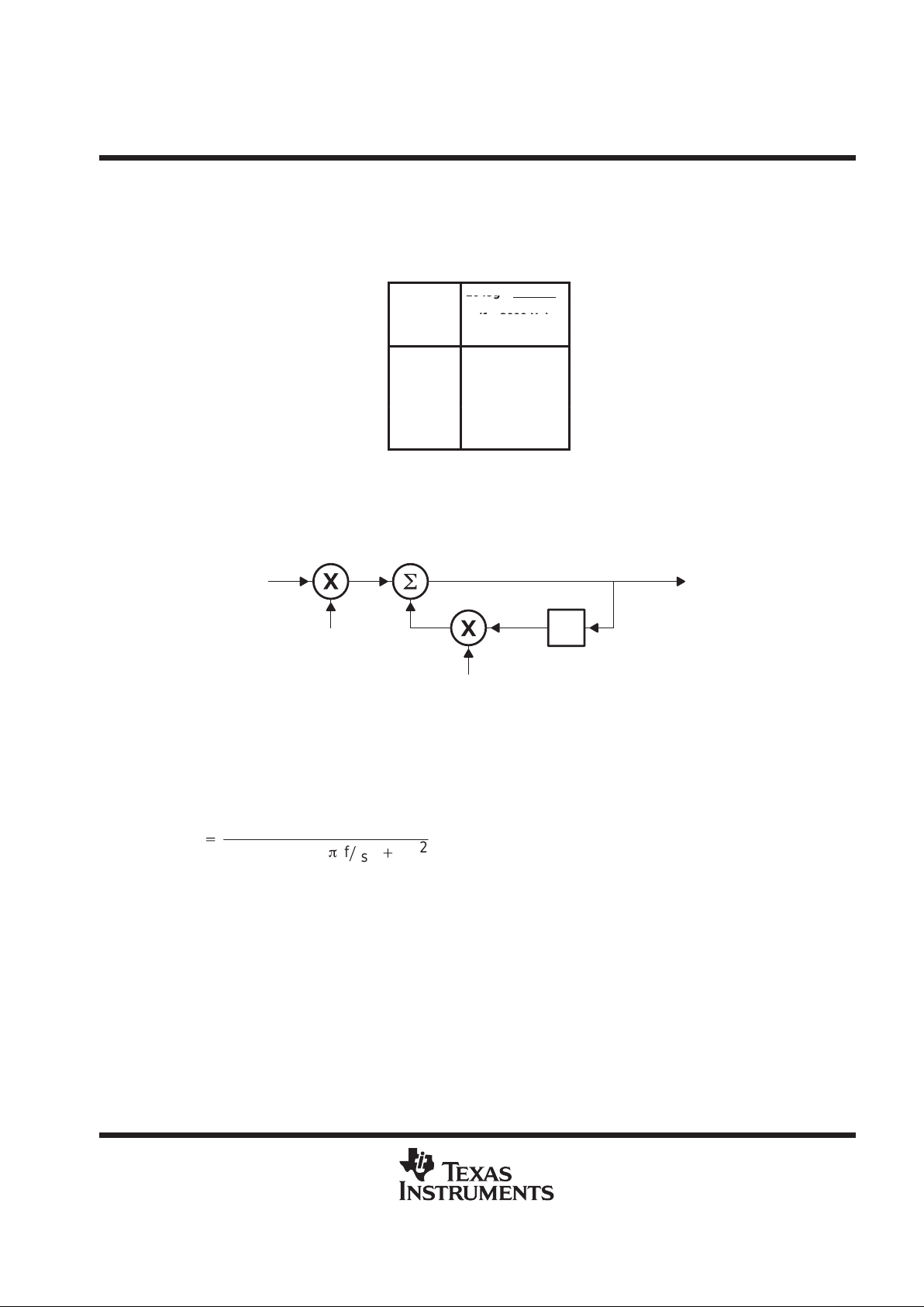
sin π f/f
s
π
f/f
s
TLC32044C, TLC32044E, TLC32044I, TLC32044M, TLC32045C, TLC32045I
VOICE-BAND ANALOG INTERFACE CIRCUITS
SLAS017F – MARCH 1988 – REVISED MA Y 1995
29
POST OFFICE BOX 655303 • DALLAS, TEXAS 75265
(sin x)/x roll-off for a zero-order hold function
The (sin x) /x roll-off for the AIC DAC zero-order hold function at a band-edge frequency of 3000 Hz for the
various sampling rates is shown in the table below.
Table 4. (sin x)/x Roll-Off
20 lo
g
20 log
f
s
(Hz)
(f = 3000 Hz)
(dB)
7200 –2.64
8000 –2.11
9600 –1.44
14400 –0.63
19200 –0.35
The actual AIC (sin x)/x roll-off will be slightly less than the above figures because the AIC has less than a 100%
duty cycle hold interval.
correction filter
T o compensate for the (sin x)/x roll-off of the AIC, a first-order correction filter (shown below) is recommended.
u(i +
1)
(1 – p1)P2
+
+
z – 1
y(i +
1)
p1
The difference equation for this correction filter is:
yi + 1 = p2(1 –p1) (u
i + 1
) + p1 yi
where the constant p1 determines the pole locations.
The resulting squared magnitude transfer function is:
p22(1–p1)
2
1 – 2p1 cos(2pfńfs))p1
2
|H(f)|2+
TLC32044C, TLC32044E, TLC32044I, TLC32044M, TLC32045C, TLC32045I
VOICE-BAND ANALOG INTERFACE CIRCUITS
SLAS017F – MARCH 1988 – REVISED MA Y 1995
30
POST OFFICE BOX 655303 • DALLAS, TEXAS 75265
correction results
Table 5 shows the optimum p values and the corresponding correction results for 8000-Hz and 9600-Hz
sampling rates.
T able 5. Optimum P Values
ERROR (dB)
fs = 8000 Hz
ERROR (dB)
fs = 9600 Hz
f (Hz)
s
p1 = –0.14813
p2 = 0.9888
s
p1 = –0.1307
p2 = 0.9951
300 –0.099 –0.043
600 –0.089 –0.043
900 –0.054 0
1200 –0.002 0
1500 0.041 0
1800 0.079 0.043
2100 0.100 0.043
2400 0.091 0.043
2700 –0.043 0
3000 –0.102 –0.043
TMS(SMJ)320 software requirements
The digital correction filter equation can be written in state variable form as follows:
Y = k1 × Y + k2 × U
where
k1 = p1
k2 = (1 – p1) × p2
Y = filter state
U = next I/O sample
The coefficients k1 and k2 must be represented as 16-bit integers. The SACH instruction (with the proper shift)
yields the correct result. With the assumption that the TMS(SMJ)320 processor page pointer and memory
configuration are properly initialized, the equation can be executed in seven instructions or seven cycles with
the following program:
ZAC
LT K2
MPY U
L TA K1
MPY Y
APAC
SACH (dma), (shift)
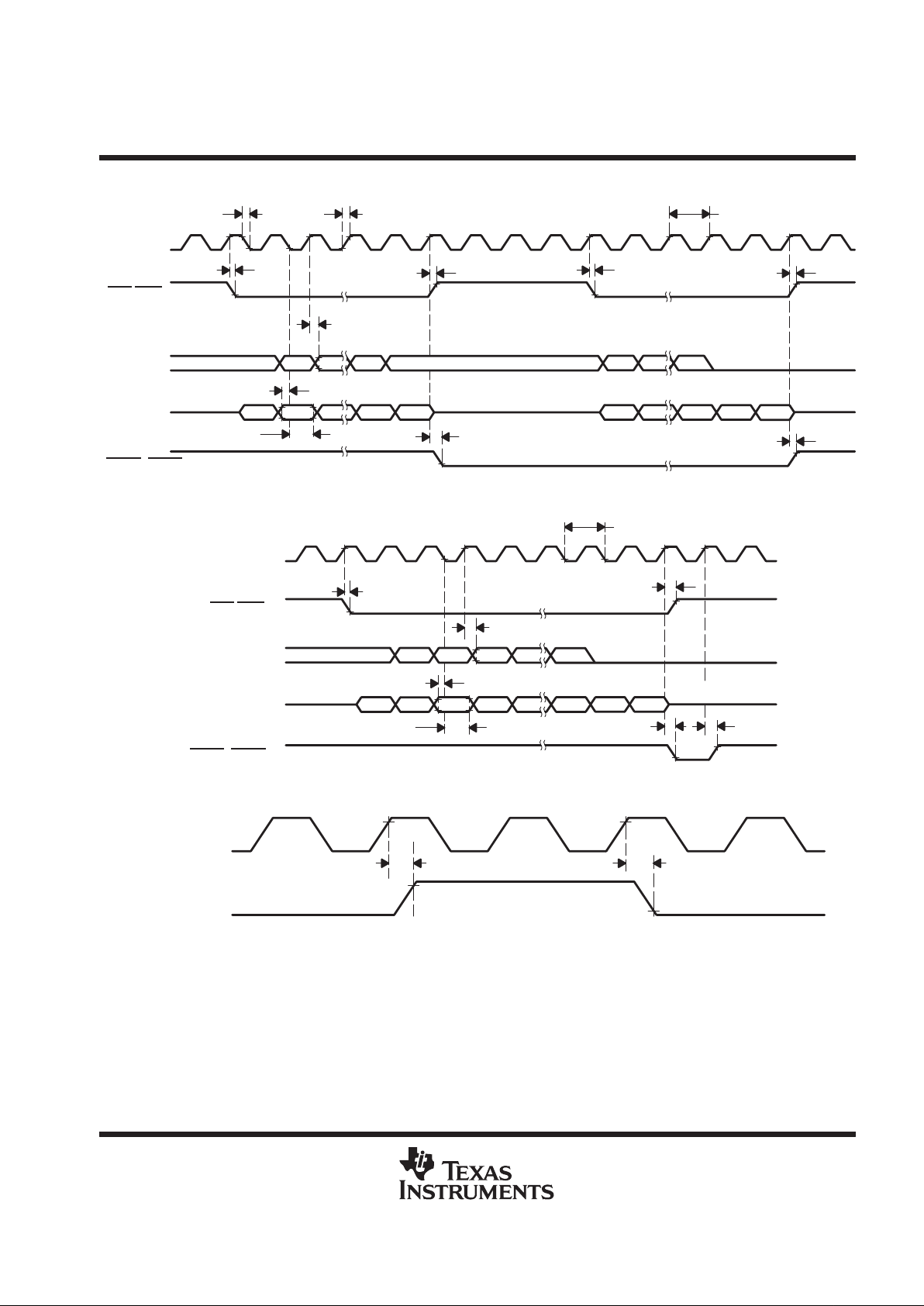
TLC32044C, TLC32044E, TLC32044I, TLC32044M, TLC32045C, TLC32045I
VOICE-BAND ANALOG INTERFACE CIRCUITS
SLAS017F – MARCH 1988 – REVISED MA Y 1995
31
POST OFFICE BOX 655303 • DALLAS, TEXAS 75265
PARAMETER MEASUREMENT INFORMATION
t
f(SCLK)
t
r(SCLK)
t
c(SCLK)
2 V 2 V 2 V 2 V 2 V 2 V 2 V
0.8 V 0.8 V
t
d(CH-FL)
t
d(CH-FH)
0.8 V
t
d(CH-FL)
t
d(CH-FH)
2 V
0.8 V
2 V
2 V
t
d(CH-DR)
t
su(DX)
t
h(DX)
t
d(CH-EL) t
d(CH-EH)
Don’t Care
SHIFT CLK
FSR, FSX
DR
DX
EODR
, EODX
0.8 V
2 V
D8D9D13D14D15
D9D13D14D15 D8 D7 D6 D2 D1 D0
D7 D6 D2 D1 D0
(a) BYTE-MODE TIMING
SHIFT CLK
FSR, FSX
DR
DX
EODX
, EODR
2 V 2 V
0.8 V
t
d(CH-FL)
t
d(CH-FH)
0.8 V
2 V
t
c(SCLK)
2 V 2 V
0.8 V 0.8 V
D12D13D14
D1 D0
D11
D2
D12D13D14D15 D11
D1
D0
D2
t
h(DX)
t
d(CH-EL)
t
d(CH-EH)
2 V
0.8 V
D15
t
su(DX)
Don’t Care
t
d(CH-DR)
(b) WORD-MODE TIMING
MSTR CLK
SHIFT CLK
t
d(MH-SH)
t
d(MH-SL)
(c) SHIFT-CLOCK TIMING
Figure 9. Serial-Port Timing

TLC32044C, TLC32044E, TLC32044I, TLC32044M, TLC32045C, TLC32045I
VOICE-BAND ANALOG INTERFACE CIRCUITS
SLAS017F – MARCH 1988 – REVISED MA Y 1995
32
POST OFFICE BOX 655303 • DALLAS, TEXAS 75265
PARAMETER MEASUREMENT INFORMATION
TMS32010/
SMJ32010
DEN
A0/PA0
A1/PA1
A2/PA2
D0–D15
WE
CLKOUT
INT
A
B
C
G1
SN74(54)LS138
D0–D15
D0–D7
D8–D15
Y1
Y0
G2
S0
G1
S1
Q
H
SRA-H
CLK
G
2
S0
G
1
S1
Q
H
SR
A-H
CLK
SN74LS74
Q1DC1DR
SHIFT CLK
TLC32044/
TLC32045
DX
FSX
MSTR CLK
EODX
SN74(54)LS299
C2
Q2D
SN74(54)LS299
Figure 10. TMS(SMJ)32010/TMS(SMJ)320C15/(SMJ320E15)-TLC32044/45 Interface Circuit
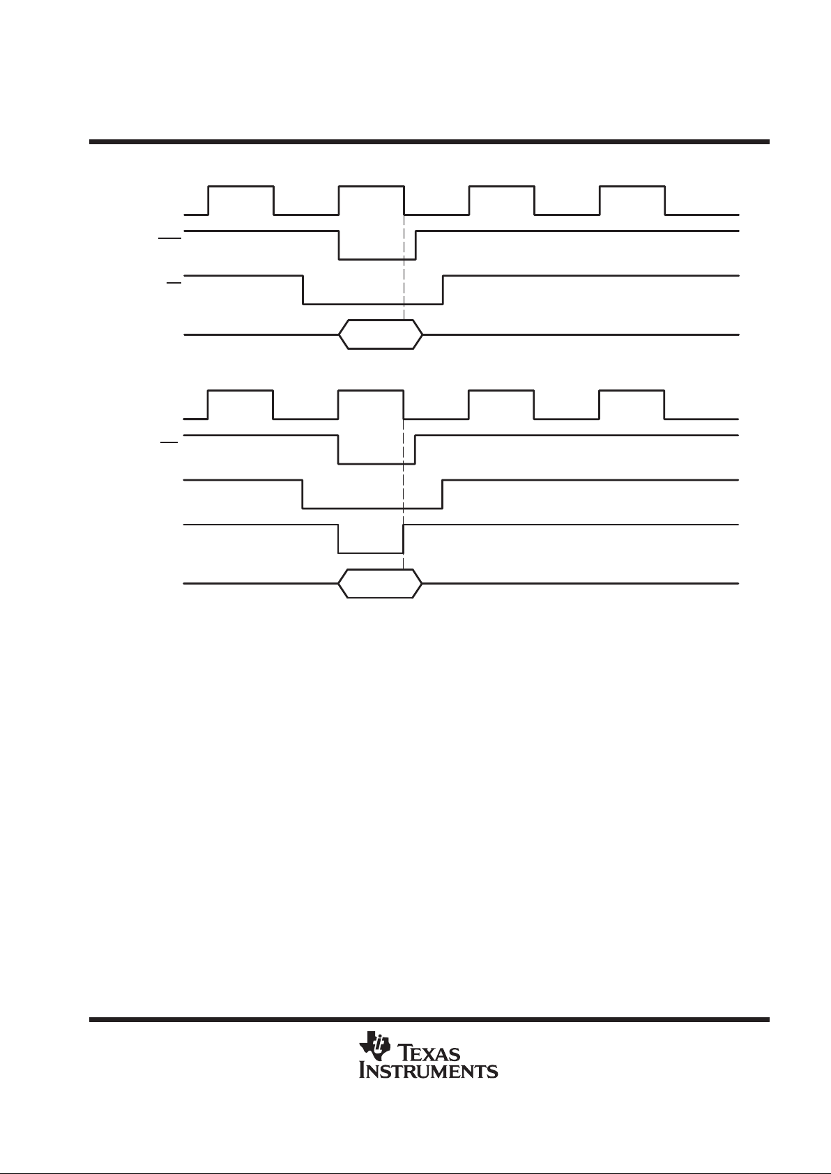
TLC32044C, TLC32044E, TLC32044I, TLC32044M, TLC32045C, TLC32045I
VOICE-BAND ANALOG INTERFACE CIRCUITS
SLAS017F – MARCH 1988 – REVISED MA Y 1995
33
POST OFFICE BOX 655303 • DALLAS, TEXAS 75265
PARAMETER MEASUREMENT INFORMATION
CLK OUT
DEN
S0, G1
D0–D15
Valid
(a) IN INSTRUCTION TIMING
CLK OUT
WE
SN74(54)LS299
CLK
D0–D15
Valid
SN74(54)LS138
Y1
(b) OUT INSTRUCTION TIMING
Figure 11. TMS(SMJ)32010/TMS(SMJ)320C15-TLC32044/TLC32045 Interface Timing
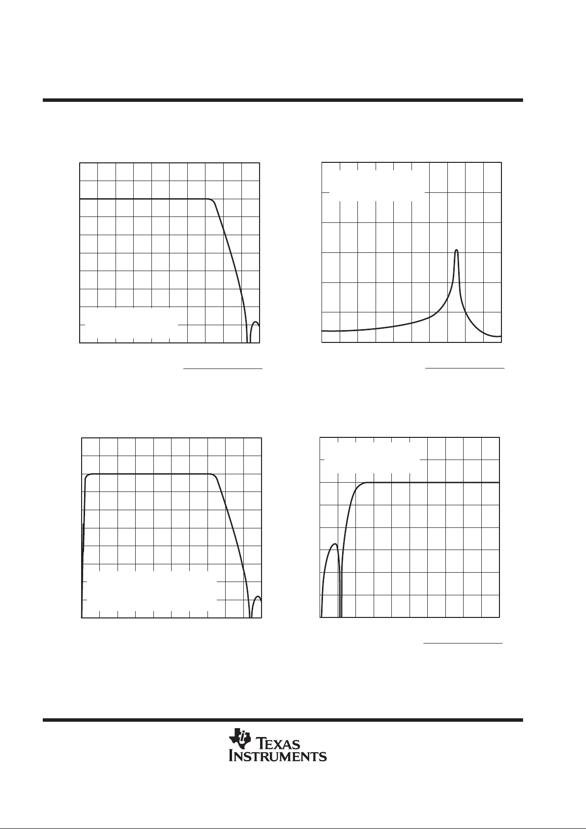
TLC32044C, TLC32044E, TLC32044I, TLC32044M, TLC32045C, TLC32045I
VOICE-BAND ANALOG INTERFACE CIRCUITS
SLAS017F – MARCH 1988 – REVISED MA Y 1995
34
POST OFFICE BOX 655303 • DALLAS, TEXAS 75265
TYPICAL CHARACTERISTICS
Figure 12
–60
–30
10
0 0.5 1 1.5 2 2.5 3
Magnitude – dB
–10
–20
0
20
3.5 4 4.5 5
Normalized Frequency – kHz ×
SCF Clock Frequency
288 kHz
AIC TRANSMIT AND RECEIVE
LOW-PASS FILTER
SCF Clock f = 288 kHz
TA = 25°C
Input = ±3-V Sine wave
–50
–40
–80
–70
Figure 13
AIC TRANSMIT AND RECEIVE
LOW-PASS FILTER
2.5
2
1
0.5
1.5
0 0.5 1 1.5 2 2.5 3
Group Delay – ms
3
3.5 4 4.5 5
Normalized Frequency – kHz ×
SCF Clock Frequency
288 kHz
SCF Clock f = 288 kHz
TA = 25°C
Input = ±3-V Sine wave
Figure 14
–50
–40
–60
–80
–30
10
0 0.5 1 1.5 2 2.5 3
Magnitude – dB
–10
–20
0
20
3.5 4 4.5 5
Frequency – kHz
AIC RECEIVE-CHANNEL
BANDPASS FILTER
Low-Pass SCF Clock f = 288 kHz
High-Pass SCF Clock f = 8 kHz
TA = 25°C
Input = ±3-V Sine wave
–70
Figure 15
–10
–20
–30
0 50 100 150 200 250 300
Magnitude – dB
0
AIC RECEIVE-CHANNEL
HIGH-PASS FILTER
350 400 450 500
Normalized Frequency – kHz ×
A/D Conversion Rate
8 k samples/s
10
20
SCF Clock f = 8 kHz
TA = 25°C
Input = ±3-V Sine wave
–50
–40
–60
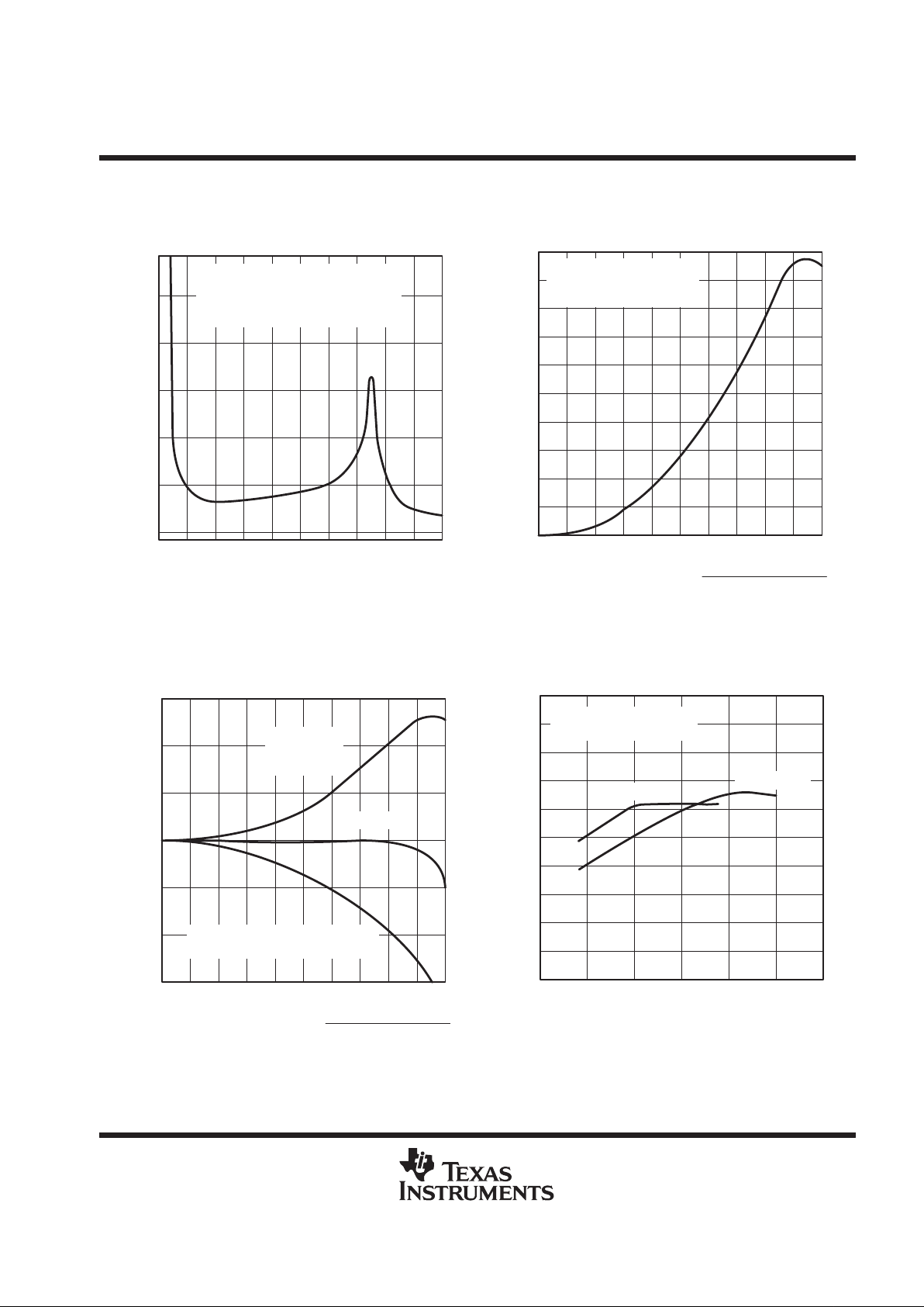
TLC32044C, TLC32044E, TLC32044I, TLC32044M, TLC32045C, TLC32045I
VOICE-BAND ANALOG INTERFACE CIRCUITS
SLAS017F – MARCH 1988 – REVISED MA Y 1995
35
POST OFFICE BOX 655303 • DALLAS, TEXAS 75265
TYPICAL CHARACTERISTICS
Figure 16
0.5 1 1.5 2 2.5 3 3.5 4 4.5 5
2.5
2.0
1.0
0.5
0.0
1.5
Group Delay – ms
AIC RECEIVE CHANNEL
BANDPASS FILTER
Frequency – kHz
Low-Pass SCF Clock f = 288 kHz
High-Pass SCF Clock f = 8 kHz
TA = 25°C
Input = ±3-V Sine wave
Figure 17
2.5
2
1
0.5
0
4.5
1.5
0.5 1 1.5 2 2.5 3
Magnitude – dB
3.5
3
4
5
3.5 4 4.5 5
Normalized Frequency – kHz ×
SCF Clock Frequency
288 kHz
AIC (sin x)/x CORRECTION FILTER
SCF Clock f = 288 kHz
TA = 25°C
Input = ±3-V Sine wave
Figure 18
4
2
–2
0
0 0.5 1 1.5 2 2.5 3
6
AIC (sin x)/x CORRECTION FILTER
3.5 4 4.5 5
Normalized Frequency – kHz ×
SCF Clock Frequency
288 kHz
Magnitude – dB
(sin x)/x
Correction
Filter
Error
D/A Converter (sin x)/x
Distortion for TB Register = 36
–4
–6
Figure 19
50
40
20
10
0
90
30
–10 0 10
Signal-to-Distortion Ratio – dB
70
60
80
100
A/D SIGNAL-TO-DISTORTION RATIO
vs
INPUT-SIGNAL LEVEL
Input Signal Relative to V
ref
– dB
1-kHz Input Signal
8-kHz Conversion Rate
Gain = 4x
Gain = 1x
–50 –40 –30 –20

TLC32044C, TLC32044E, TLC32044I, TLC32044M, TLC32045C, TLC32045I
VOICE-BAND ANALOG INTERFACE CIRCUITS
SLAS017F – MARCH 1988 – REVISED MA Y 1995
36
POST OFFICE BOX 655303 • DALLAS, TEXAS 75265
TYPICAL CHARACTERISTICS
Figure 20
–10 0 10
–50 –40 –30 –20
0
0.4
Gain Tracking – dB
0.2
0.1
0.3
0.5
Input Signal Relative to V
ref
– dB
A/D GAIN TRACKING
(GAIN RELATIVE TO GAIN
AT 0-dB INPUT-SIGNAL LEVEL)
1-kHz Input Signal
8-kHz Conversion Rate
–0.1
–0.2
–0.3
–0.4
–0.5
Figure 21
–10 0 10
–50 –40 –30 –20
50
40
20
10
0
90
30
Signal-to-Distortion Ratio – dB
70
60
80
100
D/A CONVERTER SIGNAL-TO-DISTORTION RATIO
vs
INPUT-SIGNAL LEVEL
Input Signal Relative to V
ref
– dB
1-kHz Input Signal into 600 Ω
8-kHz Conversion Rate
Figure 22
–10 0 10–50 –40 –30 –20
0
0.4
0.2
0.1
0.3
0.5
–0.1
–0.2
–0.3
–0.4
–0.5
Gain Tracking – dB
Input Signal Relative to V
ref
– dB
D/A GAIN TRACKING
(GAIN RELATIVE TO GAIN
AT 0-dB INPUT-SIGNAL LEVEL)
1-kHz Input Signal into 600 Ω
8-kHz Conversion Rate
Figure 23
Second Harmonic Distortion – dB
Input Signal Relative to V
ref
– dB
A/D SECOND HARMONIC DISTORTION
vs
INPUT-SIGNAL LEVEL
1-kHz Input Signal
8-kHz Conversion Rate
–10 0 10–50 –40 –30 –20
–100
–90
–80
–70
–60
–50
–40
–30
–20
–10
0

TLC32044C, TLC32044E, TLC32044I, TLC32044M, TLC32045C, TLC32045I
VOICE-BAND ANALOG INTERFACE CIRCUITS
SLAS017F – MARCH 1988 – REVISED MA Y 1995
37
POST OFFICE BOX 655303 • DALLAS, TEXAS 75265
TYPICAL CHARACTERISTICS
Figure 24
–10 0 10
–50 –40 –30 –20
–100
–90
–80
–70
–60
–50
–40
–30
–20
–10
0
Second Harmonic Distortion – dB
Input Signal Relative to V
ref
– dB
D/A SECOND HARMONIC DISTORTION
vs
INPUT-SIGNAL LEVEL
1-kHz Input Signal Into 600 Ω
8-kHz Conversion Rate
Figure 25
–10 0 10–50 –40 –30 –20
–100
–90
–80
–70
–60
–50
–40
–30
–20
–10
0
Third Harmonic Distortion – dB
Input Signal Relative to V
ref
– dB
A/D THIRD HARMONIC DISTORTION
vs
INPUT-SIGNAL LEVEL
1-kHz Input Signal
8-kHz Conversion Rate
–10 0 10–50 –40 –30 –20
–100
–90
–80
–70
–60
–50
–40
–30
–20
–10
0
Third Harmonic Distortion – dB
Input Signal Relative to V
ref
– dB
D/A THIRD HARMONIC DISTORTION
vs
INPUT-SIGNAL LEVEL
1-kHz Input Signal into 600 Ω
8-kHz Conversion Rate
Figure 26
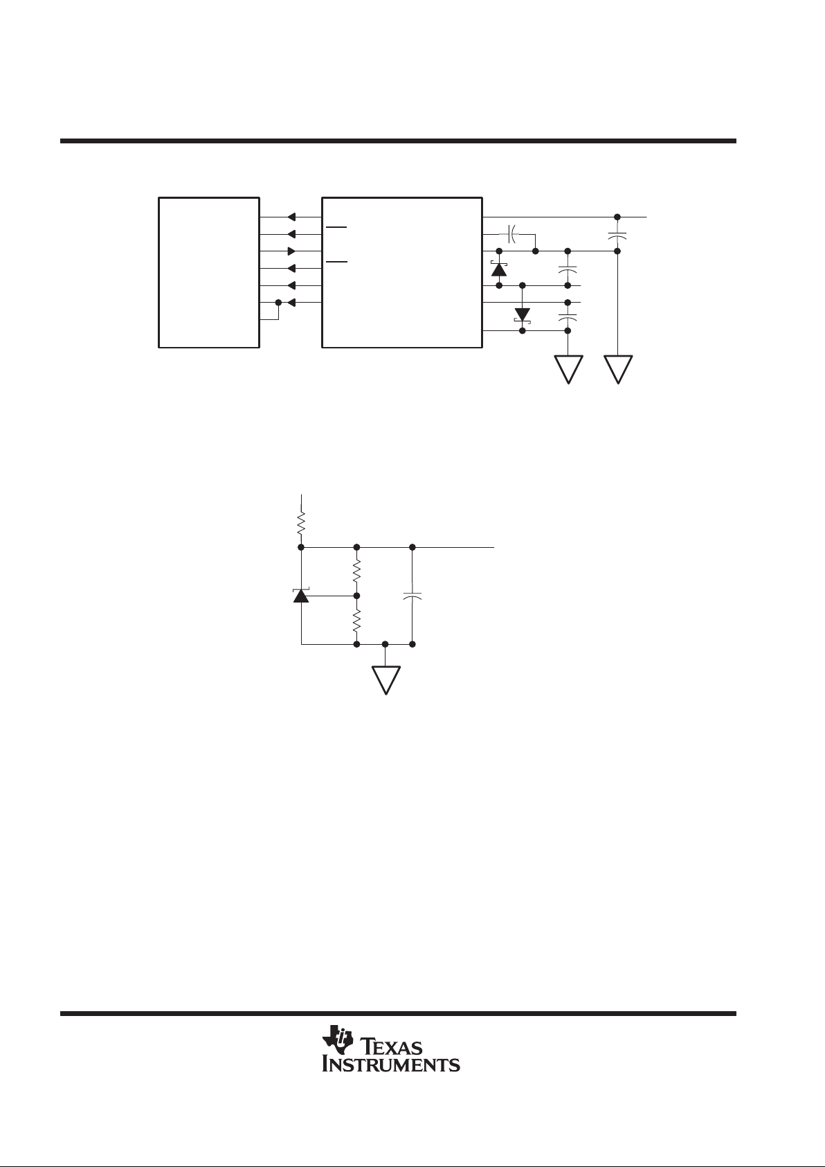
TLC32044C, TLC32044E, TLC32044I, TLC32044M, TLC32045C, TLC32045I
VOICE-BAND ANALOG INTERFACE CIRCUITS
SLAS017F – MARCH 1988 – REVISED MA Y 1995
38
POST OFFICE BOX 655303 • DALLAS, TEXAS 75265
APPLICATION INFORMATION
CLKOUT
FSX
DX
FSR
DR
CLKR
CLKX
MSTR CLK
FSX
DX
FSR
DR
SHIFT CLK
TMS(SMJ)32020/C25 TLC32044/TLC32045
V
CC+
REF
ANLG GND
V
CC–
V
DD
DGTL GND
BAT 42
†
C
C
C
–5 V
5 V
0.1 µF
D A
C = 0.2 µF, Ceramic
5 V
Figure 27. AIC Interface to the TMS(SMJ)32020/C25 Showing Decoupling Capacitors and Schottky Diode
†
†
Thomson Semiconductors
D
V
CC
R
TL431
500 Ω
2500 Ω
0.01 µF
3-V Output
For:
VCC = 12 V, R = 7200 Ω
VCC = 10 V, R = 5600 Ω
VCC = 5 V, R = 1600 Ω
Figure 28. External Reference Circuit For TLC32044/TLC32045

IMPORTANT NOTICE
T exas Instruments and its subsidiaries (TI) reserve the right to make changes to their products or to discontinue
any product or service without notice, and advise customers to obtain the latest version of relevant information
to verify, before placing orders, that information being relied on is current and complete. All products are sold
subject to the terms and conditions of sale supplied at the time of order acknowledgement, including those
pertaining to warranty, patent infringement, and limitation of liability.
TI warrants performance of its semiconductor products to the specifications applicable at the time of sale in
accordance with TI’s standard warranty. Testing and other quality control techniques are utilized to the extent
TI deems necessary to support this warranty. Specific testing of all parameters of each device is not necessarily
performed, except those mandated by government requirements.
CERT AIN APPLICATIONS USING SEMICONDUCTOR PRODUCTS MAY INVOLVE POTENTIAL RISKS OF
DEATH, PERSONAL INJURY, OR SEVERE PROPERTY OR ENVIRONMENTAL DAMAGE (“CRITICAL
APPLICATIONS”). TI SEMICONDUCTOR PRODUCTS ARE NOT DESIGNED, AUTHORIZED, OR
WARRANTED TO BE SUITABLE FOR USE IN LIFE-SUPPORT DEVICES OR SYSTEMS OR OTHER
CRITICAL APPLICATIONS. INCLUSION OF TI PRODUCTS IN SUCH APPLICA TIONS IS UNDERST OOD TO
BE FULLY AT THE CUSTOMER’S RISK.
In order to minimize risks associated with the customer’s applications, adequate design and operating
safeguards must be provided by the customer to minimize inherent or procedural hazards.
TI assumes no liability for applications assistance or customer product design. TI does not warrant or represent
that any license, either express or implied, is granted under any patent right, copyright, mask work right, or other
intellectual property right of TI covering or relating to any combination, machine, or process in which such
semiconductor products or services might be or are used. TI’s publication of information regarding any third
party’s products or services does not constitute TI’s approval, warranty or endorsement thereof.
Copyright 1998, Texas Instruments Incorporated
 Loading...