TLC32040M
ANALOG INTERFACE CIRCUIT
SGLS031 – MAY 1990
• Advanced LinCMOS Silicon-Gate Process
Technology
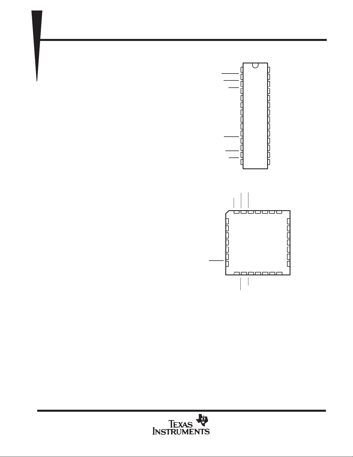
J PACKAGE
(TOP VIEW)
• 14-Bit Dynamic Range ADC and DAC
NU
FSR
DR
V
DD
REF
DX
FSX
1
2
3
4
5
6
7
8
9
10
11
12
13
14
• Variable ADC and DAC Sampling Rate up to
19200 Samples Per Second
• Switched-Capacitor Antialiasing Input Filter
and Output-Reconstruction Filter
• Serial Port for Direct Interface to
SMJ320E14, SMJ32020, SMJ320C25, and
SMJ320C30 Digital Processors
• Synchronous or Asynchronous ADC and
DAC Conversion Rates With Programmable
Incremental ADC and DAC Conversion
Timing Adjustments
• Serial Port Interface to SN54299
Serial-to-Parallel Shift Register for Parallel
RESET
EODR
MSTR CLK
DGTL GND
SHIFT CLK
EODX
WORD/BYTE
Interface to SMJ320C10, SMJ320C15,
SMJ320E15, or Other Digital Processors
description
FK PACKAGE
(TOP VIEW)
The TLC32040M interface circuit is a complete
EODR
FSR
analog-to-digital and digital-to-analog input/
output system on a single monolithic CMOS
chip. This device integrates a band-pass
switched-capacitor antialiasing input filter, a
14-bit-resolution A/D converter, four
microprocessor-compatible serial port modes, a
14-bit-resolution D/A converter, and a low-pass
switched-capacitor output reconstruction filter.
The device offers numerous combinations of
master clock input frequencies and conversion/
DR
MSTR CLK
V
DD
REF
DGTL GND
SHIFT CLK
EODX
5
6
7
8
9
10
11
12 13
RESETNUNUNUIN+
3212827
426
14 15 16 1718
sampling rates, which can be changed via digital
processor control.
DX
FSX
Typical applications for this integrated circuit
include modems (7.2-, 8-, 9.6-, 14.4-, and
19.2-kHz sampling rate), analog interface for
digital signal processors (DSPs), speech recognition/storage systems, industrial process control, biomedical
instrumentation, acoustical signal processing, spectral analysis, data acquisition, and instrumentation
NU–Nonusable; no external connection should be made to
these pins.
WORD/BYTE
recorders. Four serial modes, which allow direct interface to the SMJ320E14, SMJ32020, SMJ320C25, and
SMJ320C30 digital signal processors, are provided. Also, when the transmit and receive sections of the analog
interface circuit (AIC) are operating synchronously, it will interface to two SN54299 serial-to-parallel shift
registers.These serial-to-parallel shift registers can then interface in parallel to the SMJ320C10, SMJ320C15,
SMJ320E15, other digital signal processors, or external FIFO circuitry . Output data pulses are emitted to inform
the processor that data transmission is complete or to allow the DSP to differentiate between two transmitted
bytes. A flexible control scheme is provided so that the functions of the integrated circuit can be selected and
adjusted coincidentally with signal processing via software control.
28
27
26
25
24
23
22
21
20
19
18
17
16
15
NU
NU
NU
NU
IN+
IN–
AUX IN+
AUX IN–
OUT+
OUT–
V
CC+
V
CC–
ANLG GND
ANLG GND
NU
NU
IN–
25
AUX IN+
24
AUX IN–
23
OUT+
22
OUT–
21
V
20
V
19
ANLG GND
ANLG GND
CC+
CC–
Advanced LinCMOS is a trademark of Texas Instruments Incorporated.
PRODUCTION DATA information is current as of publication date.
Products conform to specifications per the terms of Texas Instruments
standard warranty. Production processing does not necessarily include
testing of all parameters.
POST OFFICE BOX 655303 • DALLAS, TEXAS 75265
Copyright 1990, Texas Instruments Incorporated
4–1
TLC32040M
ANALOG INTERFACE CIRCUIT
description (continued)
The antialiasing input filter comprises seventh-order and fourth-order CC-type (Chebyshev/elliptic transitional)
low-pass and high-pass filters, respectively, and a fourth-order equalizer. The input filter is implemented in
switched-capacitor technology and is preceded by a continuous time filter to eliminate any possibility of aliasing
caused by sampled data filtering. When no filtering is desired, the entire composite filter can be switched out
of the signal path. A selectable, auxiliary , differential analog input is provided for applications where more than
one analog input is required.
The A/D and D/A converters each have 14 bits of resolution. The A/D and D/A architectures ensure no missing
codes and monotonic operation. An internal voltage reference is provided on the TLC32040M to ease the design
task and to provide complete control over the performance of the integrated circuit. The internal voltage
reference is brought out to a pin and is available to the designer. Separate analog and digital voltage supplies
and grounds are provided to minimize noise and ensure a wide dynamic range. Also, the analog circuit path
contains only differential circuitry to keep noise to an absolute minimum. The only exception is the DAC sample
and hold, which utilizes pseudo-differential circuitry.
The output-reconstruction filter is a seventh-order CC-type (Chebyshev/elliptic transitional low-pass filter with
a fourth-order equalizer) and is implemented in switched-capacitor technology. This filter is followed by a
continuous-time filter to eliminate images of the digitally encoded signal.
The TLC32040M is characterized for operation from –55°C to 125°C.
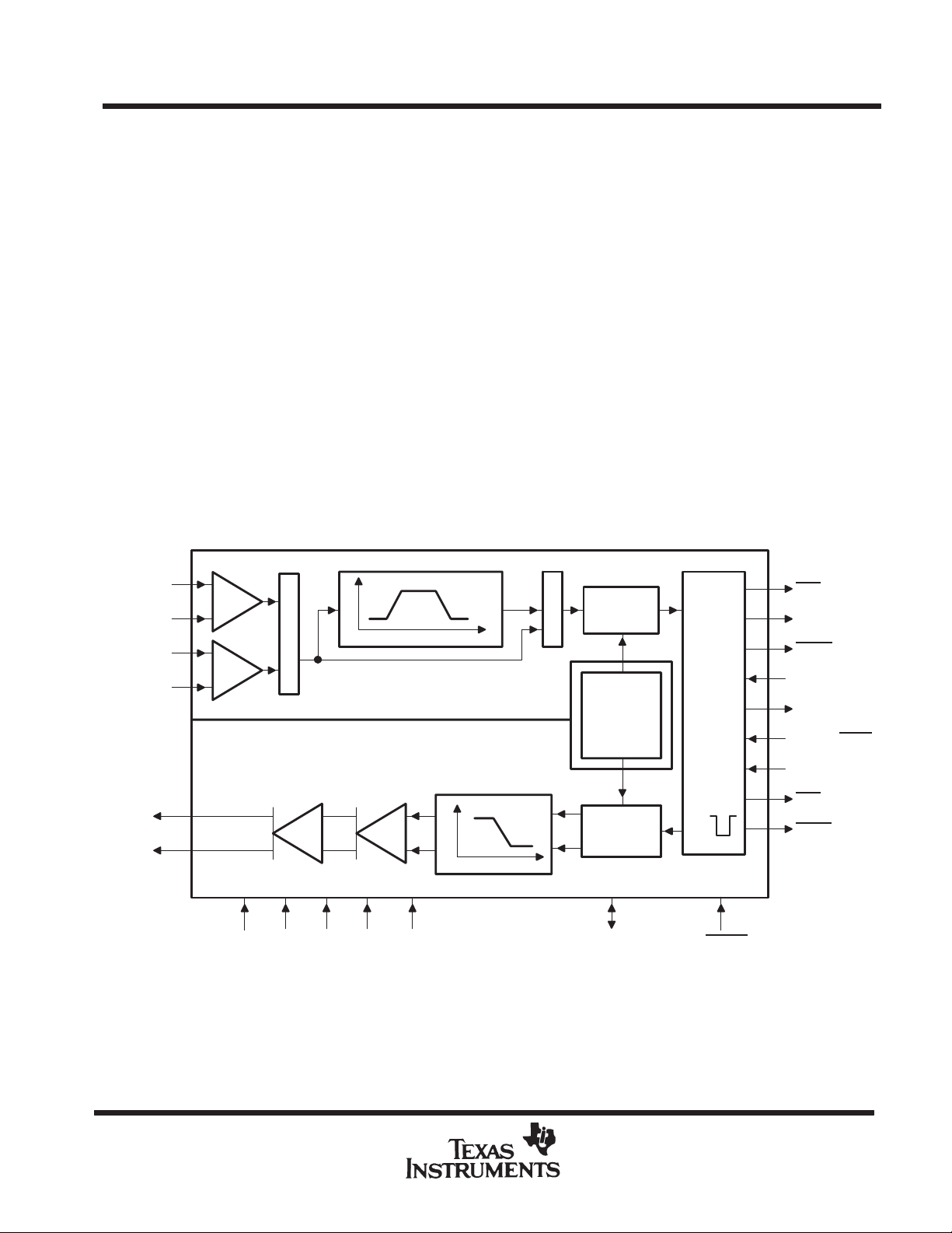
functional block diagram
26
IN+
OUT+
OUT–
IN–
AUX
IN+
AUX
IN–
25
24
23
22
21
20
V
M
U
X
19
CC+VCC–
+
–
18
ANLG
GND
Band-Pass Filter
Receive Section
+
–
Transmit Section
9
DTGL
GND
7
V
DD
(DIG)
Low-Pass Filter
M
U
X
Serial
A/D
Internal
Voltage
Reference
D/A
8
REF RESET
Port
2
4
FSR
5
DR
3
EODR
6
MSTR CLK
10
SHIFT CLK
13
WORD/BYTE
12
DX
14
FSX
11
EODX
4–2
POST OFFICE BOX 655303 • DALLAS, TEXAS 75265
Terminal Functions
TLC32040M
ANALOG INTERFACE CIRCUIT
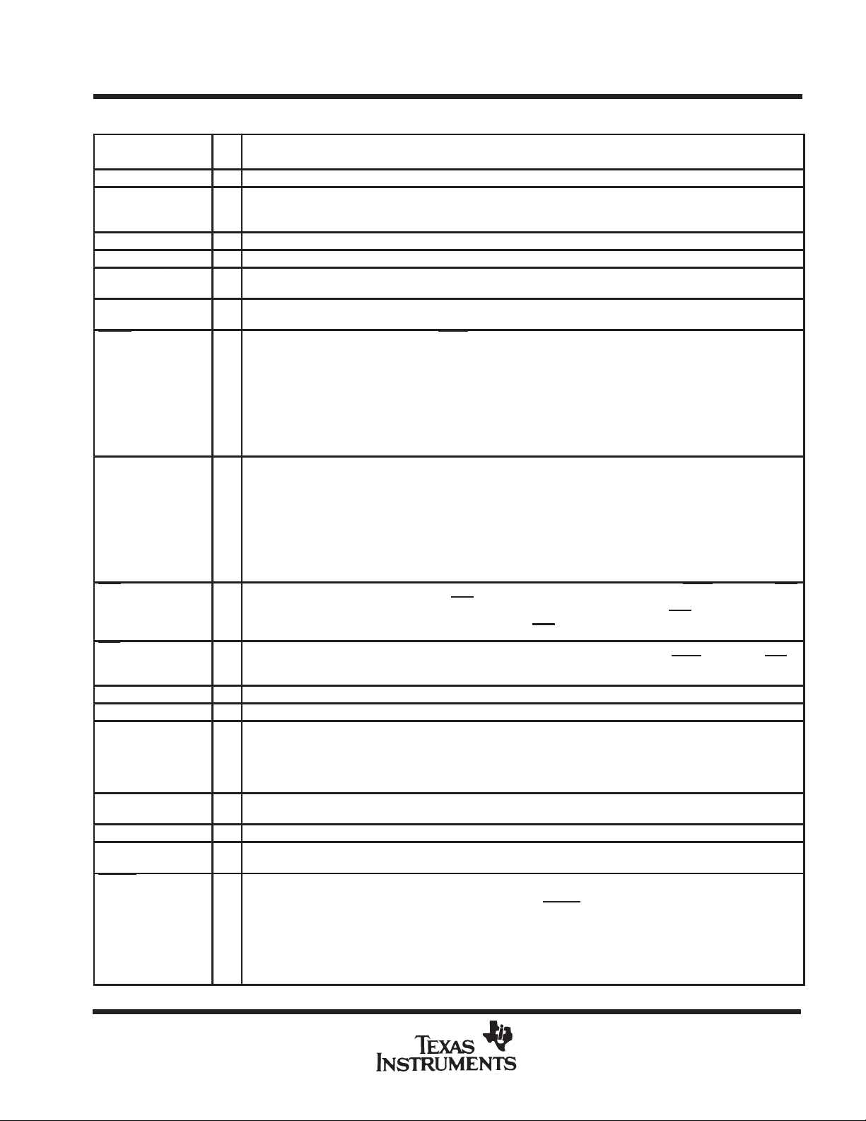
PIN
NAME NO.
ANLG GND 17, 18 Analog ground return for all internal analog circuits. Not internally connected to DGTL GND.
AUX IN+ 24 I Noninverting auxiliary analog input stage. This input can be switched into the band-pass filter and A/D converter
AUX IN– 23 I Inverting auxiliary analog input (see the above AUX IN+ pin description).
DGTL GND 9 Digital ground for all internal logic circuits. Not internally connected to ANLG GND.
DR 5 O This pin is used to transmit the ADC output bits from the AIC to the TMS320 serial port. This transmission of bits
DX 12 I This pin is used to receive the DAC input bits and timing and control information from the TMS320. This serial
EODR 3 O End of data receive.(See the WORD/BYTE pin description and the Serial Port TIming dIagram.) During the
EODX 11 O End of data transmit. See WORD/BYTE description and Serial Port Timing diagram. During the word-mode timing,
FSR 4 O Frame sync receive. In the serial transmission modes, which are described in the WORD/BYTE description, FSR
FSX 14 O Frame sync transmit. When this terminal goes low, the SMJ320 serial port will begin transmitting bits to the AIC
IN+ 26 I Noninverting input to analog input amplifier stage
IN– 25 I Inverting input to analog input amplifier stage
MSTR CLK 6 I The master clock signal is used to derive all the key logic signals of the AIC, such as the shift clock, the
OUT+ 22 O Noninverting output of analog output power amplifier. Can drive transformer hybrids or high-impedance loads
OUT– 21 O Inverting output of analog output power amplifier. Functionally identical with and complementary to OUT+.
REF 8 I/O The internal voltage reference is brought out on this terminal. Also an external voltage reference can be applied
RESET 2 I A reset function is provided to initialize the TA, TA’, TB, RA, RA’, RB, and control registers. This reset function
I/O
path via software control. If the appropriate bit in the control register is a 1, the auxiliary inputs will replace the IN+
and IN– inputs. If the bit is a 0, the IN+ and IN– inputs will be used (see the AIC DX data word format section).
from the AIC to the TMS320 serial port is synchronized with the SHIFT CLK signal.
transmission from the TMS320 serial port to the AIC is synchronized with the SHIFT CLK signal.
word-mode timing, this signal is a low-going pulse that occurs immediately after the 16 bits of A/D information have
been transmitted from the AIC to the TMS320 serial port. This signal can be used to interrupt a microprocessor
upon completion of serial communications. Also, this signal can be used to strobe and enable external
serial-to-parallel shift registers, latches, or external FIFO RAM, and to facilitate parallel data bus communications
between the AIC and the serial-to-parallel shift registers. During the byte-mode timing, this signal goes low after
the first byte has been transmitted from the AIC to the TMS320 serial port and is kept low until the second byte
has been transmitted. The TMS3201 1 or TMS320C17 can use this low-going signal to dif ferentiate between the
two bytes as to which is first and which is second.
this signal is a low-going pulse that occurs immediately after the 16 bits of D/A converter and control or register
information have been transmitted from the SMJ320 serial port to the AIC. This signal can be used to interrupt a
microprocessor upon the completion of serial communications. Also, this signal can be used to strobe and enable
external serial-to-parallel shift registers, latches, or an external FIFO RAM, and to facilitate parallel data-bus
communications between the AIC and the serial-to-parallel shift registers. During the byte-mode timing, this signal
goes low after the first byte has been transmitted from the SMJ320 serial port to the AIC and is kept low until the
second byte has been transmitted. The DSP can use this low-going signal to differentiate between the two bytes
as to which is first and which is second.
is held low during bit transmission. When FSR goes low, the SMJ320 serial port will begin receiving bits from the
AIC via the DR pin of the AIC. The most significant DR bit will be present on DR before FSR
Port Timing and Internal Timing Configuration diagrams.) FSR
via DX of the AIC. In all serial transmission modes, which are described in the WORD/BYTE
held low during bit transmission (see the Serial Port Timing and Internal Timing Configuration diagrams).
switched-capacitor filter clocks, and the A/D and D/A timing signals. The Internal Timing Configuration diagram
shows how these key signals are derived. The frequencies of these key signals are synchronous submultiples of
the master clock frequency to eliminate unwanted aliasing when the sampled analog signals are transferred
between the switched-capacitor filters and the A/D and D/A converters (see the Internal Timing Configuration).
directly in either a differential or a single-ended configuration.
to this terminal.
initiates serial communications between the AIC and DSP. The reset function will initialize all AIC registers
including the control register. After a negative-going pulse on RESET
an 8-kHz data conversion rate for a 5.184-MHz master clock input signal. The conversion rate adjust registers,
TA’ and RA’, will be reset to 1. The control register bits will be reset as follows (see AIC DX data word format
section).
d7 = 1, d6 = 1, d5 = 1, d4 = 0, d3 = 0, d2 = 1
This initialization allows normal serial-port communication to occur between the AIC and the DSP.
DESCRIPTION
goes low. (See Serial
does not occur after secondary communication.
description, FSX is
, the AIC registers will be initialized to provide
POST OFFICE BOX 655303 • DALLAS, TEXAS 75265
4–3
TLC32040M
ANALOG INTERFACE CIRCUIT
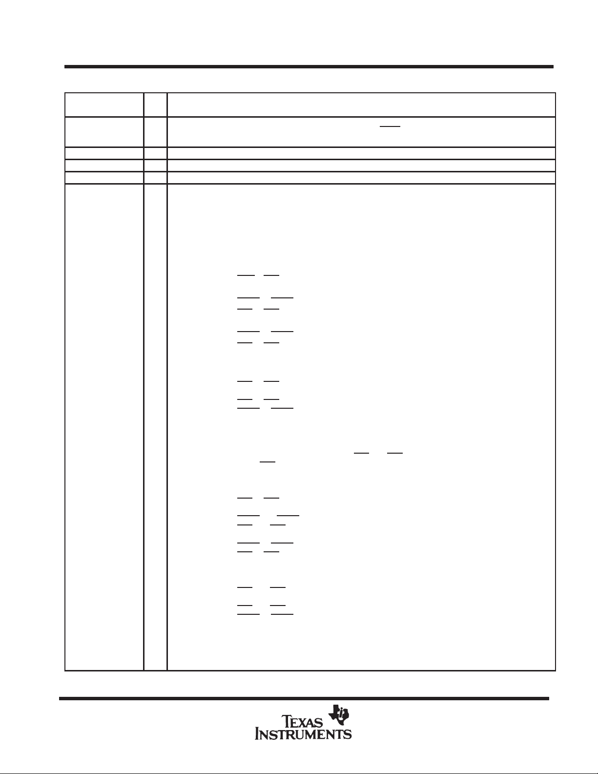
Terminal Functions (Continued)
PIN
NAME NO.
SHIFT CLK 10 O The shift clock signal is obtained by dividing the master clock signal frequency by four. This signal is used to clock
V
DD
V
CC+
V
CC–
WORD/BYTE 13 I
I/O
the serial data transfers of the AIC, described in the WORD/BYTE description (see the Serial Port Timing and
Internal Timing Configuration diagrams).
7 Digital supply voltage, 5 V ±5%
20 Positive analog supply voltage, 5 V ±5%
19 Negative analog supply voltage, –5 V ±5%
This terminal, in conjunction with a bit in the control register, is used to establish one of four serial modes. These
four modes are described below.
AIC transmit and receive sections are operated asynchronously.
The following description applies when the AIC is configured to have asynchronous transmit and receive sections.
If the appropriate data bit in the control register is a 0 (see the AIC DX data word format), the transmit and receive
sections will be asynchronous.
L Serial port directly interfaces with the serial port of the DSP and communicates in two 8-bit bytes.
The operation sequence is as follows (see Serial Port Timing diagrams)
1. FSX or FSR is brought low.
2. One 8-bit byte is transmitted or one 8-bit byte is received.
3. EODX or EODR is brought low.
4. FSX
5. One 8-bit byte is transmitted or one 8-bit byte is received.
6. EODX
7. FSX
H Serial port directly interfaces with the serial port of the SMJ32020, SMJ320C25, or SMJ320C30 and
communicates in one 16-bit word. The operation sequence is as follows (see Serial Port Timing
diagrams):
1. FSX
2. One 16-bit word is transmitted or one 16-bit word is received.
3. FSX
4 EODX or EODR emits a low-going pulse.
AIC transmit and receive sections are operated synchronously.
If the appropriate data bit in the control register is a 1, the transmit and receive sections will be configured to be
synchronous. In this case, the band-pass switched-capacitor filter and the A/D conversion timing will be derived
from TX Counter A, TX Counter B, and TA, TA’, and TB registers, rather than the RX Counter A, RX Counter B,
and RA, RA’, and RB registers. In this case, the AIC FSX and FSR timing will be identical during primary data
communication; however , FSR will not be asserted during secondary data communication since there is no new
A/D conversion result. The synchronous operation sequences are as follows (see Serial Port Timing diagrams ).
L Serial port directly interfaces with the serial port of the DSP and communicates in two 8-bit bytes. The
operation sequence is as follows (see Serial Port Timing diagrams).
1. FSX or FSR are brought low.
2. One 8-bit byte is transmitted and one 8-bit byte is received.
3. EODX
4. FSX and FSR emit positive frame-sync pulse that are four shift-clock cycles wide.
5. One 8-bit byte is transmitted and one 8-bit byte is received.
6. EODX or EODR are brought high.
7. FSX or FSR are brought high.
H Serial port directly interfaces with the serial port of the SMJ32020, SMJ320C25, or SMJ320C30 and
communicates in one 16-bit word. The operation sequence is as follows (see Serial Port Timing
diagrams):
1. FSX
2. One 16-bit word is transmitted and one 16-bit word is received.
3. FSX and FSR are brought high.
4. EODX or EODR emit low-going pulses.
Since the transmit and receive sections of the AIC are now synchronous, the AIC serial port, with additional NOR
and AND gates, will interface to two SN54299 serial-to-parallel shift registers. Interfacing the AIC to the SN54299
shift register allows the AIC to interface to an external FIFO RAM and facilitates parallel data bus communications
between the AIC and the digital signal processor. The operation sequence is the same as the above sequence
(see Serial Port Timing diagrams).
or FSR emits a positive frame-sync pulse that is four shift-clock cycles wide.
or EODR is brought high.
or FSR is brought high.
or FSR is brought low.
or FSR is brought high.
and EODR are brought low.
and FSR are brought low.
DESCRIPTION
.
4–4
POST OFFICE BOX 655303 • DALLAS, TEXAS 75265
ANALOG INTERFACE CIRCUIT
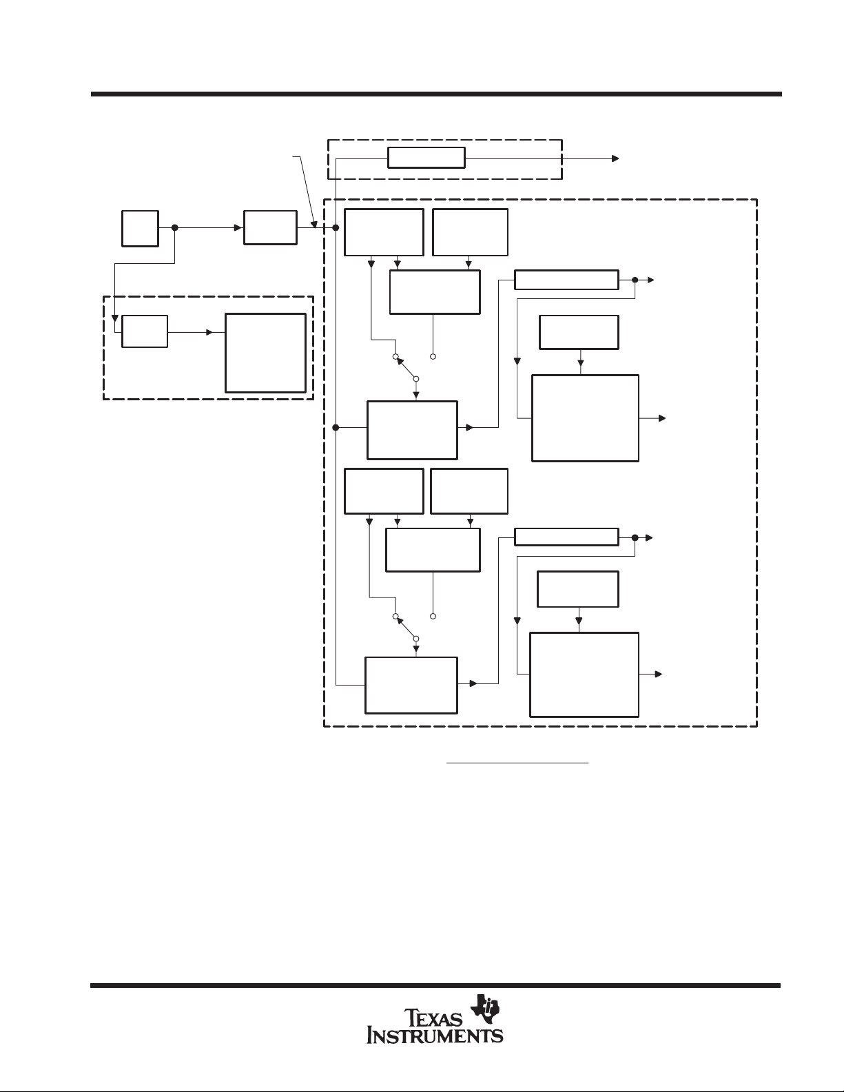
INTERNAL TIMING CONFIGURATION
TLC32040M
Master Clock
5.184 MHZ (1)
10.368 MHZ (2)
20.736 MHz (1)
41.472 MHz (2)
XTAL
Osc
Optional External Circuitry
for Full-Duplex Modems
153.6 kHz
Clock (1)
Divide
by 135
TMS320
DSP
Commercial
External
Front-End
Full-Duplex
Split-Band
Filters
TA Register
(5 Bits)
d0, d1 = 0,0
d0, d1 = 1, 1‡
TX Counter A
[TA = 9 (1)]
[TA = 18 (2)]
(6 Bits)
RA Register
(5 Bits)
Divide by 4
TA’ Register
Adder/
Subtractor
(6 Bits)
d0, d1 = 0,1
d0, d1 = 1,0‡
RA’ Register
Adder/
Subtractor
(6 Bits)
(6 Bits)
(2s Compl)
576-kHz
Pulses
(6 Bits)
(2s Compl)
Divide by 2
TB Register
(6 Bits)
TX Counter B
TB = 40, 7.2 kHz
TB = 36, 8.0 kHz
TB = 30, 9.6 kHz
TB = 20, 14.4 kHz
TB = 15, 19.2 kHz
Divide by 2
RB Register
(6 Bits)
Shift Clock
1.296 MHz (1)
2.592 MHz (2)
Low-Pass
Switched
Cap Filter
CLK = 288 kHz
Square Wave
D/A
Conversion
Frequency
Band-Pass
Switched
Cap Filter
CLK = 288 kHz
Square Wave
d0, d1 = 0,0
d0, d1 =
1,1‡
RX Counter A
[TA = 9 (1)]
[TA = 18 (2)]
(6 Bits)
SCF Clock Frequency =
†
Split-band filtering can alternatively be performed after the analog input function via software in the SMJ320.
‡
These control bits are described in the AIC DX data word format section.
d0, d1 = 0,1
d0, d1 = 1,0‡
576-kHz
Pulses
RX Counter B
RB = 40, 7.2 kHz
RB = 36, 8.0 kHz
RB = 30, 9.6 kHz
RB = 20, 14.4 kHz
RB = 15, 19.2 kHz
Master Clock Frequency
2 × Contents of Counter A
A/D
Conversion
Frequency
NOTE: Frequency 1, 20.736 MHz is used to show how 153.6 kHz (for a commercially available modem split-band filter clock), popular speech
and modem sampling signal frequencies, and an internal 288-kHz switched-capacitor filter clock can be derived synchronously and as
submultiples of the crystal oscillator frequency . Since these derived frequencies are synchronous submultiples of the crystal frequency,
aliasing does not occur as the sampled analog signal passes between the analog converter and switched-capacitor filter stages.
Frequency 2, 41.472 MHz is used to show that the AIC can work with high-frequency signals, which are used by high-speed digital signal
processors
.
POST OFFICE BOX 655303 • DALLAS, TEXAS 75265
4–5

TLC32040M
ANALOG INTERFACE CIRCUIT
explanation of internal timing configuration
All of the internal timing of the AIC is derived from the high-frequency clock signal that drives the master clock
input. The shift clock signal, which strobes the serial port data between the AIC and DSP, is derived by dividing
the master clock input signal frequency by four.
SCF Clock Frequency
Conversion Frequency
Shift Clock Frequency
TX Counter A and TX Counter B, which are driven by the master clock signal, determine the D/A conversion
timing. Similarly, RX Counter A and RX Counter B determine the A/D conversion timing. In order for the
switched-capacitor low-pass and band-pass filters to meet their transfer function specifications, the frequency
of the clock inputs of the switched-capacitor filters must be 288 kHz. If the frequencies of the clock inputs are
not 288 kHz , the filter transfer function frequencies are scaled by the ratios of the clock frequencies to 288 kHz.
Thus, to obtain the specified filter responses, the combination of master clock frequency and TX Counter A and
RX Counter A values must yield 288-kHz switched-capacitor clock signals. These 288-kHz clock signals can
then be divided by TX Counter B and RX Counter B to establish the D/A and A/D conversion timings.
TX Counter A and TX Counter B are reloaded every D/A conversion period, while RX Counter A and RX Counter
B are reloaded every A/D conversion period. TX Counter B and RX Counter B are loaded with the values in the
TB and RB Registers, respectively . V ia software control, TX Counter A can be loaded with either TA Register,
the T A Register less the T A ’ Register , or the T A Register plus the T A ’ Register . By selecting the T A Register less
the T A’ Register option, the upcoming conversion timing will occur earlier by an amount of time that equals TA’
times the signal period of the master clock. By selecting the TA Register plus the TA’ Register option, the
upcoming conversion timing will occur later by an amount of time that equals T A’ times the signal period of the
master clock. Thus the D/A conversion timing can be advanced or retarded. An identical ability to alter the A/D
conversion timing is provided. In this case, however, the RX Counter A can be programmed via software control
with the RA Register, the RA Register less the RA’ Register, or the RA Register plus the RA’ Register.
Master Clock Frequency
+
2 Contents of Counter A
SCF Clock Frequency
+
Contents of Counter B
Master Clock Frequency
+
4
The ability to advance or retard conversion timing is particularly useful for modem applications. This feature
allows controlled changes in the A/D and D/A conversion timing. This feature can be used to enhance signal-tonoise performance, to perform frequency-tracking functions, and to generate nonstandard modem frequencies.
If the transmit and receive sections are configured to be synchronous (see the WORD/BYTE
Terminal Functions table), then both the low-pass and band-pass switched-capacitor filter clocks are derived
from TX Counter A. Also, both the D/A and A/D conversion timing are derived from TX Counter A and TX Counter
B. When the transmit and receive sections are configured to be synchronous, the RX Counter A, RX Counter
B, RA Register, RA’ Register, and RB Registers are not used.
4–6
POST OFFICE BOX 655303 • DALLAS, TEXAS 75265
description in the
TLC32040M
ANALOG INTERFACE CIRCUIT
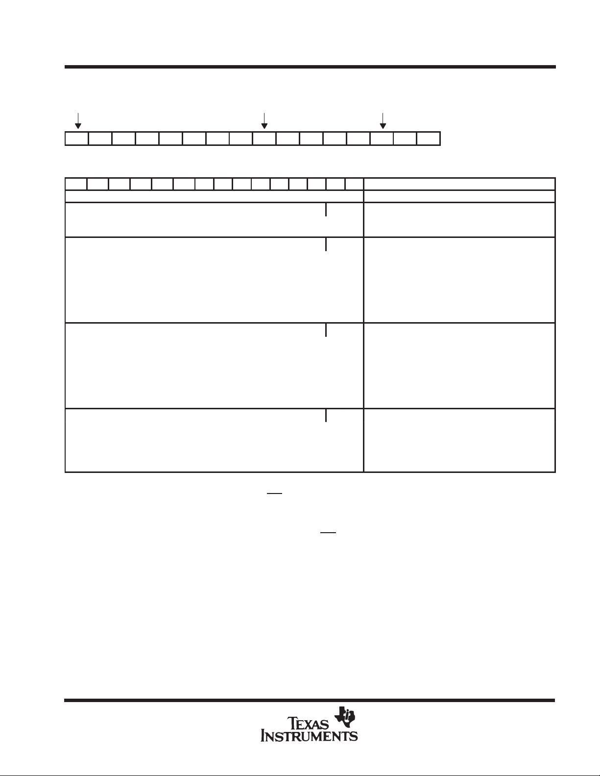
AIC DR or DX word bit pattern
A/D or D/A MSB,
1st bit sent 1st bit sent of 2nd byte A/D or D/A LSB
D14 D13 D12 D11 D10 D9 D8 D7 D6 D5 D4 D3 D2 D1 D0
D15
AIC DX data word format section
d15 d14 d13 d12 d11 d10 d9 d8 d7 d6 d5 d4 d2 d1 d0 COMMENTS
Primary DX serial communication protocol
← d15 (MSB) through d2 go to the D/A →
converter register
← d15 (MSB) through d2 go to the D/A →
converter register and RA + RA’ register values. The TX and RX Counter
← d15 (MSB) through d2 go to the D/A →
converter register and RA - RA’ register values. The TX and RX Counter
← d15 (MSB) through d2 go to the D/A →
converter register RA register values. The TX and RX Counter Bs are
NOTE: Setting the two least significant bits to 1 in the normal transmission of DAC information (Primary Communications) to the AIC will initiate
Secondary Communications upon completion of the Primary Communications.
Upon completion of the Primary Communication, FSX
Secondary Communication. The timing specifications for the Primary and Secondary Communications are identical. in this manner, the
Secondary Communication, if initiated, is interleaved between successive Primary Communications. This interleaving prevents the
Secondary Communication from interfering with the Primary Communications and DAC timing, thus preventing the AIC from skipping a
DAC output. It is important to note that in the synchronous mode, FSR
will remain high for four shift-clock cycles and will then go low and initiate the
0 0 The TX and RX Counter As are loaded with the TA and
RA register values. The TX and RX Counter Bs
areloaded with TB and RB register values.
0 1 The TX and Counter As are loaded with the TA + TA’
Bs are loaded with the TB and RB register values.
NOTE: d1 = 0, d0 = 1 will cause the next D/A and A/D
conversion periods to be changed by the addition of TA ’
and RA’ master clock cycles, in which TA’ and RA ’ can
be positive or negative or zero. Please refer to T able 1.
AIC Responses to Improper Conditions.
1 0 The TX and Counter As are loaded with the TA - TA’
Bs are loaded with the TB and RB register values.
NOTE: d1 = 0, d0 = 1 will cause the next D/A and A/D
conversion periods to be changed by the subtraction of
TA’ and RA’ Master Clock cycles, in which T A’ and RA
can be positive or negative or zero. Please refer to
Table 1. AIC Responses to Improper Conditions.
1 1 The TX and Counter As are loaded with the TA and
loaded with the TB and RB register values. After a
delay of four shift-clock cycles, a secondary
transmission will immediately follow to program the
AIC to operate in the desired configuration.
will not be asserted during Secondary Communications.
POST OFFICE BOX 655303 • DALLAS, TEXAS 75265
4–7
TLC32040M
ANALOG INTERFACE CIRCUIT
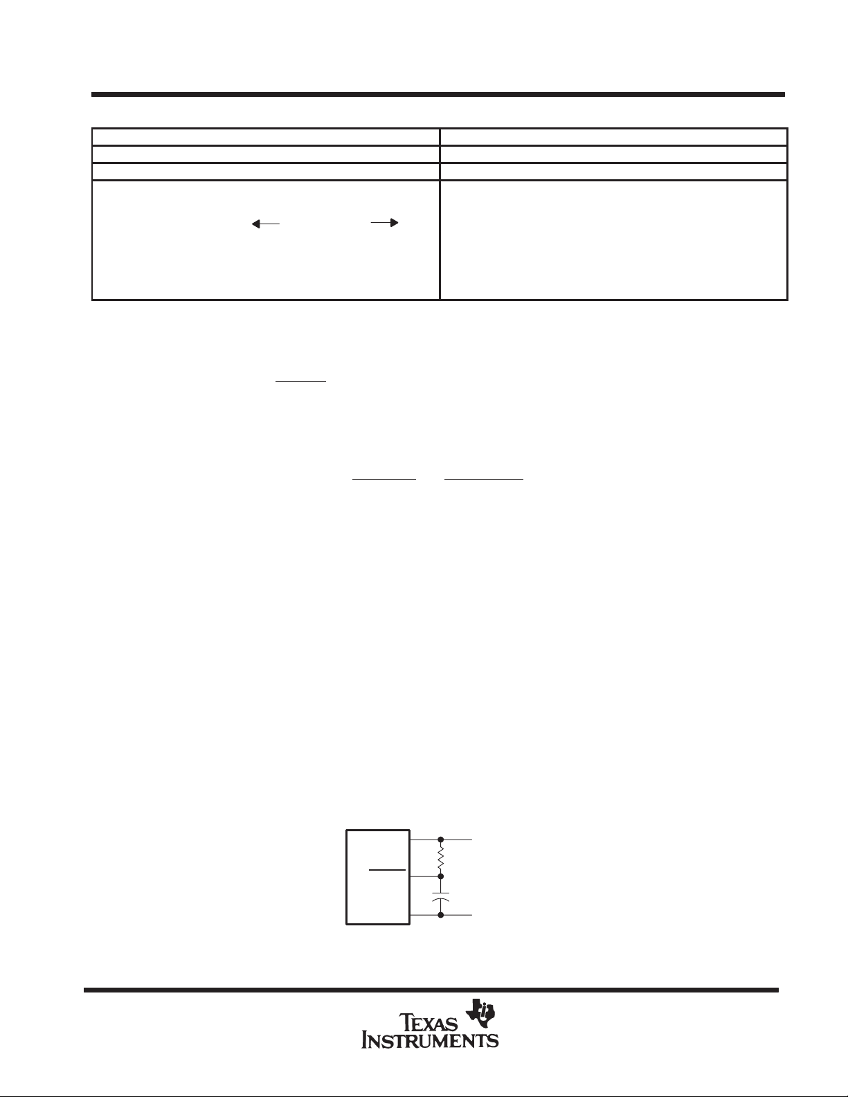
secondary DX serial communication protocol
x x | ← to TA register → | x x | ← to RA register → | 0 0 d13 and d6 are MSBs (unsigned binary)
x | ← to TA ’ register → | x | ← to RA’ register → | 0 1 d14 and d7 are 2s complement sign bits
x | ← to TB register → | x | ← to RB register → | 1 0 d14 and d7 are MSBs (unsigned binary)
x x x x x x x x d7 d6 d5 d4 d3 d2 1 1
d2 = 0/1 deletes/inserts the band-pass filter
||
Control Register
reset function
A reset function is provided to initiate serial communications between the AIC and DSP. The reset function will
initialize all AIC registers, including the control register. After power has been applied to the AIC, a
negative-going pulse on RESET
rate for a 5.184-MHz master clock input signal. The AIC, except the control register, will be initialized as follows
(see AIC DX data word format section):
will initialize the AIC registers to provide an 8-kHz A/D and D/A conversion
REGISTER
TA 9
TA’ 1
TB 24
RA 9
RA’ 1
RB 24
d3 = 0/1 disables/enables the loopback function
d4 = 0/1 disables/enables the AUX IN+ and AUX IN– terminals
d5 = 0/1 asynchronous/synchronous transmit and receive sections
d6 = 0/1 gain control bits (see gain control section)
d7 = 0/1 gain control bits (see gain control section)
INITIALIZED
REGISTER
VALUE (HEX)
The control register bits will be reset as follows (see AIC DX data word format section):
d7 = 1, d6 = 1, d5 = 1, d4 = 0, d3 = 0, d2 = 1
This initialization allows normal serial port communications to occur between the AIC and DSP. If the transmit
and receive sections are configured to operate synchronously and the user wishes to program different
conversion rates, only the T A, TA ’, and TB registers need to be programmed, since both transmit and receive
timing are synchronously derived from these registers (see the T erminal Functions table and AIC DX data word
format section).
The circuit shown below provides a reset on power up when power is applied in the sequence given under
power-up sequence. The circuit depends on the power supplies’ reaching their recommended values a
minimum of 800 ns before the capacitor charges to 0.8 V above DGTL GND.
V
CC+
RESET
V
CC–
5 V
200 kΩ
0.5 µF
–5 V
4–8
POST OFFICE BOX 655303 • DALLAS, TEXAS 75265
TLC32040M
ANALOG INTERFACE CIRCUIT
power-up sequence
To ensure proper operation of the AIC and as a safeguard against latch-up, it is recommended that a Schottky
diode with a forward voltage less than or equal to 0.4 V be connected from V
In the absence of such a diode, power should be applied in the following sequence: ANLG GND and DGTL GND,
V
CC–
, then V
and VDD. Also, no input signal should be applied until after power up.
CC+
AIC responses to improper conditions
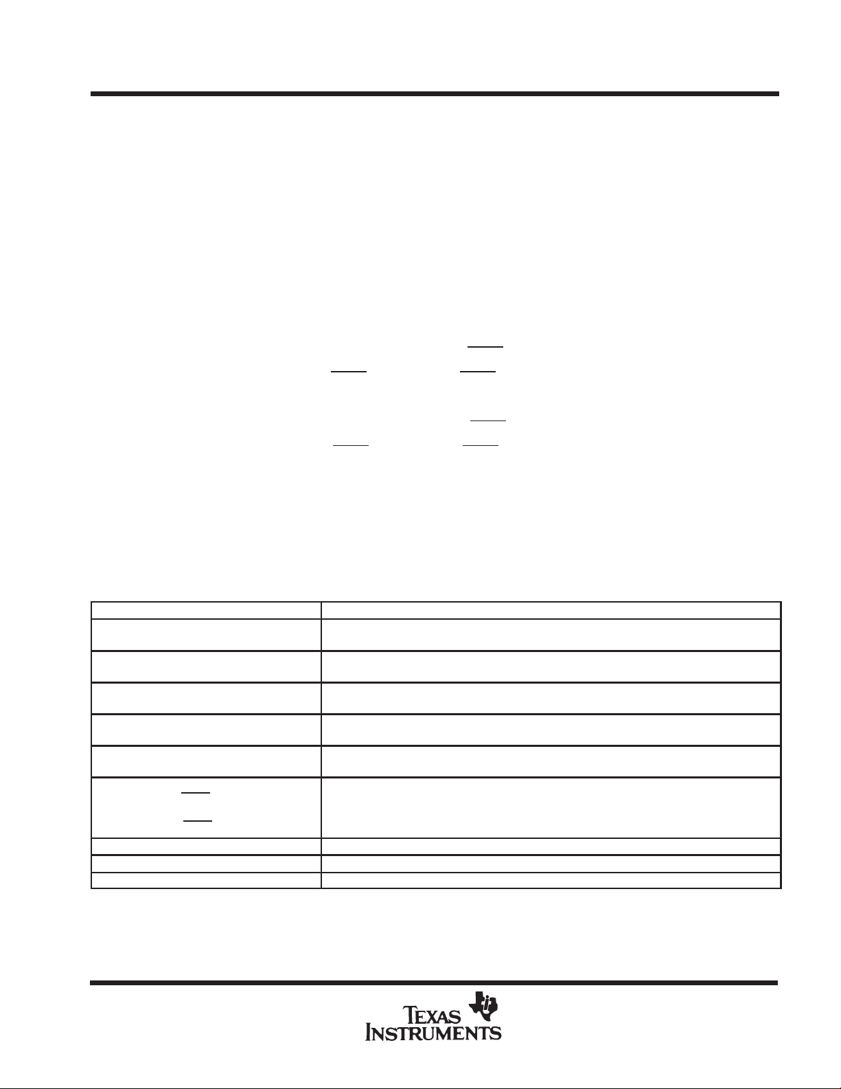
The AIC has provisions for responding to improper conditions. These improper conditions and the response of
the AIC to these conditions are presented in Table 1 below.
AIC register constraints
The following constraints are placed on the contents of the AIC registers:
to ANLG GND (see Figure 16).
CC–
1. TA register must be ≥ 4 in WORD mode (WORD/BYTE
2. TA register must be ≥ 5 in BYTE
mode (WORD/BYTE = low).
= high).
3. TA’ register can be either positive, negative, or zero.
4. RA register must be ≥ 4 in WORD mode (WORD/BYTE
5. RA register must be ≥ 5 in BYTE
mode (WORD/BYTE = low).
= high).
6. RA’ register can be either positive, negative, or zero.
7. (TA register ± TA’ register) must be > 1.
8. (RA register ± RA’ register) must be > 1.
9. TB register must be > 1.
Table 1. AIC Responses to Improper Conditions
IMPROPER CONDITION AIC RESPONSE
TA register + TA’ register = 0 or 1
TA register – TA’ register = 0 or 1
TA register + TA’ register < 0 MODULO 64 arithmetic is used to ensure that a positive value is loaded into the TX Counter A,
RA register + RA’ register = 0 or 1
RA register – RA’ register = 0 or 1
RA register + RA’ register = 0 or 1 MODULO 64 arithmetic is used to ensure that a positive value is loaded into the RX Counter
TA register = 0 or 1
RA register = 0 or 1
TA register < 4 in WORD mode
TA register < 5 in BYTE
RA register < 4 in WORD mode
RA register < 5 in BYTE
TB register = 0 or 1 Reprogram TB register with 24 HEX
RB register = 0 or 1 Reprogram TB register with 24 HEX
AIC and DSP cannot communicate Hold last DAC output
mode
mode
Reprogram TX Counter A with TA register value
i.e., TA register + TA’ register + 40 HEX is loaded into TX Counter A.
Reprogram RX Counter A with RA register value
A, i.e., RA register + RA’ register + 40 HEX is loaded into RX Counter A.
AIC is shutdown.
The AIC serial port no longer operates.
POST OFFICE BOX 655303 • DALLAS, TEXAS 75265
4–9
 Loading...