

Datasheet TLC2543MJB, TLC2543MJ, TLC2543IN, TLC2543IFNR, TLC2543IFN Datasheet (Texas Instruments)
...Page 1
TLC2543C, TLC2543I, TLC2543M
12-BIT ANALOG-TO-DIGITAL CONVERTERS
WITH SERIAL CONTROL AND 11 ANALOG INPUTS
SLAS079D – DECEMBER 1993 – REVISED MA Y 1997
1
POST OFFICE BOX 655303 • DALLAS, TEXAS 75265
D
12-Bit-Resolution A/D Converter
D
10-µs Conversion Time Over Operating
Temperature
D
11 Analog Input Channels
D
3 Built-In Self-Test Modes
D
Inherent Sample-and-Hold Function
D
Linearity Error...±1 LSB Max
D
On-Chip System Clock
D
End-of-Conversion Output
D
Unipolar or Bipolar Output Operation
(Signed Binary With Respect to 1/2 the
Applied Voltage Reference)
D
Programmable MSB or LSB First
D
Programmable Power Down
D
Programmable Output Data Length
D
CMOS Technology
D
Application Report Available
†
description
The TLC2543C and TLC2543I are 12-bit, switchedcapacitor, successive-approximation, analog-todigital converters. Each device has three control
inputs [chip select (CS
), the input-output clock (I/O
CLOCK), and the address input (DATA INPUT)] and
is designed for communication with the serial port of
a host processor or peripheral through a serial 3-state
output. The device allows high-speed data transfers
from the host.
In addition to the high-speed converter and versatile control capability, the device has an on-chip 14-channel
multiplexer that can select any one of 11 inputs or any one of three internal self-test voltages. The
sample-and-hold function is automatic. At the end of conversion, the end-of-conversion (EOC) output goes high
to indicate that conversion is complete. The converter incorporated in the device features differential
high-impedance reference inputs that facilitate ratiometric conversion, scaling, and isolation of analog circuitry
from logic and supply noise. A switched-capacitor design allows low-error conversion over the full operating
temperature range.
The TLC2543C is characterized for operation from T
A
= 0°C to 70°C. The TLC2543I is characterized for
operation from T
A
= –40°C to 85°C. The TLC2543M is characterized for operation from TA = –55°C to 125°C.
Copyright 1997, Texas Instruments Incorporated
PRODUCTION DATA information is current as of publication date.
Products conform to specifications per the terms of Texas Instruments
standard warranty. Production processing does not necessarily include
testing of all parameters.
Please be aware that an important notice concerning availability, standard warranty, and use in critical applications of
Texas Instruments semiconductor products and disclaimers thereto appears at the end of this data sheet.
†
Microcontroller Based Data Acquisition Using the TLC2543 12-bit Serial-Out ADC (SLAA012)
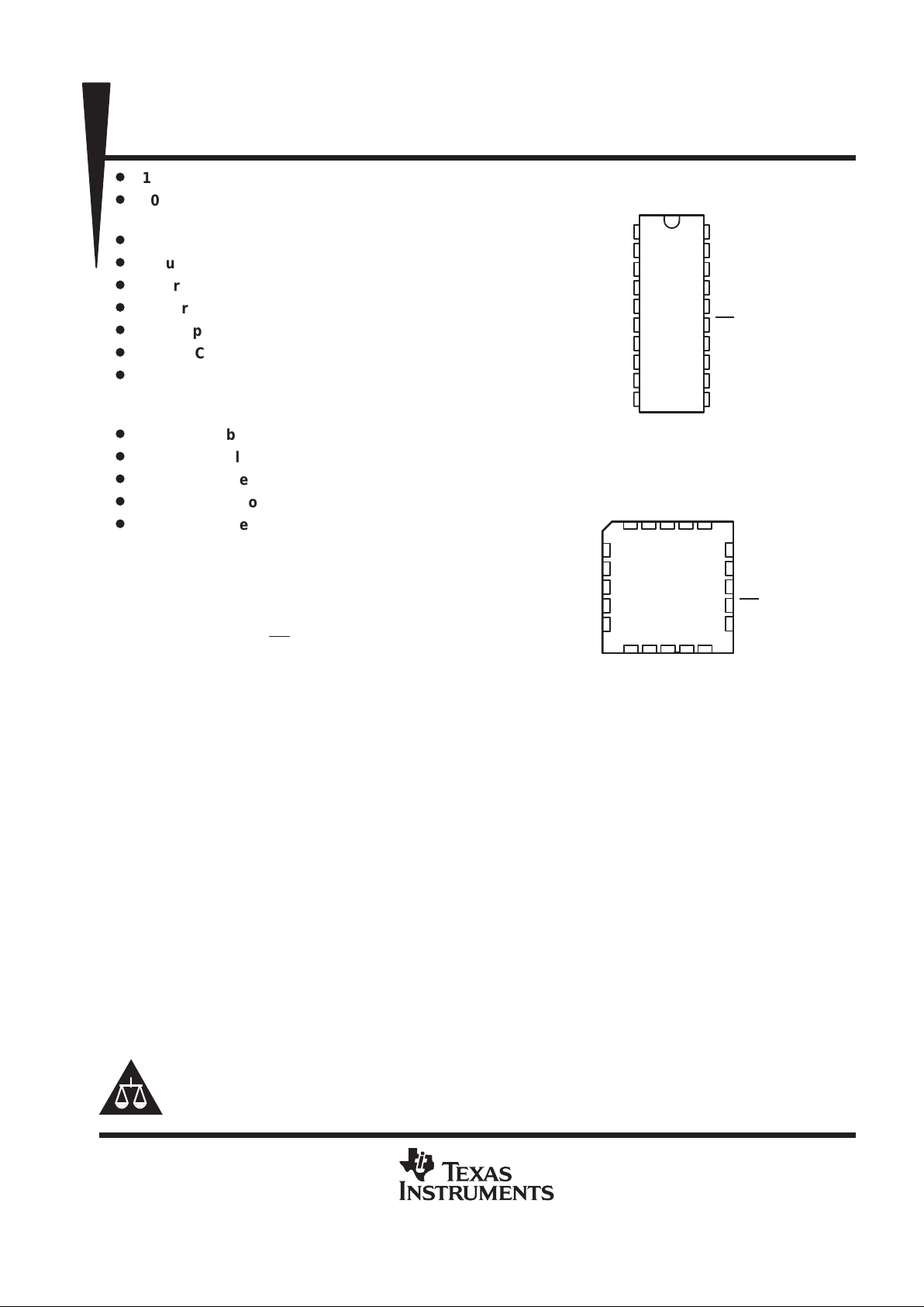
1
2
3
4
5
6
7
8
9
10
20
19
18
17
16
15
14
13
12
11
AIN0
AIN1
AIN2
AIN3
AIN4
AIN5
AIN6
AIN7
AIN8
GND
V
CC
EOC
I/O CLOCK
DATA INPUT
DATA OUT
CS
REF+
REF–
AIN10
AIN9
(TOP VIEW)
DB, DW, J, OR N PACKAGE
3 2 1 20 19
910111213
4
5
6
7
8
18
17
16
15
14
I/O CLOCK
DATA INPUT
DATA OUT
CS
AIN3
AIN4
AIN5
AIN6
AIN7
FK OR FN PACKAGE
(TOP VIEW)
AIN1
AIN0
AIN10
REF –
AIN2
EOC
AIN8
GND
AIN9
V
CC
REF+
Page 2
TLC2543C, TLC2543I, TLC2543M
12-BIT ANALOG-TO-DIGITAL CONVERTERS
WITH SERIAL CONTROL AND 11 ANALOG INPUTS
SLAS079D – DECEMBER 1993 – REVISED MA Y 1997
2
POST OFFICE BOX 655303 • DALLAS, TEXAS 75265
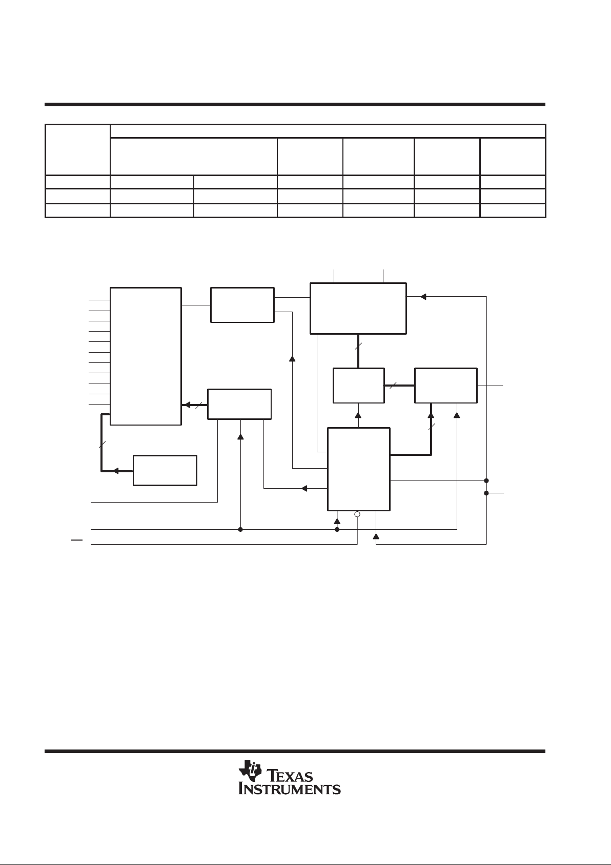
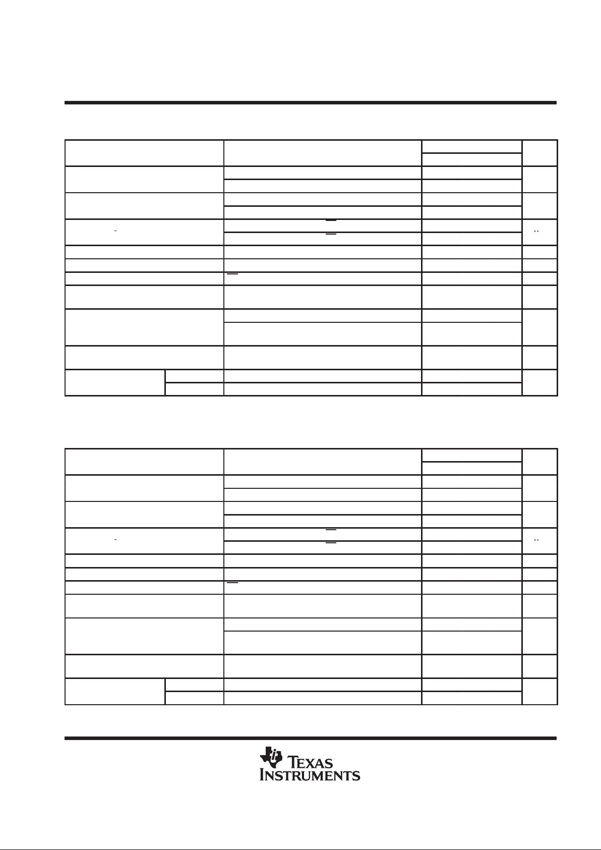
AVAILABLE OPTIONS
PACKAGE
T
A
SMALL OUTLINE
PLASTIC CHIP
CARRIER
PLASTIC CHIP
CARRIER
PLASTIC DIP PLASTIC DIP
(DB)
†
(DW)
†
(FK) (FN)
†
(J) (N)
0°C to 70°C TLC2543CDB TLC2543CDW — TLC2543CFN — TLC2543CN
–40°C to 85°C — TLC2543IDW — TLC2543IFN — TLC2543IN
–55°C to 125°C — — TLC2543MFK — TLC2543MJ —
†
Available in tape and reel and ordered as the TLC2543CDBLE, TLC2543CDWR, TLC2543IDWR, TLC2543CFNR, or TLC2543IFNR.
functional block diagram
14-Channel
Analog
Multiplexer
Sample-and-
Hold
Function
12-Bit
Analog-to-Digital
Converter
(Switched Capacitors)
Self-Test
Reference
Output
Data
Register
12-to-1 Data
Selector and
Driver
Control Logic
and I/O
Counters
Input Address
Register
4
12
12
4
REF+ REF–
DATA
OUT
DATA
INPUT
I/O CLOCK
CS
3
EOC
17
18
15
AIN0
AIN1
AIN2
AIN3
AIN4
AIN5
AIN6
AIN7
AIN8
AIN9
AIN10
1
2
3
4
5
6
7
8
9
11
12
14 13
16
19
Page 3
TLC2543C, TLC2543I, TLC2543M
12-BIT ANALOG-TO-DIGITAL CONVERTERS
WITH SERIAL CONTROL AND 11 ANALOG INPUTS
SLAS079D – DECEMBER 1993 – REVISED MA Y 1997
3
POST OFFICE BOX 655303 • DALLAS, TEXAS 75265
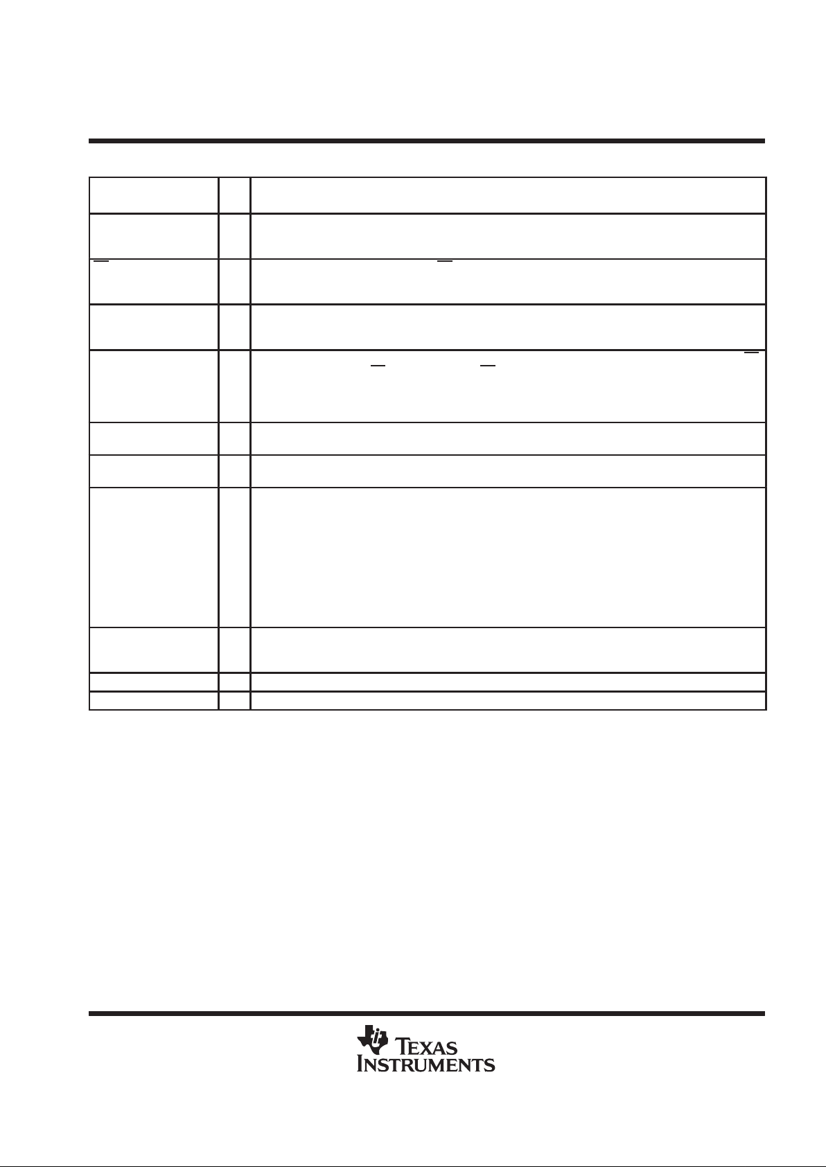
Terminal Functions
TERMINAL
NAME NO.
I/O
DESCRIPTION
AIN0 – AIN10 1–9,
11, 12
I Analog input. These 1 1 analog-signal inputs are internally multiplexed. The driving source impedance should
be less than or equal to 50 Ω for 4.1-MHz I/O CLOCK operation and be capable of slewing the analog input
voltage into a capacitance of 60 pF.
CS 15 I Chip select. A high-to-low transition on CS resets the internal counters and controls and enables DAT A OUT,
DAT A INPUT, and I/O CLOCK. A low-to-high transition disables DAT A INPUT and I/O CLOCK within a setup
time.
DATA INPUT 17 I Serial-data input. A 4-bit serial address selects the desired analog input or test voltage to be converted next.
The serial data is presented with the MSB first and is shifted in on the first four rising edges of I/O CLOCK.
After the four address bits are read into the address register, I/O CLOCK clocks the remaining bits in order.
DATA OUT 16 O The 3-state serial output for the A/D conversion result. DATA OUT is in the high-impedance state when CS
is high and active when CS is low. With a valid CS, DATA OUT is removed from the high-impedance state
and is driven to the logic level corresponding to the MSB/LSB† value of the previous conversion result. The
next falling edge of I/O CLOCK drives DAT A OUT to the logic level corresponding to the next MSB/LSB, and
the remaining bits are shifted out in order.
EOC 19 O End of conversion. EOC goes from a high to a low logic level after the falling edge of the last I/O CLOCK and
remains low until the conversion is complete and the data is ready for transfer.
GND 10 Ground. GND is the ground return terminal for the internal circuitry. Unless otherwise noted, all voltage
measurements are with respect to GND.
I/O CLOCK 18 I Input/output clock. I/O CLOCK receives the serial input and performs the following four functions:
1. It clocks the eight input data bits into the input data register on the first eight rising edges of I/O CLOCK
with the multiplexer address available after the fourth rising edge.
2. On the fourth falling edge of I/O CLOCK, the analog input voltage on the selected multiplexer input
begins charging the capacitor array and continues to do so until the last falling edge of the I/O
CLOCK.
3. It shifts the 11 remaining bits of the previous conversion data out on DATA OUT. Data changes on
the falling edge of I/O CLOCK.
4. It transfers control of the conversion to the internal state controller on the falling edge of the last
I/O CLOCK.
REF+ 14 I Positive reference voltage The upper reference voltage value (nominally VCC) is applied to REF+. The
maximum input voltage range is determined by the difference between the voltage applied to this terminal and
the voltage applied to the REF– terminal.
REF– 13 I Negative reference voltage. The lower reference voltage value (nominally ground) is applied to REF–.
V
CC
20 Positive supply voltage
†
MSB/LSB = Most significant bit /least significant bit
Page 4
TLC2543C, TLC2543I, TLC2543M
12-BIT ANALOG-TO-DIGITAL CONVERTERS
WITH SERIAL CONTROL AND 11 ANALOG INPUTS
SLAS079D – DECEMBER 1993 – REVISED MA Y 1997
4
POST OFFICE BOX 655303 • DALLAS, TEXAS 75265
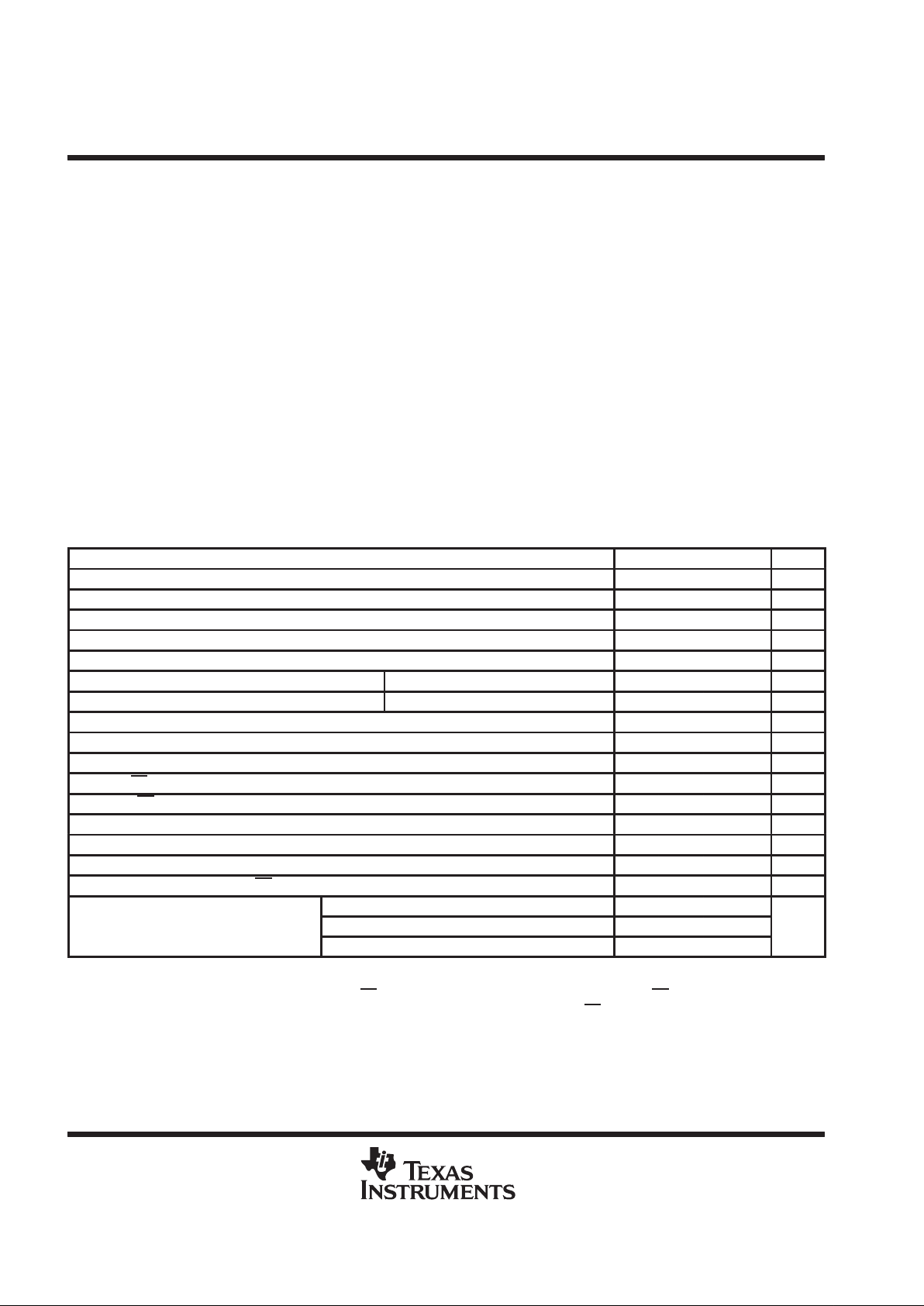
absolute maximum ratings over operating free-air temperature range (unless otherwise
noted)
†
Supply voltage range, V
CC
(see Note 1) –0.5 V to 6.5 V. . . . . . . . . . . . . . . . . . . . . . . . . . . . . . . . . . . . . . . . . . . . .
Input voltage range, V
I
(any input) –0.3 V to VCC + 0.3 V. . . . . . . . . . . . . . . . . . . . . . . . . . . . . . . . . . . . . . . . . . . .
Output voltage range, V
O
–0.3 V to VCC + 0.3 V. . . . . . . . . . . . . . . . . . . . . . . . . . . . . . . . . . . . . . . . . . . . . . . . . . .
Positive reference voltage, V
ref+
V
CC
+ 0.1 V. . . . . . . . . . . . . . . . . . . . . . . . . . . . . . . . . . . . . . . . . . . . . . . . . . . . . .
Negative reference voltage, V
ref–
–0.1 V. . . . . . . . . . . . . . . . . . . . . . . . . . . . . . . . . . . . . . . . . . . . . . . . . . . . . . . . . .
Peak input current, I
I
(any input) ±20 mA. . . . . . . . . . . . . . . . . . . . . . . . . . . . . . . . . . . . . . . . . . . . . . . . . . . . . . . . . .
Peak total input current, I
I
(all inputs) ±30 mA. . . . . . . . . . . . . . . . . . . . . . . . . . . . . . . . . . . . . . . . . . . . . . . . . . . . . .
Operating free-air temperature range, T
A
: TLC2543C 0°C to 70°C. . . . . . . . . . . . . . . . . . . . . . . . . . . . . . . . . . .
TLC2543I –40°C to 85°C. . . . . . . . . . . . . . . . . . . . . . . . . . . . . . . . .
TLC2543M –55°C to 125°C. . . . . . . . . . . . . . . . . . . . . . . . . . . . . . .
Storage temperature range, T
stg
–65°C to 150°C. . . . . . . . . . . . . . . . . . . . . . . . . . . . . . . . . . . . . . . . . . . . . . . . . . .
Lead temperature 1,6 mm (1/16 inch) from the case for 10 seconds 260°C. . . . . . . . . . . . . . . . . . . . . . . . . . . .
†
Stresses beyond those listed under “absolute maximum ratings” may cause permanent damage to the device. These are stress ratings only, and
functional operation of the device at these or any other conditions beyond those indicated under “recommended operating conditions” is not
implied. Exposure to absolute-maximum-rated conditions for extended periods may affect device reliability.
NOTE 1: All voltage values are with respect to the GND terminal with REF– and GND wired together (unless otherwise noted).
recommended operating conditions
MIN NOM MAX UNIT
Supply voltage, V
CC
4.5 5 5.5 V
Positive reference voltage, V
ref+
(see Note 2) V
CC
V
Negative reference voltage, V
ref–
(see Note 2) 0 V
Differential reference voltage, V
ref+
– V
ref–
(see Note 2) 2.5 VCCVCC+0.1 V
Analog input voltage (see Note 2) 0 V
CC
V
High-level control input voltage, V
IH
VCC = 4.5 V to 5.5 V 2 V
Low-level control input voltage, V
IL
VCC = 4.5 V to 5.5 V 0.8 V
Clock frequency at I/O CLOCK 0 4.1 MHz
Setup time, address bits at DATA INPUT before I/O CLOCK↑, t
su(A)
(see Figure 4) 100 ns
Hold time, address bits after I/O CLOCK↑, t
h(A)
(see Figure 4) 0 ns
Hold time, CS low after last I/O CLOCK↓, t
h(CS)
(see Figure 5) 0 ns
Setup time, CS low before clocking in first address bit, t
su(CS)
(see Note 3 and Figure 5) 1.425 µs
Pulse duration, I/O CLOCK high, t
wH(I/O)
120 ns
Pulse duration, I/O CLOCK low, t
wL(I/O)
120 ns
Transition time, I/O CLOCK high to low , t
t(I/O)
(see Note 4 and Figure 6) 1 µs
Transition time, DATA INPUT and CS, t
t(CS)
10 µs
TLC2543C 0 70
Operating free-air temperature, T
A
TLC2543I –40 85
°C
TLC2543M –55 125
NOTES: 2. Analog input voltages greater than that applied to REF+ convert as all ones (111111111111), while input voltages less than that applied
to REF– convert as all zeros (000000000000).
3. T o minimize errors caused by noise at the CS
input, the internal circuitry waits for a setup time after CS↓ before responding to control
input signals. No attempt should be made to clock in an address until the minimum CS
setup time has elapsed.
4. This is the time required for the clock input signal to fall from VIHmin to VILmax or to rise from VILmax to VIHmin. In the vicinity of
normal room temperature, the devices function with input clock transition time as slow as 1 µs for remote data acquisition applications
where the sensor and the A/D converter are placed several feet away from the controlling microprocessor.
Page 5
TLC2543C, TLC2543I, TLC2543M
12-BIT ANALOG-TO-DIGITAL CONVERTERS
WITH SERIAL CONTROL AND 11 ANALOG INPUTS
SLAS079D – DECEMBER 1993 – REVISED MA Y 1997
5
POST OFFICE BOX 655303 • DALLAS, TEXAS 75265
electrical characteristics over recommended operating free-air temperature range,
V
CC
= V
ref+
= 4.5 V to 5.5 V, f
(I/O CLOCK)
= 4.1 MHz (unless otherwise noted)
TLC2543C, TLC2543I
PARAMETER
TEST CONDITIONS
MIN TYP†MAX
UNIT
p
VCC = 4.5 V, IOH = –1.6 mA 2.4
VOHHigh-level output voltage
VCC = 4.5 V to 5.5 V, IOH = –20 µA VCC–0.1
V
p
VCC = 4.5 V, IOL = 1.6 mA 0.4
VOLLow-level output voltage
VCC = 4.5 V to 5.5 V, IOL = 20 µA 0.1
V
High-impedance off-state output
VO = VCC, CS at V
CC
1 2.5
I
OZ
g
current
VO = 0,
CS at V
CC
1 –2.5
µ
A
I
IH
High-level input current VI = V
CC
1 2.5 µA
I
IL
Low-level input current VI = 0 1 –2.5 µA
I
CC
Operating supply current CS at 0 V 1 2.5 mA
I
CC(PD)
Power-down current
For all digital inputs,
0 ≤ VI ≤ 0.5 V or VI ≥ VCC – 0.5 V
4 25 µA
Selected channel at VCC, Unselected channel at 0 V 1
Selected channel leakage
current
Selected channel at 0 V ,
Unselected channel at V
CC
–1
µA
Maximum static analog
reference current into REF+
V
ref+
= VCC, V
ref–
= GND 1 2.5 µA
Input
Analog inputs 30 60
p
C
i
capacitance
Control inputs 5 15
pF
†
All typical values are at VCC = 5 V, TA = 25°C.
electrical characteristics over recommended operating free-air temperature range,
V
CC
= V
ref+
= 4.5 V to 5.5 V, f
(I/O CLOCK)
= 4.1 MHz (unless otherwise noted)
TLC2543M
PARAMETER
TEST CONDITIONS
MIN TYP†MAX
UNIT
p
VCC = 4.5 V, IOH = –1.6 mA 2.4
VOHHigh-level output voltage
VCC = 4.5 V to 5.5 V, IOH = –20 µA VCC–0.1
V
p
VCC = 4.5 V, IOL = 1.6 mA 0.4
VOLLow-level output voltage
VCC = 4.5 V to 5.5 V, IOL = 20 µA 0.1
V
High-impedance off-state output
VO = VCC, CS at V
CC
1 2.5
I
OZ
g
current
VO = 0,
CS at V
CC
1 –2.5
µ
A
I
IH
High-level input current VI = V
CC
1 10 µA
I
IL
Low-level input current VI = 0 1 –10 µA
I
CC
Operating supply current CS at 0 V 1 10 mA
I
CC(PD)
Power-down current
For all digital inputs,
0 ≤ VI ≤ 0.5 V or VI ≥ VCC – 0.5 V
4 25 µA
Selected channel at VCC, Unselected channel at 0 V 10
Selected channel leakage
current
Selected channel at 0 V ,
Unselected channel at V
CC
–10
µA
Maximum static analog
reference current into REF+
V
ref+
= VCC, V
ref–
= GND 1 2.5 µA
Input
Analog inputs 30 60
p
C
i
capacitance
Control inputs 5 15
pF
†
All typical values are at VCC = 5 V, TA = 25°C.
Page 6
TLC2543C, TLC2543I, TLC2543M
12-BIT ANALOG-TO-DIGITAL CONVERTERS
WITH SERIAL CONTROL AND 11 ANALOG INPUTS
SLAS079D – DECEMBER 1993 – REVISED MA Y 1997
6
POST OFFICE BOX 655303 • DALLAS, TEXAS 75265
operating characteristics over recommended operating free-air temperature range,
V
CC
= V
ref+
= 4.5 V to 5.5 V, f
(I/O CLOCK)
= 4.1 MHz
PARAMETER TEST CONDITIONS MIN TYP
†
MAX UNIT
E
L
Linearity error (see Note 5) See Figure 2 ±1 LSB
E
D
Differential linearity error See Figure 2 ±1 LSB
E
O
Offset error (see Note 6)
See Note 2 and
Figure 2
±1.5 LSB
E
G
Gain error (see Note 6)
See Note 2 and
Figure 2
±1 LSB
E
T
Total unadjusted error (see Note 7) ±1.75 LSB
DATA INPUT = 1011 2048
Self-test output code (see Table 3 and Note 8)
DATA INPUT = 1100 0
DATA INPUT = 1101 4095
t
conv
Conversion time See Figures 9–14 8 10 µs
t
c
Total cycle time (access, sample, and conversion)
See Figures 9–14
and Note 9
10 + total
I/O CLOCK
periods +
t
d(I/O-EOC)
µs
t
acq
Channel acquisition time (sample)
See Figures 9–14
and Note 9
4 12
I/O
CLOCK
periods
t
v
Valid time, DATA OUT remains valid after I/O CLOCK↓ See Figure 6 10 ns
t
d(I/O-DATA)
Delay time, I/O CLOCK↓ to DATA OUT valid See Figure 6 150 ns
t
d(I/O-EOC)
Delay time, last I/O CLOCK↓ to EOC↓ See Figure 7 1.5 2.2 µs
t
d(EOC-DATA)
Delay time, EOC↑ to DATA OUT (MSB/LSB) See Figure 8 100 ns
t
PZH
, t
PZL
Enable time, CS↓ to DATA OUT (MSB/LSB driven) See Figure 3 0.7 1.3 µs
t
PHZ
, t
PLZ
Disable time, CS↑ to DATA OUT (high impedance) See Figure 3 70 150 ns
t
r(EOC)
Rise time, EOC See Figure 8 15 50 ns
t
f(EOC)
Fall time, EOC See Figure 7 15 50 ns
t
r(bus)
Rise time, data bus See Figure 6 15 50 ns
t
f(bus)
Fall time, data bus See Figure 6 15 50 ns
t
d(I/O-CS)
Delay time, last I/O CLOCK↓ to CS↓ to abort conversion
(see Note 10)
5 µs
†
All typical values are at TA = 25°C.
NOTES: 2. Analog input voltages greater than that applied to REF + convert as all ones (111111111111), while input voltages less than that
applied to REF– convert as all zeros (000000000000).
5. Linearity error is the maximum deviation from the best straight line through the A/D transfer characteristics.
6. Gain error is the difference between the actual midstep value and the nominal midstep value in the transfer diagram at the specified
gain point after the offset error has been adjusted to zero. Offset error is the difference between the actual midstep value an d the
nominal midstep value at the offset point.
7. Total unadjusted error comprises linearity, zero-scale, and full-scale errors.
8. Both the input address and the output codes are expressed in positive logic.
9. I/O CLOCK period = 1/(I/O CLOCK frequency) (see Figure 7).
10. Any transitions of CS
are recognized as valid only when the level is maintained for a setup time. CS must be taken low at ≤ 5 µs
of the tenth I/O CLOCK falling edge to ensure a conversion is aborted. Between 5 µs and 10 µs, the result is uncertain as to whether
the conversion is aborted or the conversion results are valid.
Page 7
TLC2543C, TLC2543I, TLC2543M
12-BIT ANALOG-TO-DIGITAL CONVERTERS
WITH SERIAL CONTROL AND 11 ANALOG INPUTS
SLAS079D – DECEMBER 1993 – REVISED MA Y 1997
7
POST OFFICE BOX 655303 • DALLAS, TEXAS 75265
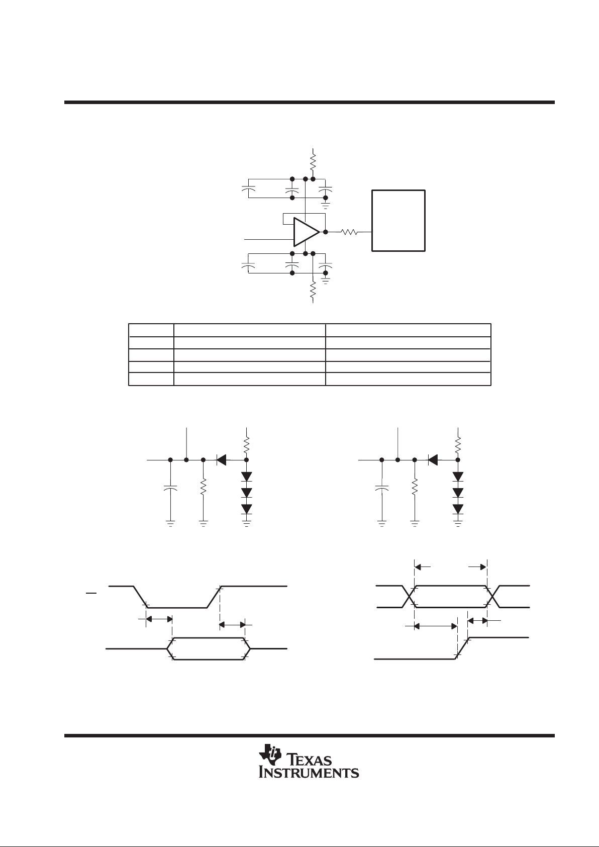
PARAMETER MEASUREMENT INFORMATION
_
+
C2
0.1 µF
C1
10 µF
C3
470 pF
50 Ω
15 V
50 Ω
–15 V
V
I
AIN0–AIN10
TLC2543
10 Ω
U1
C1
10 µF
C3
470 pF
C2
0.1 µF
LOCATION
U1
C1
C2
C3
DESCRIPTION
OP27
10-µF 35-V tantalum capacitor
0.1-µF ceramic NPO SMD capacitor
470-pF porcelain Hi-Q SMD capacitor
PART NUMBER
—
—
AVX 12105C104KA105 or equivalent
Johanson 201S420471JG4L or equivalent
Figure 1. Analog Input Buffer to Analog Inputs AIN0–AIN10
EOC
CL = 50 pF
12 kΩ
DATA OUT
Test Point
V
CC
RL = 2.18 kΩ
CL = 100 pF
12 kΩ
Test Point
V
CC
RL = 2.18 kΩ
Figure 2. Load Circuits
CS
DATA
OUT
2.4 V
0.4 V
90%
10%
t
PZH
, t
PZL
t
PHZ
, t
PLZ
0.8 V
2 V
Figure 3. DATA OUT to Hi-Z Voltage Waveforms
DATA INPUT
t
h(A)
0.8 V
2 V
I/O CLOCK
Data
Valid
t
su(A)
0.8 V
Figure 4. DATA INPUT and I/O CLOCK
Voltage Waveforms
Page 8
TLC2543C, TLC2543I, TLC2543M
12-BIT ANALOG-TO-DIGITAL CONVERTERS
WITH SERIAL CONTROL AND 11 ANALOG INPUTS
SLAS079D – DECEMBER 1993 – REVISED MA Y 1997
8
POST OFFICE BOX 655303 • DALLAS, TEXAS 75265
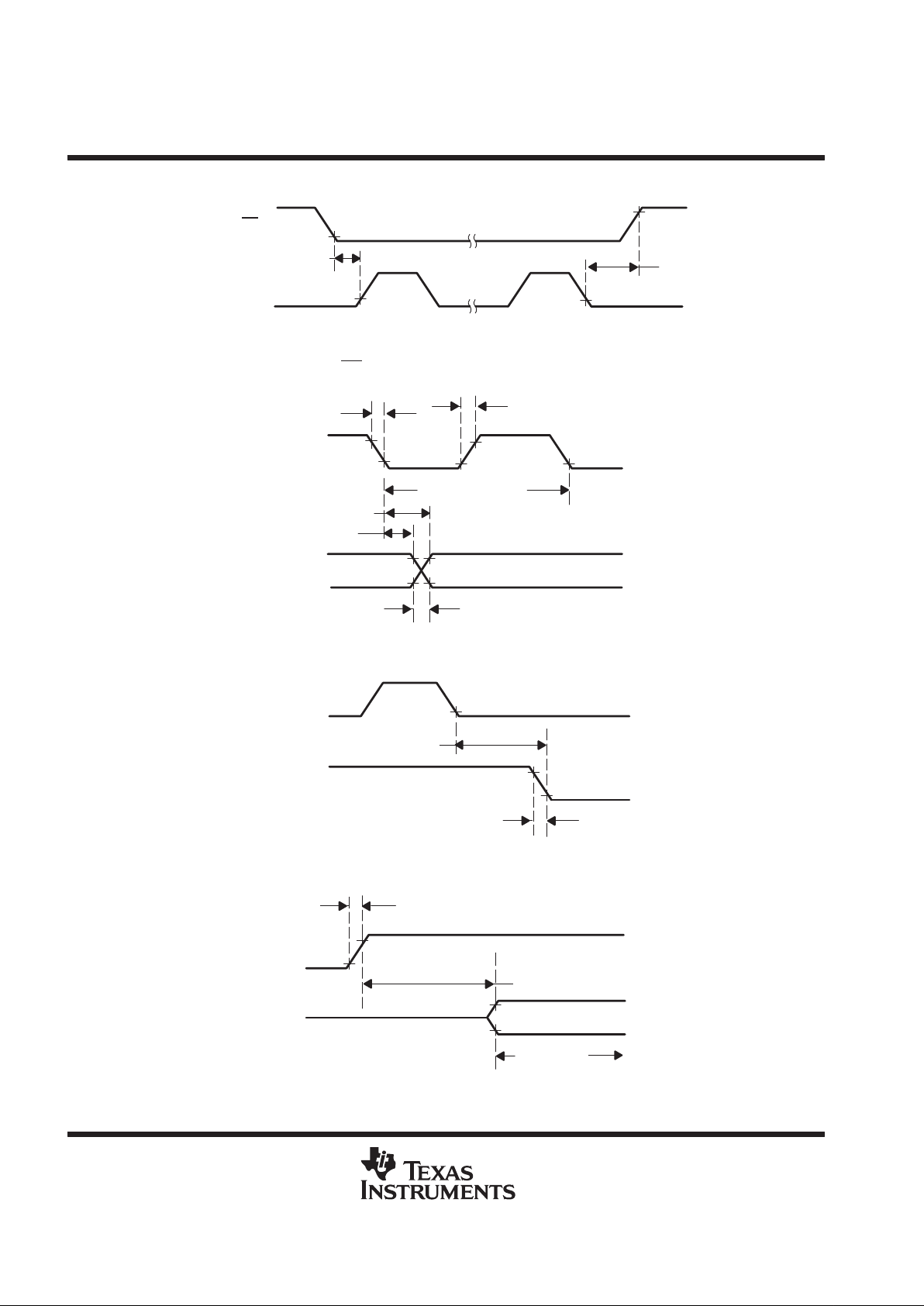
PARAMETER MEASUREMENT INFORMATION
Last
Clock
CS
0.8 V
2 V
0.8 V
t
su(CS)
0.8 V
I/O CLOCK
t
h(CS)
NOTE A: T o ensure full conversion accuracy, it is recommended that no input signal change
occurs while a conversion is ongoing.
Figure 5. CS and I/O CLOCK Voltage Waveforms
0.4 V
2.4 V
0.4 V
2.4 V
2 V
0.8 V
I/O CLOCK
DATA OUT
t
t(I/O)
0.8 V
2 V
t
r(bus)
, t
f(bus)
t
d(I/O-DATA)
t
v
t
t(I/O)
0.8 V
I/O CLOCK Period
Figure 6. I/O CLOCK and DATA OUT Voltage Waveforms
Last
Clock
0.8 V
2.4 V
0.4 V
t
f(EOC)
t
d(I/O-EOC)
I/O CLOCK
EOC
Figure 7. I/O CLOCK and EOC Voltage Waveforms
0.4 V
2.4 V
EOC
t
d(EOC-DATA)
Valid MSB
DATA OUT
0.4 V
2.4 V
t
r(EOC)
Figure 8. EOC and DATA OUT Voltage Waveforms
Page 9
TLC2543C, TLC2543I, TLC2543M
12-BIT ANALOG-TO-DIGITAL CONVERTERS
WITH SERIAL CONTROL AND 11 ANALOG INPUTS
SLAS079D – DECEMBER 1993 – REVISED MA Y 1997
9
POST OFFICE BOX 655303 • DALLAS, TEXAS 75265
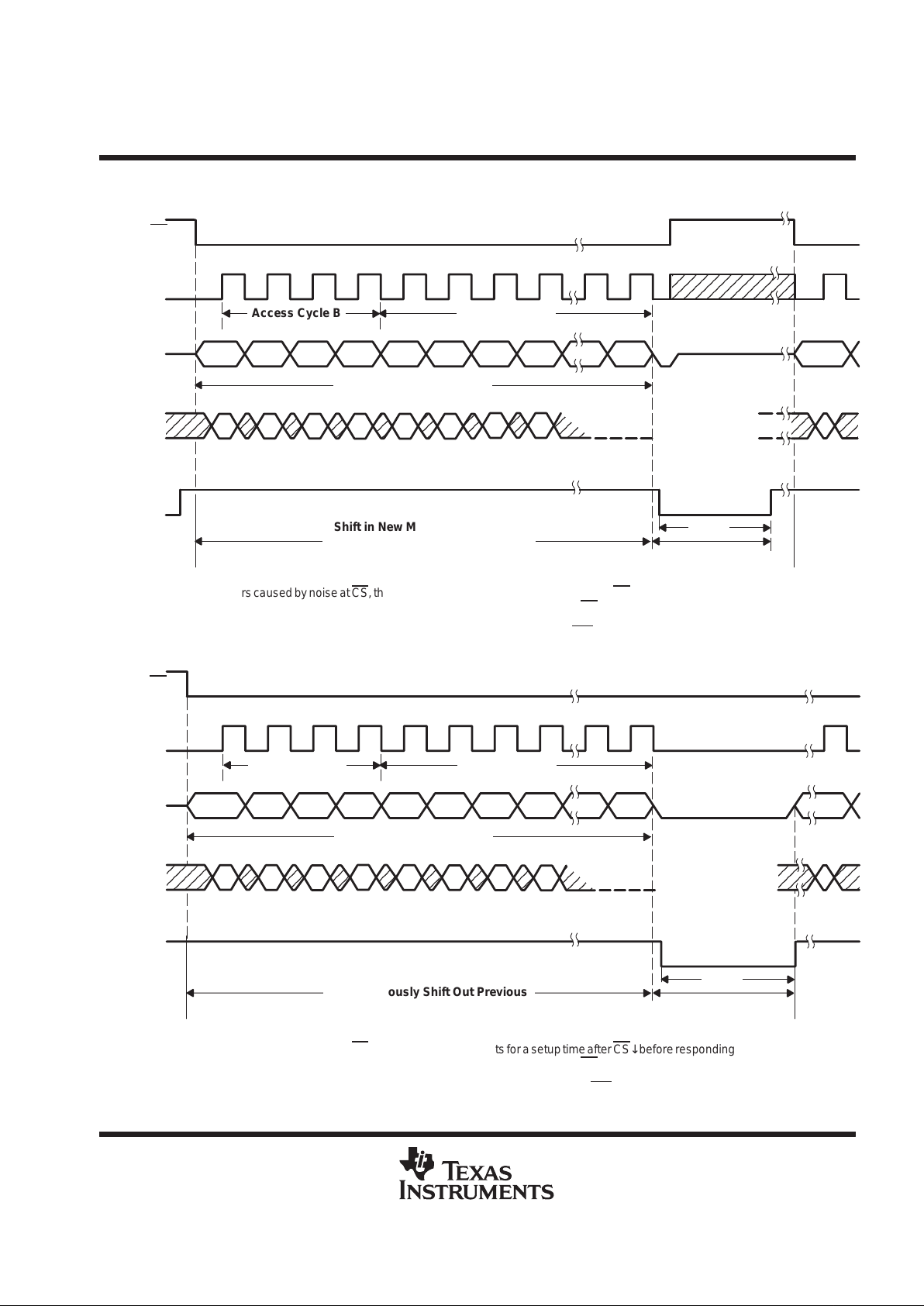
PARAMETER MEASUREMENT INFORMATION
ÎÎ
Access Cycle B
Shift in New Multiplexer Address,
Simultaneously Shift Out Previous
Conversion Value
Sample Cycle B
A/D Conversion
Interval
InitializeInitialize
MSB LSB
Previous Conversion Data
MSB LSB
B7 B6 B5 B4
C7
B11A11 A10 A9 A8 A7 A6 A5 A4 A1 A0
Hi-Z State
1 2 3 4 5 6 7 8 11 12 1
I/O
CLOCK
DATA
OUT
DATA
INPUT
CS
EOC
(see Note A)
B3 B2 B1 B0
Î
t
conv
NOTE A: To minimize errors caused by noise at CS
, the internal circuitry waits for a setup time after CS↓ before responding to control input signals.
Therefore, no attempt should be made to clock in an address until the minimum CS
setup time has elapsed.
Figure 9. Timing for 12-Clock Transfer Using CS With MSB First
ÎÎ
ÎÎ
Access Cycle B
Shift in New Multiplexer Address,
Simultaneously Shift Out Previous
Conversion Value
Sample Cycle B
A/D Conversion
Interval
Initialize
MSB LSB
Previous Conversion Data
MSB LSB
B7 B6 B5 B4 C7
B11A11 A10 A9 A8 A7 A6 A5 A4 A1 A0
Low Level
1 2 3 4 5 6 7 8 11 12 1
I/O
CLOCK
DATA
OUT
DATA
INPUT
CS
EOC
Initialize
(see Note A)
B3 B2 B1 B0
t
conv
NOTE A: To minimize errors caused by noise at CS
, the internal circuitry waits for a setup time after CS↓ before responding to control input signals.
Therefore, no attempt should be made to clock in an address until the minimum CS
setup time has elapsed.
Figure 10. Timing for 12-Clock Transfer Not Using CS With MSB First
Page 10

TLC2543C, TLC2543I, TLC2543M
12-BIT ANALOG-TO-DIGITAL CONVERTERS
WITH SERIAL CONTROL AND 11 ANALOG INPUTS
SLAS079D – DECEMBER 1993 – REVISED MA Y 1997
10
POST OFFICE BOX 655303 • DALLAS, TEXAS 75265
PARAMETER MEASUREMENT INFORMATION
ÎÎ
Access Cycle B
Shift in New Multiplexer Address,
Simultaneously Shift Out Previous
Conversion Value
Sample Cycle B
A/D Conversion
Interval
Initialize
MSB LSB
Previous Conversion Data
MSB LSB
B7 B6 B5 B4 C7
B7A7 A6 A5 A4 A3 A2 A1 A0
12345678 1
I/O CLOCK
DATA OUT
DATA INPUT
CS
EOC
Initialize
Hi-Z
(see Note A)
B3 B2 B1 B0
Î
t
conv
NOTE A: To minimize errors caused by noise at CS, the internal circuitry waits for a setup time after CS↓ before responding to control input signals.
Therefore, no attempt should be made to clock in an address until the minimum CS
setup time has elapsed.
Figure 11. Timing for 8-Clock Transfer Using CS With MSB First
Access Cycle B Sample Cycle B
A/D Conversion
Interval
Initialize
MSB LSB
Previous Conversion Data
MSB LSB
B7 B6 B5 B4 C7
B7A7 A6 A5 A4 A3 A2 A1 A0
Low Level
123456 78 1
I/O CLOCK
DATA OUT
DATA INPUT
CS
EOC
Initialize
(see Note A)
B3 B2 B1 B0
Î
t
conv
Shift in New Multiplexer Address,
Simultaneously Shift Out Previous
Conversion Value
NOTE A: To minimize errors caused by noise at CS
, the internal circuitry waits for a setup time after CS↓ before responding to control input signals.
Therefore, no attempt should be made to clock in an address until the minimum CS
setup time has elapsed.
Figure 12. Timing for 8-Clock Transfer Not Using CS With MSB First
Page 11

TLC2543C, TLC2543I, TLC2543M
12-BIT ANALOG-TO-DIGITAL CONVERTERS
WITH SERIAL CONTROL AND 11 ANALOG INPUTS
SLAS079D – DECEMBER 1993 – REVISED MA Y 1997
11
POST OFFICE BOX 655303 • DALLAS, TEXAS 75265
PARAMETER MEASUREMENT INFORMATION
A/D Conversion
Interval
Initialize
MSB LSB
MSB LSB
B7 B6 B5 B4 C7
B15A15 A14 A13 A12 A11 A10 A9 A8 A1 A0
1 2 3 4 5 6 7 8 15 16 1
I/O
CLOCK
DATA
OUT
DATA
INPUT
CS
EOC
Initialize
Hi-Z State
(see Note A)
B3 B2 B1 B0
Access Cycle B Sample Cycle B
Previous Conversion Data
t
conv
Shift in New Multiplexer Address,
Simultaneously Shift Out Previous
Conversion Value
NOTE A: To minimize errors caused by noise at CS
, the internal circuitry waits for a setup time after CS↓ before responding to control input signals.
Therefore, no attempt should be made to clock in an address until the minimum CS
setup time has elapsed.
Figure 13. Timing for 16-Clock Transfer Using CS With MSB First
Î
A/D Conversion
Interval
Initialize
MSB LSB
MSB LSB
B7 B6 B5 B4 C7
B15A15 A14 A13 A12 A11 A10 A9 A8 A1 A0
1 2 3 4 5 6 7 8 15 16 1
I/O
CLOCK
DATA
OUT
DATA
INPUT
CS
EOC
Low Level
(see Note A)
B3 B2 B1 B0
Sample Cycle B
Access Cycle B
Previous Conversion Data
t
conv
Shift in New Multiplexer Address,
Simultaneously Shift Out Previous
Conversion Value
NOTE A: To minimize errors caused by noise at CS
, the internal circuitry waits for a setup time after CS↓ before responding to control input signals.
Therefore, no attempt should be made to clock in an address until the minimum CS
setup time has elapsed.
Figure 14. Timing for 16-Clock Transfer Not Using CS With MSB First
Page 12

TLC2543C, TLC2543I, TLC2543M
12-BIT ANALOG-TO-DIGITAL CONVERTERS
WITH SERIAL CONTROL AND 11 ANALOG INPUTS
SLAS079D – DECEMBER 1993 – REVISED MA Y 1997
12
POST OFFICE BOX 655303 • DALLAS, TEXAS 75265
PRINCIPLES OF OPERATION
Initially, with chip select (CS) high, I/O CLOCK and DATA INPUT are disabled and DATA OUT is in the
high-impedance state. CS
going low begins the conversion sequence by enabling I/O CLOCK and DA TA INPUT
and removes DATA OUT from the high-impedance state.
The input data is an 8-bit data stream consisting of a 4-bit analog channel address (D7–D4), a 2-bit data length
select (D3–D2), an output MSB or LSB first bit (D1), and a unipolar or bipolar output select bit (D0) that are
applied to DA T A INPUT . The I/O CLOCK sequence applied to the I/O CLOCK terminal transfers this data to the
input data register.
During this transfer, the I/O CLOCK sequence also shifts the previous conversion result from the output data
register to DA TA OUT. I/O CLOCK receives the input sequence of 8, 12, or 16 clock cycles long depending on
the data-length selection in the input data register. Sampling of the analog input begins on the fourth falling edge
of the input I/O CLOCK sequence and is held after the last falling edge of the I/O CLOCK sequence. The last
falling edge of the I/O CLOCK sequence also takes EOC low and begins the conversion.
converter operation
The operation of the converter is organized as a succession of two distinct cycles: 1) the I/O cycle and 2) the
actual conversion cycle.
I/O cycle
The I/O cycle is defined by the externally provided I/O CLOCK and lasts 8, 12, or 16 clock periods, depending
on the selected output data length.
During the I/O cycle, the following two operations take place simultaneously.
An 8-bit data stream consisting of address and control information is provided to DATA INPUT. This data is
shifted into the device on the rising edge of the first eight I/O CLOCKs. DATA INPUT is ignored after the first
eight clocks during 12- or 16-clock I/O transfers.
The data output, with a length of 8, 12, or 16 bits, is provided serially on DA TA OUT . When CS
is held low, the
first output data bit occurs on the rising edge of EOC. When CS
is negated between conversions, the first output
data bit occurs on the falling edge of CS
. This data is the result of the previous conversion period, and after the
first output data bit, each succeeding bit is clocked out on the falling edge of each succeeding I/O CLOCK.
conversion cycle
The conversion cycle is transparent to the user, and it is controlled by an internal clock synchronized to
I/O CLOCK. During the conversion period, the device performs a successive-approximation conversion on the
analog input voltage. The EOC output goes low at the start of the conversion cycle and goes high when
conversion is complete and the output data register is latched. A conversion cycle is started only after the I/O
cycle is completed, which minimizes the influence of external digital noise on the accuracy of the conversion.
Page 13
TLC2543C, TLC2543I, TLC2543M
12-BIT ANALOG-TO-DIGITAL CONVERTERS
WITH SERIAL CONTROL AND 11 ANALOG INPUTS
SLAS079D – DECEMBER 1993 – REVISED MA Y 1997
13
POST OFFICE BOX 655303 • DALLAS, TEXAS 75265
PRINCIPLES OF OPERATION
power up and initialization
After power up, CS
must be taken from high to low to begin an I/O cycle. EOC is initially high, and the input data
register is set to all zeroes. The contents of the output data register are random, and the first conversion result
should be ignored. T o initialize during operation, CS
is taken high and is then returned low to begin the next I/O
cycle. The first conversion after the device has returned from the power-down state may not read accurately
due to internal device settling.
Table 1. Operational Terminology
Current (N) I/O cycle The entire I/O CLOCK sequence that transfers address and control data into the data register and clocks
the digital result from the previous conversion from DATA OUT
Current (N) conversion cycle The conversion cycle starts immediately after the current I/O cycle. The end of the current I/O cycle is the
last clock falling edge in the I/O CLOCK sequence. The current conversion result is loaded into the output
register when conversion is complete.
Current (N) conversion result The current conversion result is serially shifted out on the next I/O cycle.
Previous (N–1) conversion cycle The conversion cycle just prior to the current I/O cycle
Next (N+1) I/O cycle The I/O period that follows the current conversion cycle
Example: In the 12-bit mode, the result of the current conversion cycle is a 12-bit serial-data stream clocked out during
the next I/O cycle. The current I/O cycle must be exactly 12 bits long to maintain synchronization, even
when this corrupts the output data from the previous conversion. The current conversion is begun
immediately after the twelfth falling edge of the current I/O cycle.
Page 14

TLC2543C, TLC2543I, TLC2543M
12-BIT ANALOG-TO-DIGITAL CONVERTERS
WITH SERIAL CONTROL AND 11 ANALOG INPUTS
SLAS079D – DECEMBER 1993 – REVISED MA Y 1997
14
POST OFFICE BOX 655303 • DALLAS, TEXAS 75265
PRINCIPLES OF OPERATION
data input
The data input is internally connected to an 8-bit serial-input address and control register. The register defines
the operation of the converter and the output data length. The host provides the data word with the MSB first.
Each data bit is clocked in on the rising edge of the I/O CLOCK sequence (see T able 2 for the data input-register
format).
Table 2. Input-Register Format
INPUT DATA BYTE
ADDRESS BITS L1 L0 LSBF BIP
FUNCTION SELECT
D7
(MSB)
D6 D5 D4 D3 D2 D1 D0
(LSB)
Select input channel
AIN0
AIN1
AIN2
AIN3
AIN4
AIN5
AIN6
AIN7
AIN8
AIN9
AIN10
0
0
0
0
0
0
0
0
1
1
1
0
0
0
0
1
1
1
1
0
0
0
0
0
1
1
0
0
1
1
0
0
1
0
1
0
1
0
1
0
1
0
1
0
Select test voltage
(V
ref+
– V
ref–
)/2
V
ref–
V
ref+
1
1
1
0
1
1
1
0
0
1
0
1
Software power down 1 110
Output data length
8 bits
12 bits
16 bits
0
X
†
1
1
0
1
Output data format
MSB first
LSB first (LSBF)
0
1
Unipolar (binary) 0
Bipolar (BIP) 2s complement 1
†
X represents a do not care condition.
data input address bits
The four MSBs (D7 – D4) of the data register address one of the 11 input channels, a reference-test voltage,
or the power-down mode. The address bits affect the current conversion, which is the conversion that
immediately follows the current I/O cycle. The reference voltage is nominally equal to V
ref+
– V
ref–
.
Page 15

TLC2543C, TLC2543I, TLC2543M
12-BIT ANALOG-TO-DIGITAL CONVERTERS
WITH SERIAL CONTROL AND 11 ANALOG INPUTS
SLAS079D – DECEMBER 1993 – REVISED MA Y 1997
15
POST OFFICE BOX 655303 • DALLAS, TEXAS 75265
PRINCIPLES OF OPERATION
data output length
The next two bits (D3 and D2) of the data register select the output data length. The data-length selection is
valid for the current I/O cycle (the cycle in which the data is read). The data-length selection, being valid for the
current I/O cycle, allows device startup without losing I/O synchronization. A data length of 8, 12, or 16 bits can
be selected. Since the converter has 12-bit resolution, a data length of 12 bits is suggested.
With D3 and D2 set to 00 or 10, the device is in the 12-bit data-length mode and the result of the current
conversion is output as a 12-bit serial data stream during the next I/O cycle. The current I/O cycle must be exactly
12 bits long for proper synchronization, even when this means corrupting the output data from a previous
conversion. The current conversion is started immediately after the twelfth falling edge of the current I/O cycle.
With bits D3 and D2 set to 1 1, the 16-bit data-length mode is selected, which allows convenient communication
with 16-bit serial interfaces. In the 16-bit mode, the result of the current conversion is output as a 16-bit serial
data stream during the next I/O cycle with the four LSBs always reset to 0 (pad bits). The current I/O cycle must
be exactly 16 bits long to maintain synchronization even when this means corrupting the output data from the
previous conversion. The current conversion is started immediately after the sixteenth falling edge of the current
I/O cycle.
With bits D3 and D2 set to 01, the 8-bit data-length mode is selected, which allows fast communication with 8-bit
serial interfaces. In the 8-bit mode, the result of the current conversion is output as an 8-bit serial data stream
during the next I/O cycle. The current I/O cycle must be exactly eight bits long to maintain synchronization, even
when this means corrupting the output data from the previous conversion. The four LSBs of the conversion
result are truncated and discarded. The current conversion is started immediately after the eighth falling edge
of the current I/O cycle.
Since D3 and D2 take effect on the current I/O cycle when the data length is programmed, there can be a conflict
with the previous cycle when the data-word length is changed from one cycle to the next. This may occur when
the data format is selected to be least significant bit first, since at the time the data length change becomes
effective (six rising edges of I/O CLOCK), the previous conversion result has already started shifting out.
In actual operation, when different data lengths are required within an application and the data length is changed
between two conversions, no more than one conversion result can be corrupted and only when it is shifted out
in LSB-first format.
sampling period
During the sampling period, one of the analog inputs is internally connected to the capacitor array of the
converter to store the analog input signal. The converter starts sampling the selected input immediately after
the four address bits have been clocked into the input data register. Sampling starts on the fourth falling edge
of I/O CLOCK. The converter remains in the sampling mode until the eighth, twelfth, or sixteenth falling edge
of the I/O CLOCK depending on the data-length selection. After the EOC delay time from the last I/O CLOCK
falling edge, the EOC output goes low indicating that the sampling period is over and the conversion period has
begun. After EOC goes low, the analog input can be changed without af fecting the conversion result. Since the
delay from the falling edge of the last I/O CLOCK to EOC low is fixed, time-varying analog input signals can be
digitized at a fixed rate without introducing systematic harmonic distortion or noise due to timing uncertainty.
After the 8-bit data stream has been clocked in, DA TA INPUT should be held at a fixed digital level until EOC
goes high (indicating that the conversion is complete) to maximize the sampling accuracy and minimize the
influence of external digital noise.
Page 16

TLC2543C, TLC2543I, TLC2543M
12-BIT ANALOG-TO-DIGITAL CONVERTERS
WITH SERIAL CONTROL AND 11 ANALOG INPUTS
SLAS079D – DECEMBER 1993 – REVISED MA Y 1997
16
POST OFFICE BOX 655303 • DALLAS, TEXAS 75265
PRINCIPLES OF OPERATION
data register, LSB first
D1 in the input data register (LSB first) controls the direction of the output binary data transfer. When D1 is reset
to 0, the conversion result is shifted out MSB first. When set to 1, the data is shifted out LSB first. Selection of
MSB first or LSB first always affects the next I/O cycle and not the current I/O cycle. When changing from one
data direction to another, the current I/O cycle is never disrupted.
data register, bipolar format
D0 (BIP) in the input data register controls the binary data format used to represent the conversion result. When
D0 is cleared to 0, the conversion result is represented as unipolar (unsigned binary) data. Nominally, the
conversion result of an input voltage equal to V
ref–
is a code of all zeros (000...0), the conversion result of
an input voltage equal to V
ref+
is a code of all ones (1 11 . . . 1), and the conversion result of (V
ref +
+ V
ref–
)/2
is a code of a one followed by zeros (100...0).
When D0 is set to 1, the conversion result is represented as bipolar (signed binary) data. Nominally , conversion
of an input voltage equal to V
ref–
is a code of a one followed by zeros (100...0), conversion of an input voltage
equal to V
ref+
is a code of a zero followed by all ones (01 1 . . . 1), and the conversion of (V
ref+
+ V
ref–
)/2 is a
code of all zeros (000...0). The MSB is interpreted as the sign bit. The bipolar data format is related to the
unipolar format in that the MSBs are always each other’s complement.
Selection of the unipolar or bipolar format always affects the current conversion cycle, and the result is output
during the next I/O cycle. When changing between unipolar and bipolar formats, the data output during the
current I/O cycle is not affected.
EOC output
The EOC signal indicates the beginning and the end of conversion. In the reset state, EOC is always high. During
the sampling period (beginning after the fourth falling edge of the I/O CLOCK sequence), EOC remains high
until the internal sampling switch of the converter is safely opened. The opening of the sampling switch occurs
after the eighth, twelfth, or sixteenth I/O CLOCK falling edge, depending on the data-length selection in the input
data register. After the EOC signal goes low, the analog input signal can be changed without affecting the
conversion result.
The EOC signal goes high again after the conversion is completed and the conversion result is latched into the
output data register. The rising edge of EOC returns the converter to a reset state and a new I/O cycle begins.
On the rising edge of EOC, the first bit of the current conversion result is on DA T A OUT when CS
is low. When
CS
is negated between conversions, the first bit of the current conversion result occurs at DATA OUT on the
falling edge of CS
.
data format and pad bits
D3 and D2 of the input data register determine the number of significant bits in the digital output that represent
the conversion result. The LSB-first bit determines the direction of the data transfer while the BIP bit determines
the arithmetic conversion. The numerical data is always justified toward the MSB in any output format.
The internal conversion result is always 12 bits long. When an 8-bit data transfer is selected, the four LSBs of
the internal result are discarded to provide a faster one-byte transfer. When a 12-bit transfer is used, all bits are
transferred. When a 16-bit transfer is used, four LSB pad bits are always appended to the internal conversion
result. In the LSB-first mode, four leading zeros are output. In the MSB-first mode, the last four bits output are
zeros.
Page 17

TLC2543C, TLC2543I, TLC2543M
12-BIT ANALOG-TO-DIGITAL CONVERTERS
WITH SERIAL CONTROL AND 11 ANALOG INPUTS
SLAS079D – DECEMBER 1993 – REVISED MA Y 1997
17
POST OFFICE BOX 655303 • DALLAS, TEXAS 75265
PRINCIPLES OF OPERATION
data format and pad bits (continued)
When CS
is held low continuously, the first data bit of the newly completed conversion occurs on DATA OUT
on the rising edge of EOC. When a new conversion is started after the last falling edge of I/O CLOCK, EOC goes
low and the serial output is forced to a setting of 0 until EOC goes high again.
When CS
is negated between conversions, the first data bit occurs on DATA OUT on the falling edge of CS.
On each subsequent falling edge of I/O CLOCK after the first data bit appears, the data is changed to the next
bit in the serial conversion result until the required number of bits has been output.
chip-select input (CS
)
CS
enables and disables the device. During normal operation, CS should be low. Although the use of CS is not
necessary to synchronize a data transfer, it can be brought high between conversions to coordinate the data
transfer of several devices sharing the same bus.
When CS
is brought high, the serial-data output is immediately brought to the high-impedance state, releasing
its output data line to other devices that may share it. After an internally generated debounce time, I/O CLOCK
is inhibited, thus preventing any further change in the internal state.
When CS
is subsequently brought low again, the device is reset. CS must be held low for an internal debounce
time before the reset operation takes effect. After CS
is debounced low, I/O CLOCK must remain inactive (low)
for a minimum time before a new I/O cycle can start.
CS
can interrupt any ongoing data transfer or any ongoing conversion. When CS is debounced low long enough
before the end of the current conversion cycle, the previous conversion result is saved in the internal output
buffer and shifted out during the next I/O cycle.
power-down features
When a binary address of 1110 is clocked into the input data register during the first four I/O CLOCK cycles,
the power-down mode is selected. Power down is activated on the falling edge of the fourth I/O CLOCK pulse.
During power down, all internal circuitry is put in a low-current standby mode. No conversions are performed,
and the internal output buffer keeps the previous conversion cycle data results provided that all digital inputs
are held above V
CC
– 0.5 V or below 0.5 V. The I/O logic remains active so the current I/O cycle must be
completed even when the power-down mode is selected. Upon power-on reset and before the first I/O cycle,
the converter normally begins in the power-down mode. The device remains in the power-down mode until a
valid input address (other than 1110) is clocked in. Upon completion of that I/O cycle, a normal conversion is
performed with the results being shifted out during the next I/O cycle.
Page 18

TLC2543C, TLC2543I, TLC2543M
12-BIT ANALOG-TO-DIGITAL CONVERTERS
WITH SERIAL CONTROL AND 11 ANALOG INPUTS
SLAS079D – DECEMBER 1993 – REVISED MA Y 1997
18
POST OFFICE BOX 655303 • DALLAS, TEXAS 75265
PRINCIPLES OF OPERATION
analog input, test, and power-down mode
The 11 analog inputs, three internal voltages, and power-down mode are selected by the input multiplexer
according to the input addresses shown in T ables 2, 3, and 4. The input multiplexer is a break-before-make type
to reduce input-to-input noise rejection resulting from channel switching. Sampling of the analog input starts on
the falling edge of the fourth I/O CLOCK and continues for the remaining I/O CLOCK pulses. The sample is held
on the falling edge of the last I/O CLOCK pulse. The three internal test inputs are applied to the multiplexer, then
sampled and converted in the same manner as the external analog inputs. The first conversion after the device
has returned from the power-down state may not read accurately due to internal device settling.
Table 3. Analog-Channel-Select Address
ANALOG INPUT
VALUE SHIFTED INTO
DATA INPUT
SELECTED
BINARY HEX
AIN0 0000 0
AIN1 0001 1
AIN2 0010 2
AIN3 0011 3
AIN4 0100 4
AIN5 0101 5
AIN6 0110 6
AIN7 0111 7
AIN8 1000 8
AIN9 1001 9
AIN10 1010 A
Table 4. Test-Mode-Select Address
INTERNAL
SELF-TEST
VALUE SHIFTED INTO
DATA INPUT
UNIPOLAR OUTPUT
VOLTAGE
SELECTED
†
BINARY HEX
RESULT (HEX)
‡
V
ref+
– V
ref–
2
1011 B 800
V
ref–
1100 C 000
V
ref+
1101 D FFF
†
V
ref+
is the voltage applied to REF+, and V
ref–
is the voltage applied to REF–.
‡
The output results shown are the ideal values and may vary with the reference stability
and with internal offsets.
T able 5. Power-Down-Select Address
INPUT COMMAND
VALUE SHIFTED INTO
DATA INPUT
RESULT
BINARY HEX
Power down 1110 E ICC ≤ 25 µA
Page 19

TLC2543C, TLC2543I, TLC2543M
12-BIT ANALOG-TO-DIGITAL CONVERTERS
WITH SERIAL CONTROL AND 11 ANALOG INPUTS
SLAS079D – DECEMBER 1993 – REVISED MA Y 1997
19
POST OFFICE BOX 655303 • DALLAS, TEXAS 75265
PRINCIPLES OF OPERATION
converter and analog input
The CMOS threshold detector in the successive-approximation conversion system determines each bit by
examining the charge on a series of binary-weighted capacitors (see Figure 1). In the first phase of the
conversion process, the analog input is sampled by closing the S
C
switch and all ST switches simultaneously .
This action charges all the capacitors to the input voltage.
In the next phase of the conversion process, all ST and SC switches are opened and the threshold detector
begins identifying bits by identifying the charge (voltage) on each capacitor relative to the reference (REF–)
voltage. In the switching sequence, 12 capacitors are examined separately until all 12 bits are identified and
the charge-convert sequence is repeated. In the first step of the conversion phase, the threshold detector looks
at the first capacitor (weight = 4096). Node 4096 of this capacitor is switched to the REF+ voltage, and the
equivalent nodes of all the other capacitors on the ladder are switched to REF –. When the voltage at the
summing node is greater than the trip point of the threshold detector (approximately 1/2 V
CC
), a bit 0 is placed
in the output register and the 4096-weight capacitor is switched to REF–. When the voltage at the summing node
is less than the trip point of the threshold detector, a bit 1 is placed in the register and this 4096-weight capacitor
remains connected to REF+ through the remainder of the successive-approximation process. The process is
repeated for the 2048-weight capacitor, the 1024-weight capacitor, and so forth down the line until all bits are
determined. With each step of the successive-approximation process, the initial charge is redistributed among
the capacitors. The conversion process relies on charge redistribution to determine the bits from MSB to LSB.
reference voltage inputs
The two reference inputs used with the device are the voltages applied to the REF+ and REF– terminals. These
voltage values establish the upper and lower limits of the analog input to produce a full-scale and zero-scale
reading respectively. These voltages and the analog input should not exceed the positive supply or be lower
than ground consistent with the specified absolute maximum ratings. The digital output is at full scale when the
input signal is equal to or higher than REF+ terminal voltage and at zero when the input signal is equal to or lower
than REF– terminal voltage.
S
C
Threshold
Detector
Node 4096
REF–
REF+
S
T
4096
V
I
To Output
Latches
REF–
S
T
REF+
REF–
S
T
REF+
REF–
S
T
REF+
REF–
S
T
REF+
REF–
S
T
REF+
REF–
S
T
REF+
REF–
S
T
REF–
S
T
112481610242048
Figure 15. Simplified Model of the Successive-Approximation System
Page 20

TLC2543C, TLC2543I, TLC2543M
12-BIT ANALOG-TO-DIGITAL CONVERTERS
WITH SERIAL CONTROL AND 11 ANALOG INPUTS
SLAS079D – DECEMBER 1993 – REVISED MA Y 1997
20
POST OFFICE BOX 655303 • DALLAS, TEXAS 75265
APPLICATION INFORMATION
100000000000
011111111111
000000000010
000000000001
000000000000
111111111110
0 0.0024 2.4564 2.4576 2.4588
Digital Output Code
100000000001
111111111101
111111111111
4.9128 4.9140 4.9152
2048
2047
2
1
0
4094
Step
2049
4093
4095
0.0006
VI – Analog Input Voltage – V
VZT = VZS + 1/2 LSB
V
ZS
See Notes A and B
4.9134
0.0012
VFT = VFS – 1/2 LSB
V
FS
V
FSnom
NOTES: A. This curve is based on the assumption that V
ref+
and V
ref–
have been adjusted so that the voltage at the transition from digital 0
to 1 (VZT) is 0.0006 V and the transition to full scale (VFT) is 4.9134 V . 1 LSB = 1.2 mV.
B. The full-scale value (VFS) is the step whose nominal midstep value has the highest absolute value. The zero-scale value (VZS) is
the step whose nominal midstep value equals zero.
Figure 16. Ideal Conversion Characteristics
Processor
Control
Circuit
Analog
Inputs
AIN0
AIN1
AIN2
AIN3
AIN4
AIN5
AIN6
AIN7
AIN8
AIN9
AIN10
I/O CLOCK
CS
DATA INPUT
DATA OUT
EOC
REF+
REF–
GND
TLC2543
To Source
Ground
5-V DC Regulated
1
2
3
4
5
6
7
8
9
11
12
15
18
17
16
19
14
13
10
Figure 17. Serial Interface
Page 21

TLC2543C, TLC2543I, TLC2543M
12-BIT ANALOG-TO-DIGITAL CONVERTERS
WITH SERIAL CONTROL AND 11 ANALOG INPUTS
SLAS079D – DECEMBER 1993 – REVISED MA Y 1997
21
POST OFFICE BOX 655303 • DALLAS, TEXAS 75265
APPLICATION INFORMATION
simplified analog input analysis
Using the equivalent circuit in Figure 18, the time required to charge the analog input capacitance from 0 V to
V
S
within 1/2 LSB can be derived as follows:
The capacitance charging voltage is given by
(1)
where
R
t
= Rs + r
i
VC+
V
S
ǒ
1–e
–tcń
RtC
i
Ǔ
The final voltage to 1/2 LSB is given by
(2)V
C
(1/2 LSB) = VS – (VS/8192)
Equating equation 1 to equation 2 and solving for time t
c
gives
(3)
and
t
c
(1/2 LSB) = Rt × Ci × ln(8192) (4)
VS*
ǒ
VSń
8192Ǔ+
V
S
ǒ
1–e
–tcń
RtC
i
Ǔ
Therefore, with the values given, the time for the analog input signal to settle is
(5)
t
c
(1/2 LSB) = (Rs + 1 kΩ) × 60 pF × ln(8192)
This time must be less than the converter sample time shown in the timing diagrams.
R
s
r
i
V
S
V
C
60 pF Max
1 kΩ Max
Driving Source
†
TLC2543
C
i
V
I
VI= Input Voltage at AIN
VS= External Driving Source Voltage
Rs= Source Resistance
ri= Input Resistance
Ci= Input Capacitance
VC= Capacitance Charging Voltage
†
Driving source requirements:
• Noise and distortion for the source must be equivalent to the
resolution of the converter.
• Rs must be real at the input frequency.
Figure 18. Equivalent Input Circuit Including the Driving Source
Page 22

TLC2543C, TLC2543I, TLC2543M
12-BIT ANALOG-TO-DIGITAL CONVERTERS
WITH SERIAL CONTROL AND 11 ANALOG INPUTS
SLAS079D – DECEMBER 1993 – REVISED MA Y 1997
22
POST OFFICE BOX 655303 • DALLAS, TEXAS 75265
MECHANICAL INFORMATION
DB (R-PDSO-G**) PLASTIC SMALL-OUTLINE PACKAGE
4040065 /C 10/95
28 PIN SHOWN
Gage Plane
8,20
7,40
0,15 NOM
0,63
1,03
0,25
38
12,90
12,30
28
10,50
24
8,50
Seating Plane
9,907,90
30
10,50
9,90
0,38
5,60
5,00
15
0,22
14
A
28
1
2016
6,50
6,50
14
0,05 MIN
5,905,90
DIM
A MAX
A MIN
PINS **
2,00 MAX
6,90
7,50
0,65
M
0,15
0°–8°
0,10
3,30
8
2,70
NOTES: A. All linear dimensions are in millimeters.
B. This drawing is subject to change without notice.
C. Body dimensions do not include mold flash or protrusion not to exceed 0,15.
D. Falls within JEDEC MO-150
Page 23

TLC2543C, TLC2543I, TLC2543M
12-BIT ANALOG-TO-DIGITAL CONVERTERS
WITH SERIAL CONTROL AND 11 ANALOG INPUTS
SLAS079D – DECEMBER 1993 – REVISED MA Y 1997
23
POST OFFICE BOX 655303 • DALLAS, TEXAS 75265
MECHANICAL INFORMATION
DW (R-PDSO-G**) PLASTIC SMALL-OUTLINE PACKAGE
16 PIN SHOWN
4040000/B 03/95
Seating Plane
0.400 (10,15)
0.419 (10,65)
0.104 (2,65) MAX
1
0.012 (0,30)
0.004 (0,10)
A
8
16
0.020 (0,51)
0.014 (0,35)
0.293 (7,45)
0.299 (7,59)
9
0.010 (0,25)
0.050 (1,27)
0.016 (0,40)
(15,24)
(15,49)
PINS **
0.010 (0,25) NOM
A MAX
DIM
A MIN
Gage Plane
20
0.500
(12,70)
(12,95)
0.510
(10,16)
(10,41)
0.400
0.410
16
0.600
24
0.610
(17,78)
28
0.700
(18,03)
0.710
0.004 (0,10)
M
0.010 (0,25)
0.050 (1,27)
0°–8°
NOTES: A. All linear dimensions are in inches (millimeters).
B. This drawing is subject to change without notice.
C. Body dimensions do not include mold flash or protrusion not to exceed 0.006 (0,15).
D. Falls within JEDEC MS-013
Page 24

TLC2543C, TLC2543I, TLC2543M
12-BIT ANALOG-TO-DIGITAL CONVERTERS
WITH SERIAL CONTROL AND 11 ANALOG INPUTS
SLAS079D – DECEMBER 1993 – REVISED MA Y 1997
24
POST OFFICE BOX 655303 • DALLAS, TEXAS 75265
MECHANICAL INFORMATION
FK (S-CQCC-N**) LEADLESS CERAMIC CHIP CARRIER
4040140/D 10/96
28 TERMINAL SHOWN
B
0.358
(9,09)
MAX
(11,63)
0.560
(14,22)
0.560
0.458
0.858
(21,8)
1.063
(27,0)
(14,22)
A
NO. OF
MINMAX
0.358
0.660
0.761
0.458
0.342
(8,69)
MIN
(11,23)
(16,26)
0.640
0.739
0.442
(9,09)
(11,63)
(16,76)
0.962
1.165
(23,83)
0.938
(28,99)
1.141
(24,43)
(29,59)
(19,32)(18,78)
**
20
28
52
44
68
84
0.020 (0,51)
TERMINALS
0.080 (2,03)
0.064 (1,63)
(7,80)
0.307
(10,31)
0.406
(12,58)
0.495
(12,58)
0.495
(21,6)
0.850
(26,6)
1.047
0.045 (1,14)
0.045 (1,14)
0.035 (0,89)
0.035 (0,89)
0.010 (0,25)
121314151618 17
11
10
8
9
7
5
432
0.020 (0,51)
0.010 (0,25)
6
12826 27
19
21
B SQ
A SQ
22
23
24
25
20
0.055 (1,40)
0.045 (1,14)
0.028 (0,71)
0.022 (0,54)
0.050 (1,27)
NOTES: A. All linear dimensions are in inches (millimeters).
B. This drawing is subject to change without notice.
C. This package can be hermetically sealed with a metal lid.
D. The terminals are gold plated.
E. Falls within JEDEC MS-004
Page 25

TLC2543C, TLC2543I, TLC2543M
12-BIT ANALOG-TO-DIGITAL CONVERTERS
WITH SERIAL CONTROL AND 11 ANALOG INPUTS
SLAS079D – DECEMBER 1993 – REVISED MA Y 1997
25
POST OFFICE BOX 655303 • DALLAS, TEXAS 75265
MECHANICAL INFORMATION
J (R-GDIP-T**) CERAMIC DUAL-IN-LINE PACKAGE
14 PIN SHOWN
20
0.290
(7,87)
0.310
0.975
(24,77)
(23,62)
0.930
(7,37)
0.245
(6,22)
(7,62)
0.300
181614
PINS **
0.290
(7,87)
0.310
0.785
(19,94)
(19,18)
0.755
(7,37)
0.310
(7,87)
(7,37)
0.290
0.755
(19,18)
(19,94)
0.785
0.245
(6,22)
(7,11)
0.280
A
0.300
(7,62)
(6,22)
0.245
A MIN
A MAX
B MAX
B MIN
C MIN
C MAX
DIM
0.310
(7,87)
(7,37)
0.290
(23,10)
0.910
0.300
(7,62)
(6,22)
0.245
Seating Plane
0.014 (0,36)
0.008 (0,20)
4040083/C 08/96
C
8
7
0.020 (0,51) MIN
B
0.070 (1,78)
0.100 (2,54)
0.065 (1,65)
0.045 (1,14)
14
1
0.015 (0,38)
0.023 (0,58)
0.200 (5,08) MAX
0.130 (3,30) MIN
0.100 (2,54)
0°–15°
NOTES: A. All linear dimensions are in inches (millimeters).
B. This drawing is subject to change without notice.
C. This package can be hermetically sealed with a ceramic lid using glass frit.
D. Index point is provided on cap for terminal identification only on press ceramic glass frit seal only.
E. Falls within MIL-STD-1835 GDIP1-T14, GDIP1-T16, GDIP1-T18, and GDIP1-T20
Page 26

TLC2543C, TLC2543I, TLC2543M
12-BIT ANALOG-TO-DIGITAL CONVERTERS
WITH SERIAL CONTROL AND 11 ANALOG INPUTS
SLAS079D – DECEMBER 1993 – REVISED MA Y 1997
26
POST OFFICE BOX 655303 • DALLAS, TEXAS 75265
MECHANICAL INFORMATION
N (R-PDIP-T**) PLASTIC DUAL-IN-LINE PACKAGE
20
0.975
(24,77)
0.940
(23,88)
18
0.920
0.850
14
0.775
0.745
(19,69)
(18,92)
16
0.775
(19,69)
(18,92)
0.745
A MIN
DIM
A MAX
PINS **
0.310 (7,87)
0.290 (7,37)
(23.37)
(21.59)
Seating Plane
0.010 (0,25) NOM
14/18 PIN ONL Y
4040049/C 08/95
9
8
0.070 (1,78) MAX
A
0.035 (0,89) MAX
0.020 (0,51) MIN
16
1
0.015 (0,38)
0.021 (0,53)
0.200 (5,08) MAX
0.125 (3,18) MIN
0.240 (6,10)
0.260 (6,60)
M
0.010 (0,25)
0.100 (2,54)
0°–15°
16 PIN SHOWN
NOTES: A. All linear dimensions are in inches (millimeters).
B. This drawing is subject to change without notice.
C. Falls within JEDEC MS-001 (20 pin package is shorter then MS-001.)
Page 27

IMPORTANT NOTICE
T exas Instruments and its subsidiaries (TI) reserve the right to make changes to their products or to discontinue
any product or service without notice, and advise customers to obtain the latest version of relevant information
to verify, before placing orders, that information being relied on is current and complete. All products are sold
subject to the terms and conditions of sale supplied at the time of order acknowledgement, including those
pertaining to warranty, patent infringement, and limitation of liability.
TI warrants performance of its semiconductor products to the specifications applicable at the time of sale in
accordance with TI’s standard warranty. Testing and other quality control techniques are utilized to the extent
TI deems necessary to support this warranty. Specific testing of all parameters of each device is not necessarily
performed, except those mandated by government requirements.
CERT AIN APPLICATIONS USING SEMICONDUCTOR PRODUCTS MAY INVOLVE POTENTIAL RISKS OF
DEATH, PERSONAL INJURY, OR SEVERE PROPERTY OR ENVIRONMENTAL DAMAGE (“CRITICAL
APPLICATIONS”). TI SEMICONDUCTOR PRODUCTS ARE NOT DESIGNED, AUTHORIZED, OR
WARRANTED TO BE SUITABLE FOR USE IN LIFE-SUPPORT DEVICES OR SYSTEMS OR OTHER
CRITICAL APPLICATIONS. INCLUSION OF TI PRODUCTS IN SUCH APPLICA TIONS IS UNDERST OOD TO
BE FULLY AT THE CUSTOMER’S RISK.
In order to minimize risks associated with the customer’s applications, adequate design and operating
safeguards must be provided by the customer to minimize inherent or procedural hazards.
TI assumes no liability for applications assistance or customer product design. TI does not warrant or represent
that any license, either express or implied, is granted under any patent right, copyright, mask work right, or other
intellectual property right of TI covering or relating to any combination, machine, or process in which such
semiconductor products or services might be or are used. TI’s publication of information regarding any third
party’s products or services does not constitute TI’s approval, warranty or endorsement thereof.
Copyright 1998, Texas Instruments Incorporated
 Loading...