

Page 1
CHIP
查询TL780-05CKTE供应商
D
±1% Output Tolerance at 25°C
D
±2% Output Tolerance Over Full Operating
Range
D
Thermal Shutdown
description
Each fixed-voltage precision regulator in the TL780 series is capable of supplying 1.5 A of load current. A unique
temperature-compensation technique, coupled with an internally trimmed band-gap reference, has resulted in
improved accuracy when compared to other three-terminal regulators. Advanced layout techniques provide
excellent line, load, and thermal regulation. The internal current-limiting and thermal-shutdown features make
the devices essentially immune to overload.
The TL780-xxC series regulators are characterized for operation over the virtual junction temperature range
of 0°C to 125°C.
POSITIVE-VOLTAGE REGULATORS
SLVS055F – APRIL 1981 – REVISED DECEMBER 1999
D
Internal Short-Circuit Current Limiting
D
Pinout Identical to µA7800 Series
D
Improved Version of µA7800 Series
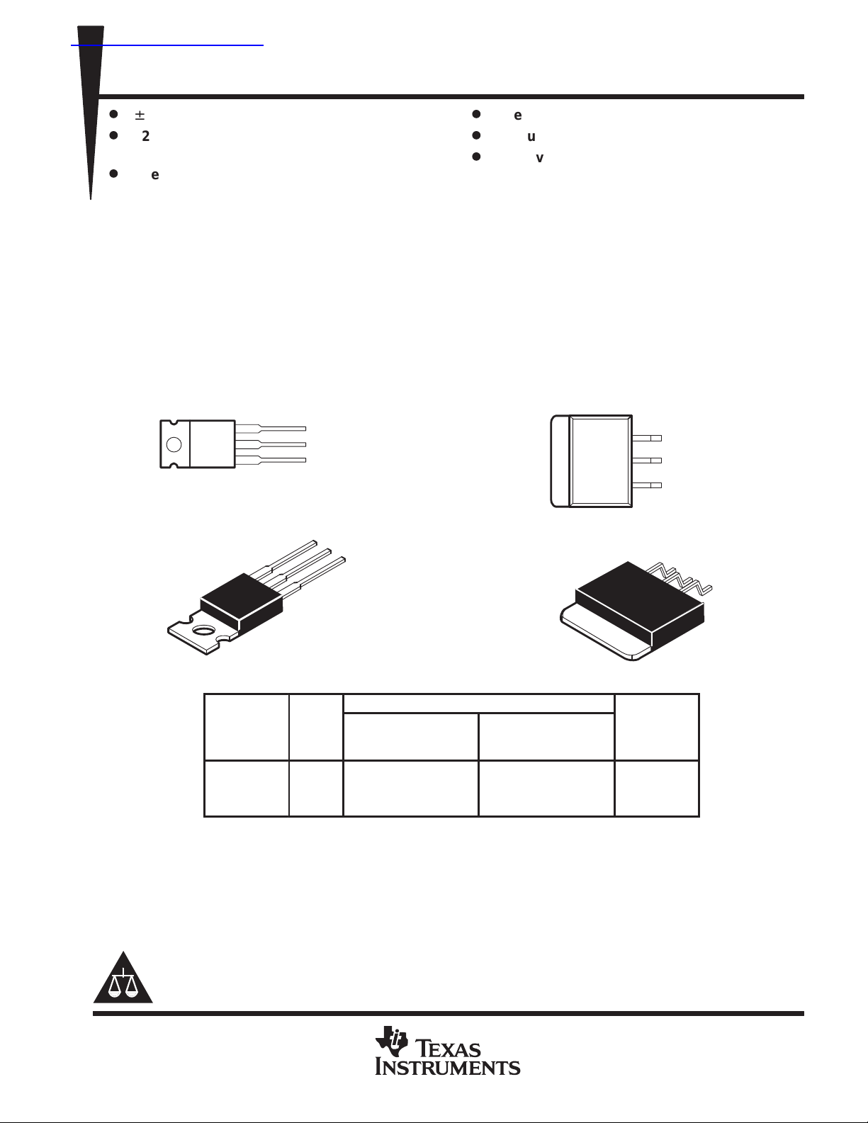
TL780 SERIES
KC PACKAGE
(TOP VIEW)
OUTPUT
COMMON
INPUT
The COMMON terminal is in electrical
contact with the mounting base.
TO-220AB
T
J
0°C to 125°C
The KTE package is available taped and reeled. Add the suffix R to the device type (e.g.,
TL780-05CKTER). Chip forms are tested at 25°C.
O
C
I
AVAILABLE OPTIONS
PACKAGED DEVICES
VO TYP
HEAT-SINK MOUNTED
(V)
5 TL780-05CKC TL780-05CKTE TL780-05Y
12 TL780-12CKC TL780-12CKTE TL780-12Y
15 TL780-15CKC TL780-15CKTE TL780-15Y
(KC)
FLANGE MOUNTED
The COMMON terminal is in electrical
contact with the mounting base.
PLASTIC
(KTE)
KTE PACKAGE
(TOP VIEW)
FORM
(Y)
OUTPUT
COMMON
INPUT
O
C
I
Please be aware that an important notice concerning availability, standard warranty, and use in critical applications of
Texas Instruments semiconductor products and disclaimers thereto appears at the end of this data sheet.
PRODUCTION DATA information is current as of publication date.
Products conform to specifications per the terms of Texas Instruments
standard warranty. Production processing does not necessarily include
testing of all parameters.
POST OFFICE BOX 655303 • DALLAS, TEXAS 75265
Copyright 1999, Texas Instruments Incorporated
1
Page 2
TL780 SERIES
POSITIVE-VOLTAGE REGULATORS
SLVS055F – APRIL 1981 – REVISED DECEMBER 1999
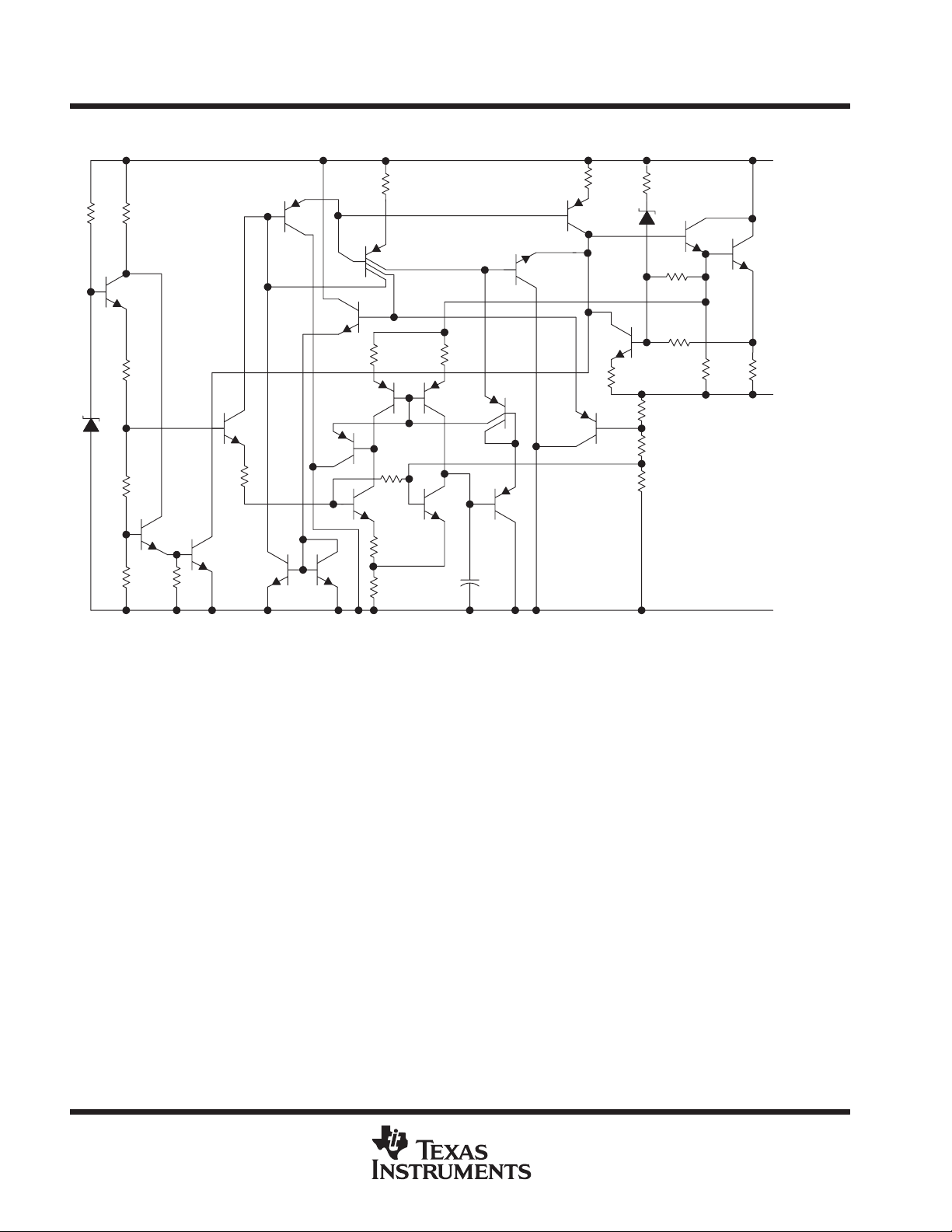
schematic
INPUT
OUTPUT
COMMON
2
POST OFFICE BOX 655303 • DALLAS, TEXAS 75265
Page 3
PARAMETER
TEST CONDITIONS
T
‡
UNIT
Output voltage
O
,
,
V
Input voltage regulation
25°C
mV
Output voltage regulation
25°C
mV
Input bias-current change
0°C to 125°C
mA
TL780 SERIES
POSITIVE-VOLTAGE REGULATORS
SLVS055F – APRIL 1981 – REVISED DECEMBER 1999
absolute maximum ratings over operating temperature range (unless otherwise noted)
†
Input voltage, VI 35 V. . . . . . . . . . . . . . . . . . . . . . . . . . . . . . . . . . . . . . . . . . . . . . . . . . . . . . . . . . . . . . . . . . . . . . . . . . .
Package thermal impedance, θJA (see Notes 1 and 2): KC package 22°C/W. . . . . . . . . . . . . . . . . . . . . . . . . . .
KTE package 23°C/W. . . . . . . . . . . . . . . . . . . . . . . . .
Operating free-air, T
; case, TC; or virtual junction, TJ, temperature range 0°C to 150°C. . . . . . . . . . . . . . . . .
A
Lead temperature 1,6 mm (1/16 inch) from case for 10 seconds 260°C. . . . . . . . . . . . . . . . . . . . . . . . . . . . . . .
Storage temperature range, T
†
Stresses beyond those listed under “absolute maximum ratings” may cause permanent damage to the device. These are stress ratings only, and
functional operation of the device at these or any other conditions beyond those indicated under “recommended operating conditions” is not
implied. Exposure to absolute-maximum-rated conditions for extended periods may affect device reliability.
NOTES: 1. Maximum power dissipation is a function of TJ(max),
ambient temperature is PD = (TJ(max) – TA)/
variations in individual device electrical characteristics and thermal resistance, the built-in thermal overload protection may be
activated at power levels slightly above or below the rated dissipation.
2. The package thermal impedance is calculated in accordance with JESD 51.
–65°C to 150°C. . . . . . . . . . . . . . . . . . . . . . . . . . . . . . . . . . . . . . . . . . . . . . . . . . .
stg
θ
, and TA. The maximum allowable power dissipation at any allowable
θ
JA
JA
. Operating at the absolute maximum TJ of 150°C can impact reliability. Due to
recommended operating conditions
MIN MAX UNIT
TL780-05C 7 25
Input voltage, V
Output current, I
Operating virtual junction temperature, T
I
O
J
TL780-12C 14.5 30 V
TL780-15C 17.5 30
1.5 A
0 125 °C
electrical characteristics at specified virtual junction temperature, VI = 10 V, IO = 500 mA (unless
otherwise noted)
J
I
p
p
Ripple rejection VI = 8 V to 18 V, f = 120 Hz 0°C to 125°C 70 85 dB
p
Output resistance f = 1 kHz 0°C to 125°C 0.0035 W
Temperature coefficient of output voltage IO = 5 mA 0°C to 125°C 0.25 mV/°C
Output noise voltage f = 10 Hz to 100 kHz 25°C 75 µV
Dropout voltage IO = 1 A 25°C 2 V
Input bias current 25°C 5 8 mA
p
Short-circuit output current 25°C 750 mA
Peak output current 25°C 2.2 A
‡
Pulse-testing techniques maintain the junction temperature as close to the ambient temperature as possible. Thermal effects must be taken into
account separately . All characteristics are measured with a 0.33-µF capacitor across the input and a 0.22-µF capacitor across the output.
= 5 mA to 1 A, P ≤ 15 W,
VI = 7 V to 20 V
VI = 7 V to 25 V
VI = 8 V to 12 V
IO = 5 mA to 1.5 A
IO = 250 mA to 750 mA
VI = 7 V to 25 V
IO = 5 mA to 1 A
25°C 4.95 5 5.05
0°C to 125°C 4.9 5.1
°
°
°
°
TL780-05C
MIN TYP MAX
0.5 5
0.5 5
4 25
1.5 15
0.7 1.3
0.003 0.5
POST OFFICE BOX 655303 • DALLAS, TEXAS 75265
3
Page 4

TL780 SERIES
PARAMETER
TEST CONDITIONS
T
†
UNIT
Output voltage
O
,
,
V
Input voltage regulation
25°C
mV
Output voltage regulation
25°C
mV
Input bias-current change
0°C to 125°C
mA
PARAMETER
TEST CONDITIONS
T
†
UNIT
Output voltage
V
Input voltage regulation
25°C
mV
Output voltage regulation
25°C
mV
Input bias-current change
0°C to 125°C
mA
POSITIVE-VOLTAGE REGULATORS
SLVS055F – APRIL 1981 – REVISED DECEMBER 1999
electrical characteristics at specified virtual junction temperature, VI = 19 V, IO = 500 mA (unless
otherwise noted)
J
I
p
p
Ripple rejection VI = 15 V to 25 V, f = 120 Hz 0°C to 125°C 65 80 dB
p
Output resistance f = 1 kHz 0°C to 125°C 0.0035 W
Temperature coefficient of output voltage IO = 5 mA 0°C to 125°C 0.6 mV/°C
Output noise voltage f = 10 Hz to 100 kHz 25°C 180 µV
Dropout voltage IO = 1 A 25°C 2 V
Input bias current 25°C 5.5 8 mA
p
Short-circuit output current 25°C 350 mA
Peak output current 25°C 2.2 A
†
Pulse-testing techniques maintain the junction temperature as close to the ambient temperature as possible. Thermal effects must be taken into
account separately . All characteristics are measured with a 0.33-µF capacitor across the input and a 0.22-µF capacitor across the output.
= 5 mA to 1 A, P ≤ 15 W,
VI = 14.5 V to 27 V
VI = 14.5 V to 30 V
VI = 16 V to 22 V
IO = 5 mA to 1.5 A
IO = 250 mA to 750 mA
VI = 14.5 V to 30 V
IO = 5 mA to 1 A
25°C 11.88 12 12.12
0°C to 125°C 11.76 12.24
°
°
°
°
TL780-12C
MIN TYP MAX
1.2 12
1.2 12
6.5 60
2.5 36
0.4 1.3
0.03 0.5
electrical characteristics at specified virtual junction temperature, VI = 23 V, IO = 500 mA (unless
otherwise noted)
J
p
p
Ripple rejection VI = 18.5 V to 28.5 V, f = 120 Hz 0°C to 125°C 60 75 dB
p
Output resistance f = 1 kHz 0°C to 125°C 0.0035 W
Temperature coefficient of output voltage IO = 5 mA 0°C to 125°C 0.62 mV/°C
Output noise voltage f = 10 Hz to 100 kHz 25°C 225 µV
Dropout voltage IO = 1 A 25°C 2 V
Input bias current 25°C 5.5 8 mA
p
Short-circuit output current 25°C 230 mA
Peak output current 25°C 2.2 A
†
Pulse-testing techniques maintain the junction temperature as close to the ambient temperature as possible. Thermal effects must be taken into
account separately . All characteristics are measured with a 0.33-µF capacitor across the input and a 0.22-µF capacitor across the output.
IO = 5 mA to 1 A,
VI = 17.5 V to 30 V
VI = 17.5 V to 30 V
VI = 20 V to 26 V
IO = 5 mA to 1.5 A
IO = 250 mA to 750 mA
VI = 17.5 V to 30 V
IO = 5 mA to 1 A
P ≤ 15 W,
25°C
0°C to 125°C
°
°
°
°
TL780-15C
MIN TYP MAX
14.85 15 15.15
14.7 15.3
1.5 15
1.5 15
7 75
2.5 45
0.4 1.3
0.02 0.5
4
POST OFFICE BOX 655303 • DALLAS, TEXAS 75265
Page 5

PARAMETER
TEST CONDITIONS
†
UNIT
Input voltage regulation
mV
Output voltage regulation
mV
PARAMETER
TEST CONDITIONS
†
UNIT
Input voltage regulation
mV
Output voltage regulation
mV
TL780 SERIES
POSITIVE-VOLTAGE REGULATORS
SLVS055F – APRIL 1981 – REVISED DECEMBER 1999
electrical characteristics, VI = 10 V, IO = 500 mA, TJ = 25°C (unless otherwise noted)
TL780-05Y
MIN TYP MAX
Output voltage IO = 5 mA to 1 A, P ≤ 15 W 5 V
p
p
Output noise voltage f = 10 Hz to 100 kHz 75 µV
Dropout voltage IO = 1 A 2 V
Input bias current 5 mA
Short-circuit output current 750 mA
Peak output current 2.2 A
†
Pulse-testing techniques maintain the junction temperature as close to the ambient temperature as possible. Thermal effects must be taken into
account separately . All characteristics are measured with a 0.33-µF capacitor across the input and a 0.22-µF capacitor across the output.
electrical characteristics, VI = 19 V, IO = 500 mA, TJ = 25°C (unless otherwise noted)
Output voltage IO = 5 mA to 1 A, P ≤ 15 W 12 V
p
p
Output noise voltage f = 10 Hz to 100 kHz 180 µV
Dropout voltage IO = 1 A 2 V
Input bias current 5.5 mA
Short-circuit output current 350 mA
Peak output current 2.2 A
†
Pulse-testing techniques maintain the junction temperature as close to the ambient temperature as possible. Thermal effects must be taken into
account separately . All characteristics are measured with a 0.33-µF capacitor across the input and a 0.22-µF capacitor across the output.
VI = 7 V to 25 V 0.5
VI = 8 V to 12 V 0.5
IO = 5 mA to 1.5 A 4
IO = 250 mA to 750 mA 1.5
TL780-12Y
MIN TYP MAX
VI = 14.5 V to 30 V 1.2
VI = 16 V to 22 V 1.2
IO = 5 mA to 1.5 A 6.5
IO = 250 mA to 750 mA 2.5
POST OFFICE BOX 655303 • DALLAS, TEXAS 75265
5
Page 6

TL780 SERIES
PARAMETER
TEST CONDITIONS
†
UNIT
Input voltage regulation
mV
Output voltage regulation
mV
POSITIVE-VOLTAGE REGULATORS
SLVS055F – APRIL 1981 – REVISED DECEMBER 1999
electrical characteristics, VI = 23 V, IO = 500 mA, TJ = 25°C (unless otherwise noted)
TL780-15Y
MIN TYP MAX
Output voltage IO = 5 mA to 1 A, P ≤ 15 W 15 V
p
p
Output resistance f = 1 kHz 0.0035 W
Output noise voltage f = 10 Hz to 100 kHz 225 µV
Dropout voltage IO = 1 A 2 V
Input bias current 5.5 mA
Short-circuit output current 230 mA
Peak output current 2.2 A
†
Pulse-testing techniques maintain the junction temperature as close to the ambient temperature as possible. Thermal effects must be taken into
account separately . All characteristics are measured with a 0.33-µF capacitor across the input and a 0.22-µF capacitor across the output.
VI = 17.5 V to 30 V 1.5
VI = 20 V to 26 V 1.5
IO = 5 mA to 1.5 A 7
IO = 250 mA to 750 mA 2.5
PARAMETER MEASUREMENT INFORMATION
INPUT
C1 = 0.33 µF
(see Note A)
NOTES: A. C1 is required when the regulator is far from the power-supply filter .
B. C2 is not required for stability; however, transient response is improved.
C. Permanent damage can occur when OUTPUT is pulled below ground.
Figure 1. Test Circuit
TL780
C
OI
OUTPUT
(see Note C)
C2 = 0.22 µF
(see Note B)
6
POST OFFICE BOX 655303 • DALLAS, TEXAS 75265
Page 7

TL780 SERIES
POSITIVE-VOLTAGE REGULATORS
SLVS055F – APRIL 1981 – REVISED DECEMBER 1999
APPLICATION INFORMATION
TL780-xx
VO(Reg)
R1
I
O
+
–
V
I
In
TL780-xx
COMMON
Out
GND
I
L
–V
INPUT
C1
0.33 µF
O
IO = (VO/R1) + IO Bias Current
Figure 2. Positive Regulator in Negative
Configuration (VI Must Float)
Figure 3. Current Regulator
operation with a load common to a voltage of opposite polarity
In many cases, a regulator powers a load that is not connected to ground but, instead, is connected to a voltage
source of opposite polarity (e.g., operational amplifiers, level-shifting circuits, etc.). In these cases, a clamp
diode should be connected to the regulator output as shown in Figure 4. This protects the regulator from output
polarity reversals during startup and short-circuit operation.
V
I
Figure 4. Output Polarity-Reversal-Protection Circuit
TL780-xx
1N4001
or
Equivalent
–V
V
O
O
OUTPUT
reverse-bias protection
Occasionally , the input voltage to the regulator can collapse faster than the output voltage. This, for example,
could occur when the input supply is crowbarred during an output overvoltage condition. If the output voltage
is greater than approximately 7 V, the emitter-base junction of the series pass element (internal or external)
could break down and be damaged. To prevent this, a diode shunt can be employed, as shown in Figure 5.
V
I
TL780-xx
Figure 5. Reverse-Bias-Protection Circuit
V
O
POST OFFICE BOX 655303 • DALLAS, TEXAS 75265
7
Page 8

IMPORTANT NOTICE
T exas Instruments and its subsidiaries (TI) reserve the right to make changes to their products or to discontinue
any product or service without notice, and advise customers to obtain the latest version of relevant information
to verify, before placing orders, that information being relied on is current and complete. All products are sold
subject to the terms and conditions of sale supplied at the time of order acknowledgement, including those
pertaining to warranty, patent infringement, and limitation of liability.
TI warrants performance of its semiconductor products to the specifications applicable at the time of sale in
accordance with TI’s standard warranty. Testing and other quality control techniques are utilized to the extent
TI deems necessary to support this warranty . Specific testing of all parameters of each device is not necessarily
performed, except those mandated by government requirements.
CERTAIN APPLICA TIONS USING SEMICONDUCT OR PRODUCTS MAY INVOLVE POTENTIAL RISKS OF
DEATH, PERSONAL INJURY, OR SEVERE PROPERTY OR ENVIRONMENTAL DAMAGE (“CRITICAL
APPLICATIONS”). TI SEMICONDUCTOR PRODUCTS ARE NOT DESIGNED, AUTHORIZED, OR
WARRANTED TO BE SUITABLE FOR USE IN LIFE-SUPPORT DEVICES OR SYSTEMS OR OTHER
CRITICAL APPLICA TIONS. INCLUSION OF TI PRODUCTS IN SUCH APPLICATIONS IS UNDERST OOD TO
BE FULLY AT THE CUSTOMER’S RISK.
In order to minimize risks associated with the customer’s applications, adequate design and operating
safeguards must be provided by the customer to minimize inherent or procedural hazards.
TI assumes no liability for applications assistance or customer product design. TI does not warrant or represent
that any license, either express or implied, is granted under any patent right, copyright, mask work right, or other
intellectual property right of TI covering or relating to any combination, machine, or process in which such
semiconductor products or services might be or are used. TI’s publication of information regarding any third
party’s products or services does not constitute TI’s approval, warranty or endorsement thereof.
Copyright 1999, Texas Instruments Incorporated
 Loading...