

Page 1

TL7231MD
FULL LAYER-III ISO/IEC 11172-3 AUDIO DECODER
n Single-chip ISO/IEC 11172-3 Layer
III Audio Decoder
n Supports All MPEG Bit Rates
Including Free Format
n Supports 32/44.1/48KHz Sampling
Frequencies for MPEG Bit Stream
n Supports Single Channel, Dual
Channel, Stereo, and Joint Stereo
n Any Combination of Intensity
Stereo and MS Stereo is
supported.
n Serial Bit Stream Input
n 8-bit Host Interface Port
n Digital Volume Control
n Digital Bass/Treble Control
n 6-Band Equalizer Function
n Voice Record/Playback Capability
n On-chip DAC with 1-bit Sigma Delta
Modulation
n Supports Off-chip DAC Interface
n On-chip ADC with 12-bit Resolution
n Power Management to Reduce
Power Consumption
n PLL for Internal Clocks and for
Output PCM Clock Generation
n Single 16.9344MHz External Clock
Input
n 3.0 V Operation
n Small Footprint 100-pin Thin Quad
Flat Package
DESCRIPTION
TL7231MD is a single-chip ISO/IEC 11172-3 Layer III audio decoder, capable of decoding
compressed elementary bit streams as specified in ISO/IEC standard. Since it integrated onchip ADC and on-chip DAC, it can provide you more small and cheaper solution for MP3 player
application. It is designed to be well suited for portable audio appliances.
TL7231MD receives the input data bit stream through a serial data interface. The decoded
signal is 16-bit serial PCM format that can be sent directly to DAC. The generated PCM data
can be sent to on-chip DAC or off-chip DAC according to user preference. The off-chip DAC
interface is programmable to adapt the PCM output of TL7231MD to the most common DACs
used on the market.
An 8-bit host interface port is provided to receive control information from and send status
information to host. 8-bit microcontrollers such as those of Intel or Motorola can be connected
easily.
TL7231MD has the capability of compressing voice signals. It can receive voice signals through
on-chip ADC. The compressed voice signals are transmitted to or received from host through
serial data interface. It can also reproduce the voice signals from the compressed voice signals.
September 1999 1/37
Page 2
TL7231MD
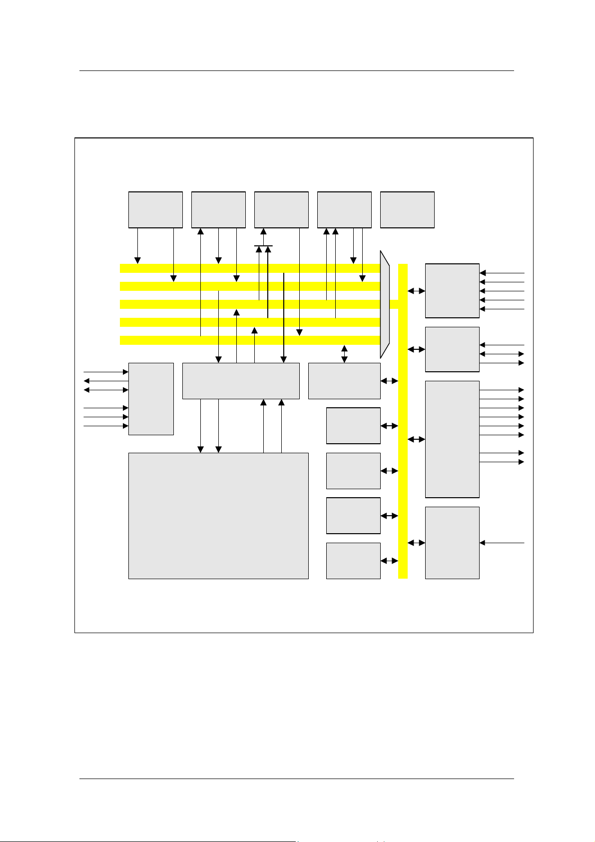
FUNCTIONAL BLOCK DIAGRAM
CPUXI
CPUXO
FILTER
RESET
WAKEUP
PWRDN
CONSTANT
ROM
DATA READ0
DATA READ1
DATA WRITE0
DATA WRITE1
DMA BUS
RESET/
CLOCK
UNIT
INPUT
BUFFER
OUTPUT
BUFFER
BUS CONTROL UNIT
READ DATA1
READ DATA0
WRITE DATA0
WRITE DATA1
WORKING
SPACE
DMA
CONTROLLER
CRC
SERIAL0
PROGRAM
ROM
M
U
X
HOST
INTERFACE
SERIAL1
DAC
HD7:0
HALE
HRD#
HWR#
HSEL#
CLKXRM
DXRM
REQSTRM
DACMSCK
DACBCK
DACLRCK
DACSDATA
DACDEEM
DACMUTE#
AOUTL
AOUTR
DSP Core Unit
TIMER0
ADC
ADCAIN
TIMER1
Figure 1. Functional Block Diagram of TL7231MD
2/37 SAMSUNG Electronics Co.
Page 3

PIN DESCRIPTION
DACVREF
AOUTL
DACVBB
VSS
97
98
99
DACVSSA
DACVDDA
DACVHALF
AOUTR
DACVSSD
DACVDDD
ADCAIN
ADCVSSA
ADCVBB
ADCVDDA
ADCREFN
ADCREFP
ADCVSSD
ADCVDDD
PLLVDDA
PLLVSSA
PLLVBB
FILTER
CPUXO
CPUXI
VDD
VSS
BCLK
VDD
VSS
100
1
2
3
4
5
6
7
8
9
10
11
12
13
14
15
16
17
18
19
20
21
22
23
24
25
26272829303132333435363738394041424344454647484950
NC
VSSNCVSS
95
96
NC
NC
NC
VSS
VDDIO
VDD
89
90
91
92
93
94
VSSIO
86
87
88
TL7231MD
TOP VIEW
DACMUTE#
DACDEEM
84
85
DACSDATA
DACLRCK
DACBCK
81
82
83
DACMSCK
VSS
79
80
VSS
78
VSS
77
VSS
76
75
74
73
72
71
70
69
68
67
66
65
64
63
62
61
60
59
58
57
56
55
54
53
52
51
TL7231MD
VSS
VSS
VSS
VSS
VDD
NC
NC
NC
VDD
VSS
VDDIO
VSSIO
CLKXRM
DXRM
REQSTRM
VDD
HALE
HSEL#
HRD#
HWR#
HD7
HD6
HD5
HD4
HD3
VDDIO
VSSIO
RESET
PWRDN
WAKEUP
VSS
VSS
VSS
VSS
VSS
VSS
VDD
VSS
VDDIO
NCNCNC
VSSIO
NC
VSS
VSS
VSS
HD0
HD1
HD2
Figure 2. 100-pin Thin Quad Flat Package (TQFP)
SAMSUNG Electronics CO. 3/37
Page 4

TL7231MD
PIN
1 DACVSSA 26 VDDIO 51 HD3 76 VSS
2 DACVDDA 27 VSSIO 52 HD4 77 VSS
3 DACVHALF 28 RESET 53 HD5 78 VSS
4 AOUTR 29 WAKEUP 54 HD6 79 VSS
5 DACVSSD 30 PWRDN 55 HD7 80 DACMSCK
6 DACVDDD 31 VSS 56 HWR# 81 DACBCK
7 ADCAIN 32 VSS 57 HRD# 82 DACLRCK
8 ADCVSSA 33 VSS 58 HSEL# 83 DACSDATA
9 ADCVBB 34 VSS 59 HALE 84 DACDEEM
10 ADCVDDA 35 VSS 60 VDD 85 DACMUTE#
11 ADCREFN 36 VSS 61 REQSTRM 86 VSSIO
12 ADCREFP 37 VDD 62 DXRM 87 VDDIO
13 ADCVSSD 38 VSS 63 CLKXRM 88 VSS
14 ADCVDDD 39 VDDIO 64 VSSIO 89 VDD
15 PLLVDDA 40 VSSIO 65 VDDIO 90 NC
16 PLLVSSA 41 NC 66 VSS 91 NC
17 PLLVBB 42 NC 67 VDD 92 NC
18 FILTER 43 NC 68 NC 93 VSS
19 CPUXO 44 NC 69 NC 94 NC
20 CPUXI 45 VSS 70 NC 95 VSS
21 VDD 46 VSS 71 VDD 96 NC
22 VSS 47 VSS 72 VSS 97 VSS
23 BCLK 48 HD0 73 VSS 98 DACVBB
24 VDD 49 HD1 74 VSS 99 AOUTL
25 VSS 50 HD2 75 VSS 100 DACVREF
NAME PIN
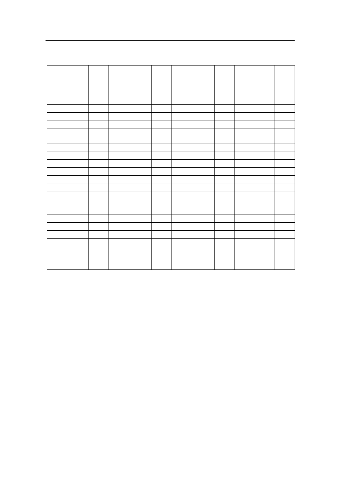
Table 1. Pin Locations with Pin Names
NAME PIN NAME PIN
NAME
4/37 SAMSUNG Electronics Co.
Page 5
NAME PIN NAME PIN NAME PIN
ADCAIN 7 DACVSSA 1 NC 92 VSS 34
ADCREFN 11 DACVSSD 5 NC 94 VSS 35
ADCREFP 12 DXRM 62 NC 96 VSS 36
ADCVBB 9 FILTER 18 PLLVBB 17 VSS 38
ADCVDDA 10 HD0 48 PLLVDDA 15 VSS 45
ADCVDDD 14 HD1 49 PLLVSSA 16 VSS 46
ADCVSSA 8 HD2 50 PWRDN 30 VSS 47
ADCVSSD 13 HD3 51 REQSTRM 61 VSS 66
AOUTL 99 HD4 52 RESET 28 VSS 72
AOUTR 4 HD5 53 VDD 21 VSS 73
BCLK 23 HD6 54 VDD 24 VSS 74
CLKXRM 63 HD7 55 VDD 37 VSS 75
CPUXI 20 HALE 59 VDD 60 VSS 76
CPUXO 19 HRD# 57 VDD 67 VSS 77
DACBCK 81 HSEL# 58 VDD 71 VSS 78
DACDEEM 84 HWR# 56 VDD 89 VSS 79
DACLRCK 82 NC 41 VDDIO 26 VSS 88
DACMSCK 80 NC 42 VDDIO 39 VSS 93
DACMUTE# 85 NC 43 VDDIO 65 VSS 95
DACSDATA 83 NC 44 VDDIO 87 VSS 97
DACVBB 98 NC 68 VSS 22 VSSIO 27
DACVDDA 2 NC 69 VSS 25 VSSIO 40
DACVDDD 6 NC 70 VSS 31 VSSIO 64
DACVHALF 3 NC 90 VSS 32 VSSIO 86
DACVREF 100 NC 91 VSS 33 WAKEUP 29
Table 2. Pin Functions with Location
TL7231MD
NAME PIN
SAMSUNG Electronics CO. 5/37
Page 6

TL7231MD
Signal Name Type Description
CPUXI I CPU Clock In. 16.9344MHz crystal clock input.
CPUXO O CPU Clock Out. 16.9344MHz crystal clock output.
FILTER O
BCLK O Processor Clock Output.
RESET I Chip Reset. Reset input to the chip. Internal pull down.
WAKEUP I
PWRDN I
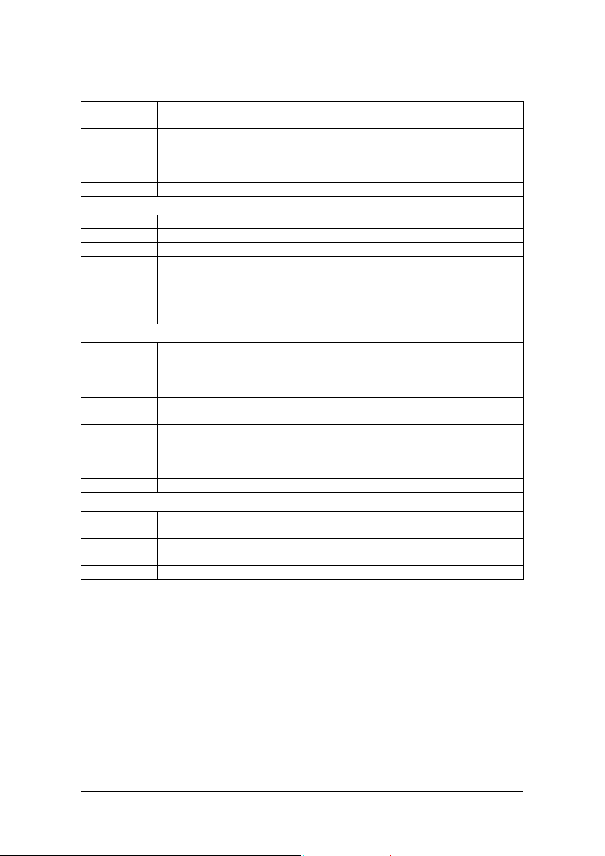
Table 3. Pin Descriptions
Internal PLL Interface
Charge Pump Out. External capacitor should be connected
between this pin and analog ground.
Clock Signal
Reset & Power Down Control
Wake Up. When high, chip is waked up from SLEEP state. This pin
should be remained active at least 1 clock cycle and inactive before
the host issues next SLEEP command. Internal pull down.
Power Down. This pin controls PWRDOWN state. When high, chip
goes to very low power consumption state. After deactivation,
WAKEUP pin should be remained low at least 150µs. Internal pull
down.
(Restriction: This pin should be active ONLY in SLEEP state.
Otherwise, Chip reset should be activated.)
MCU Serial Interface
CLKXRM I Serial Clock. MCU serial interface clock.
Serial Data. When MCU transmits data, this data pin is sampled at
negative edge of CLKXRM. When MCU receives data, Data is valid
DXRM I/O
REQSTRM O
HSEL# I HIP Enable. When Low, HIP is selected.
HALE I
HRD# I
HWR# I
HD[7:0] I/O HIP Address/Data Bus. Multiplexed address lines and data lines.
ADCAIN I
ADCREFP I
ADCREFN I ADC Internal Reference Bottom Bias. Connect this pin to ground.
from negative edge of CLKXRM to next negative edge of CLKXRM.
DXRM should be sampled at positive edge of CLKXRM. After reset,
TL7231MD is set to transmit the most significant bit first.
Request Bit Stream Data. MCU must check this pin to determine to
continue receiving or transmitting. MCU should transmit or receive
data during this signal active.
MCU HIP(Host Interface Port) Interface
HIP Address Latch Enable. When High, HD[7:0] should have HIP
address, which is sampled at negative edge of this signal.
HIP Read Enable. When low, data is loaded to HD[7:0], which
should be sampled at positive edge of this signal.
HIP Write Enable. Data at HD[7:0] is sampled at positive edge of
this signal.
Internal ADC Interface
ADC Analog Input. Analog input spans between ADCREFP and
ADCREFN.
ADC Internal Reference Top Bias. Connect this pin to voltage
between ADCVDDA and 2.0V.
6/37 SAMSUNG Electronics Co.
Page 7
TL7231MD
ADCVDDA PWR
ADC Supply Voltage for Analog Circuit. Connect this pin to the
+3.0V supply voltage.
ADCVSSA GND ADC Ground for Analog Circuit. Connect this pin to ground.
ADCVDDD PWR
ADC Supply Voltage for Digital Circuit. Connect this pin to the
+3.0V supply voltage.
ADCVSSD GND ADC Ground for Digital Circuit. Connect this pin to ground.
ADCVBB GND ADC Analog/Digital Bulk Bias. Connect this pin to ground.
External DAC Interface
DACMSCK O DAC Master Clock. 384×Fs clock.
DACBCK O DAC Bit Clock. 32×Fs clock.
DACLRCK O DAC Sample Rate Clock. Fs clock.
DACSDATA O DAC Serial Data. Serial data.
DACDEEM O
DACMUTE# O
DAC Deemphasis. When deemphasis is on, this signal is high. It
can be set/clear through HIP commands.
DAC Mute. Analog output mute. When external DAC is set to mute
on, this signal is low. It can be set/clear through HIP commands.
Internal DAC Interface
AOUTL O Analog Output for Left-Channel.
AOUTR O Analog Output for Right-Channel.
DACVHALF I/O DAC Reference Voltage Output for Bypass.
DACVREF I/O DAC Reference Voltage Output for Bypass.
DACVDDA PWR
DAC Supply Voltage for Analog Circuit. Connect this pin to the
+3.0V supply voltage.
DACVSSA GND DAC Ground for Analog Circuit. Connect this pin to ground.
DACVDDD PWR
DAC Supply Voltage for Digital Circuit. Connect this pin to the
+3.0V supply voltage.
DACVSSD GND DAC Ground for Digital Circuit. Connect this pin to ground.
DACVBB GND DAC Pad Bulk Bias. Connect this pin to ground.
Power/Ground Pins
VDD PWR Supply Voltage. Connect this pin to the +3.0V supply voltage.
VSS GND Circuit Ground. Connect this pin to ground.
VDDIO PWR
Supply Voltage for I/O Buffers. Connect this pin to the +3.0V
supply voltage.
VSSIO GND Circuit Ground for I/O Buffers. Connect this pin to ground.
SAMSUNG Electronics CO. 7/37
Page 8
TL7231MD
FUNCTIONAL DESCRIPTION
RESET/CLOCK UNIT
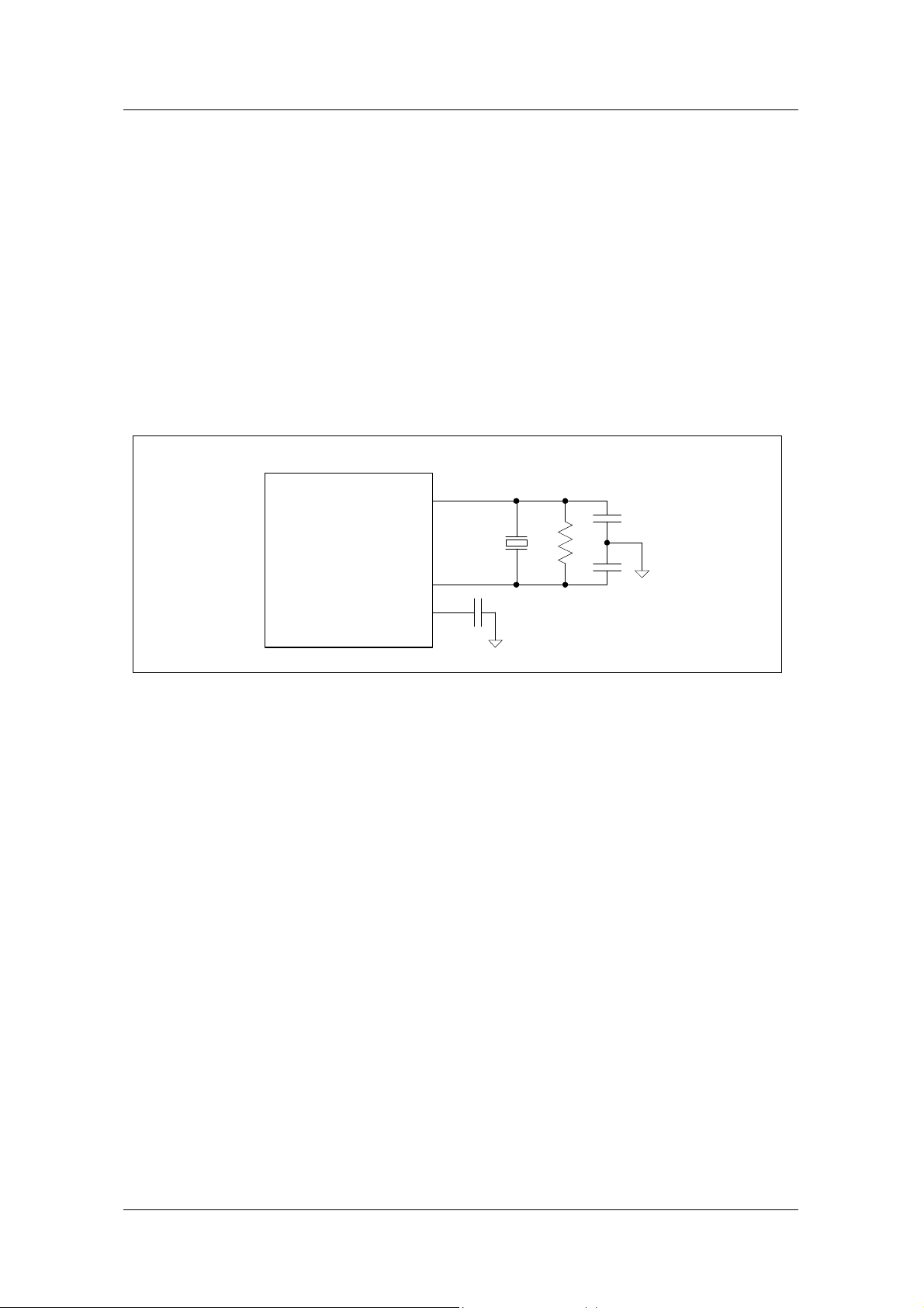
TL7231MD is driven by a single clock at the frequency of 16.9344MHz. The clock is derived
from an external source or from an industry standard crystal oscillator, generating input
frequency of 16.9344MHz. The clock generation unit has a PLL, and all the internal clock
signals including internal DAC/ADC clocks are generated with the input clock.
When TL7231MD is in power-on-reset, RESET signal should be active at least 150µs till the
internal PLL is stabilized. To reset TL7231MD during normal operation, RESET signal should be
active at least 16 cycles.
TL7231MD
CPUXI
30p
16.9344MHz
CPUXO
1M
30p
FILTER
820p
Figure 3. Clock Circuit
DSP CORE LOGIC
The core logic of TL7231MD is a 32-bit floating-point DSP processor. The independent multiplier
and accumulator of TL7231MD can achieve high performance. Internal registers are 40-bit
registers that store values with a 32-bit mantissa and an 8-bit exponent. These registers can
serve as both the source and destination for any arithmetic operation. Since all the data
input/output transactions are managed by DMA, there is no computational overhead due to data
transactions.
SERIAL INTERFACE
The serial interface of TL7231MD is used to receive MPEG bit stream data or transmit/receive
voice data. It is configured to transfer 8 bits of data per word. It can be configured to be LSBfirst or MSB first transfer mode. LSB-first means that the data bits are transmitted and received
least-significant bit (LSB) first. MSB-first means that the data bits are transmitted and received
most-significant bit (MSB) first. The clock for the serial interface should be generated externally.
The related signals are CLKXRM, DXRM, and REQSTRM. REQSTRM is used for
synchronization between microcontroller and TL7231MD, and data is transferred during
REQSTRM active.
8/37 SAMSUNG Electronics Co.
Page 9

When microcontroller tries to send data to TL7231MD, it should check whether REQSTRM is
active or not. If the signal is active, microcontroller sets its serial interface to transmit mode and
send serial clock and serial data. After transmitting each byte, microcontroller should check
REQSTRM to decide whether next byte is to be transmitted or not.
When microcontroller tries to receive data from TL7231MD, it should check whether REQSTRM
is active or not. If the signal is active, microcontroller sets its serial interface to receive mode
and send serial clock and receive serial data from TL7231MD. After receiving each byte,
microcontroller should check REQSTRM to decide whether TL7231MD will transmit next byte or
not.
TL7231MD
HOST INTERFACE PORT (HIP)
Host interface port is used to send commands to and receive status information from
TL7231MD. HIP of TL7231MD is a parallel I/O port that makes a connection to a host processor
easily. Through the HIP, TL7231MD can be used as a memory-mapped peripheral to a host
processor. The HIP can be thought of as an area of dual-port memory that allows
communication between the computational core of the TL7231MD and host. The HIP is
completely asynchronous. The host processor can write data into the HIP while the TL7231MD
is operating at full speed. HIP transfers are managed using interrupt scheme.
HIP contains 21 registers. Four of them are data-in registers (HDI0/HDI1/HDI2/HDI3) and one of
them is a status register (HSR4). The remaining 16 registers are data-out registers
(HDO0/…/HDO15). Data written into HDIs by host are read by TL7231MD. Through these
registers host can give necessary commands to TL7231MD. A command is written into a HDI0,
and the required parameters of the command are written into the HDI1/HDI2/HDI3. The status
register (HSR4) keeps the information whether data written into the data-in registers are read by
TL7231MD. The status register is managed automatically by TL7231MD and can be read by
host. TL7231MD starts HIP command processing when HDI0 register is written. So if any
command requires parameters, user should write parameters first, and then write command.
Serial ID number can be used to check whether given command has been accepted or not.
TL7231MD can receive the serial ID value through HDO0 when TL7231MD has accepted the
given command. Thus when commands are given to TL7231MD with different serial ID numbers,
it can be examined which command is being processed. Serial ID number itself hasn’t any
special meaning. If this feature is not needed, it is not required to send ID values with
commands. Then the value of HDO0 is undetermined. There is an exception for the ID number
convention. If you use HIP command 0Dh(Revision Code), TL7231MD returns the TL7231MD
revision number, not the ID number.
HDOs are written by TL7231MD and can be read by host. All HIP registers should be memorymapped into the memory space of the host processor. The address space of those registers is
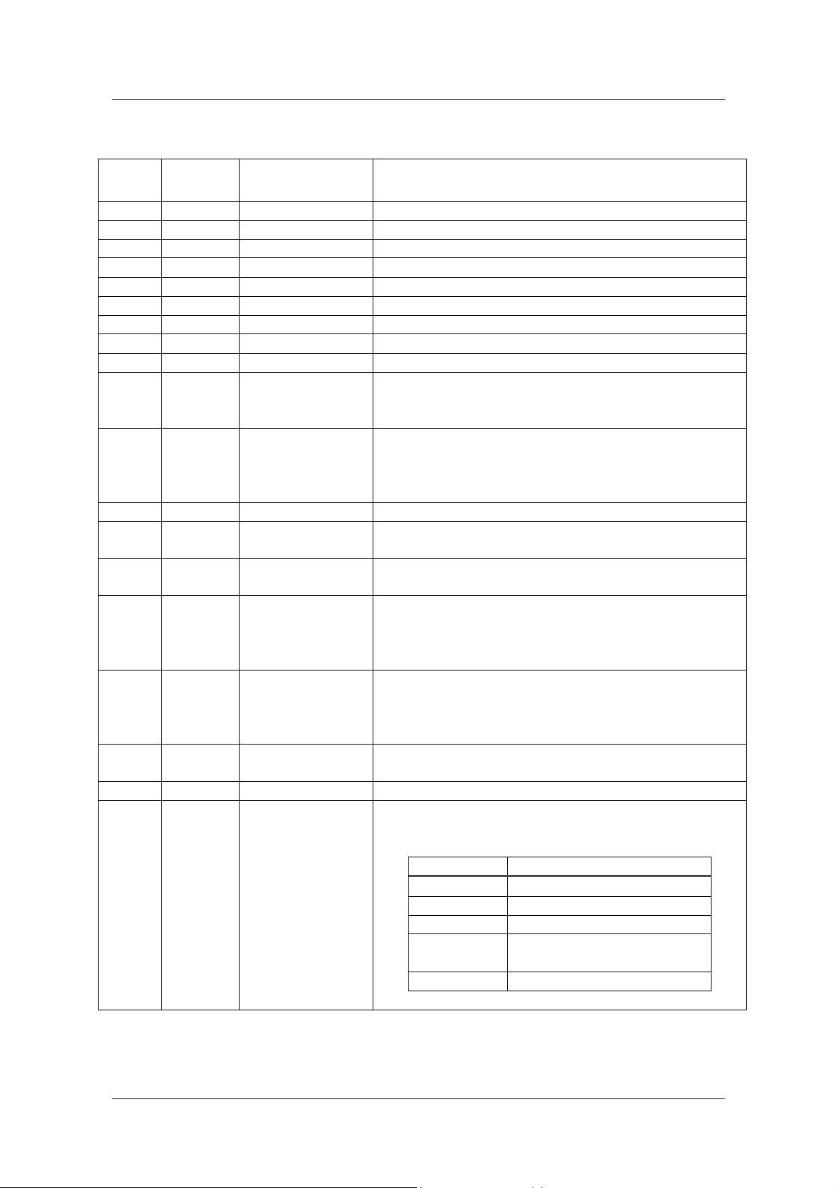
shown in Table 4. The usable commands are listed in Table 6. The contents reported by HDOs
are shown from Figure 4 to Figure 16.
Table 4. Address of Host Interface Port Registers
SAMSUNG Electronics CO. 9/37
Page 10

TL7231MD
ADDRESS REGISTERS DESCRIPTION
0h HDI0 Command
1h HDI1 Serial ID Number
2h ~ 3h HDI2/HDI3 Parameters if needed
4h HSR4 Status Register (Fig. 4)
10h HDO0 Command Serial ID Number (Fig. 5)
11h HDO1 Decoder State (Fig. 6)
12h HDO2 IO Status (Fig.7)
13h HDO3 IO Status (Fig. 8)
14h HDO4 Volume (Fig. 9)
15h HDO5 Serial Interface Mode (Fig. 10)
16h ~ 1Fh HDO6 ~ HDO15 The information provided by these registers depends on
The information provided by HDO6 to HDO15 depends on the mode setting of TL7231MD.
Refer to Table 5. The mode can be set by using HIP command 19h(Report Format). For this
command, refer to Table 6.
Table 5. The contents of HDO6 ~ HDO15 according to mode setting
ADDRESS REGISTERS DESCRIPTION
16h HDO6 Mode0: 00h
17h HDO7 Mode0: 00h
18h HDO8 Mode0: 00h
19h HDO9 Mode0: 00h
1Ah HDO10 Mode0: 00h
the mode setting of TL7231MD. (Refer to Table 5)
Mode1: Tone Control Status. When tone control is
enabled, 1 is reported. Otherwise, 0 is reported.
Mode2: MP3 Frame Count (Fig. 11)
Mode3: Voice Data Code Count (Fig. 11)
Mode4: Equalizer Control Status. When equalizer control
is enabled, 1 is reported. Otherwise, 0 is
reported.
Mode1: Tone Control - Prescaling Information
Mode2: MP3 Frame Count (Fig. 11)
Mode3: Voice Data Code Count (Fig. 11)
Mode4: EQ Control – Prescaling Information
Mode1: Tone Control – Bass Cutoff Frequency
Mode2: MP3 Frame Count (Fig. 11)
Mode3: Voice Data Code Count (Fig. 11)
Mode4: EQ Control – Band1 Gain
Mode1: Tone Control – Bass Gain
Mode2: MP3 Frame Count (Fig. 11)
Mode3: Voice Data Code Count (Fig. 11)
Mode4: EQ Control –Band2 Gain
10/37 SAMSUNG Electronics Co.
Page 11

Mode1: Tone Control – Treble Cutoff Frequency
Mode2: The most recently synchronized frame header of
MP3 bit stream. (Fig. 12)
Mode3: 00h
Mode4: EQ Control – Band3 Gain
1Bh HDO11 Mode0: 00h
Mode1: Tone Control – Treble Gain
Mode2: The most recently synchronized frame header of
MP3 bit stream. (Fig. 13)
Mode3: 00h
Mode4: EQ Control – Band4 Gain
1Ch HDO12 Mode0: 00h
Mode1: 00h
Mode2: The most recently synchronized frame header of
MP3 bit stream. (Fig. 14)
Mode3: 00h
Mode4: EQ Control – Band5 Gain
1Dh HDO13 Mode0: 00h
Mode1: 00h
Mode2: Bass Boost Information (Fig. 15)
Mode3: 00h
Mode4: EQ Control – Band6 Gain
1Eh HDO14 Mode0: 00h
Mode1: 00h
Mode2: DAC Output Valid (Fig. 16)
Mode3: 00h
Mode4: 00h
1Fh HDO15 Mode0: 00h
Mode1: 00h
Mode2: CRC Error Count
Mode3: 00h
Mode4: 00h
TL7231MD
SAMSUNG Electronics CO. 11/37
Page 12
TL7231MD
COMM
AND
00h None Stop Stop execution and go into WAIT state.
01h None MP3 Decoding Execute MP3 decoding.
04h None Voice Encoding Execute voice encoding (16Kbps).
05h None Voice Decoding Execute voice decoding (16Kbps).
06h None Voice Encoding Execute voice encoding (24Kbps).
07h None Voice Decoding Execute voice decoding (24Kbps).
08h None Voice Encoding Execute voice encoding (32Kbps).
09h None Voice Decoding Execute voice decoding (32Kbps).
0Dh None Revision Code Report the TL7231MD revision number in HDO0.
0Fh None Sleep Go into SLEEP state. This command should be used in
10h None Mute ON When using internal DAC, The output voltage level of
11h None Mute OFF Mute is disabled.
12h None Internal ADC Use Internal ADC. External ADC interfaces are disabled.
14h None Internal DAC Use internal DAC. After reset, it is set to use internal
15h None External DAC Use external DAC. Internal DAC is disabled. The
16h 1byte External DAC
17h None MSB First Serial Interface MSB-first mode. This is the default mode
18h None LSB First Serial Interface LSB-first mode
19h 1byte Report Format
PARAME
TER
Format
Table 6. Host Interface Port Commands
MEANING DESCRIPTION
WAIT state. If this command is used during algorithm
execution, TL7231MD becomes unstable.
AOUTL/AOUTR is GND. When using external DAC,
DACMUTE# becomes active. After reset, TL7231MD is
set to be mute on.
After reset, it is the default value.
DAC.
waveform of I/O pin related to external DAC is controlled
according to External DAC Format or External DAC
Format 2.
Set the waveform of I/O pin related to external DAC. The
parameter value of External DAC Format command
should be as follows: {0, 0, 0, 0, 0, I2S, PL, PB}. For the
meaning of I2S, PL, and PB, refer to Figure 8.
after reset.
The reported contents of HDO6 to HDO15 are changed
according to parameter of this command.
Parameter Reporting Contents
0 all 00h
1 Tone Control Information
2 MP3 Decoding Information
3 Voice Encoding/Decoding
Information
4 Equalizer Control Information
12/37 SAMSUNG Electronics Co.
Page 13

TL7231MD
20h 1byte Bass Boost
Control
(MP3 Only)
Control Bass boost. The upper nibble of the parameter
controls the cutoff frequency of bass boost, and the lower
nibble controls the level of bass boost. The value of
upper nibble should be in the range of 0 to 6. The cutoff
frequency is
25 × upper nibble + 50 (Hz).
If the values of the lower nibble is in the range of 0 to 12,
the low frequency band below the cutoff frequency is
boosted by 0dB ~ 18dB (1.5dB step). The other values
mean no boost. For example, if the parameter value is
42h, then the cutoff frequency will be 25×4+50=150Hz,
and the frequency band below 150Hz will be boosted by
3dB compared to the upper frequency band. In case of
using bass boost, volume is reduced by 1.5 × n dB where
n means the parameter value. The reset value is
FFh(disabled).
21h 1byte Volume Control Control volume. The parameter should have the value of
range from 0 to 255. If the value is n, the volume is
attenuated by n/2 dB compared to maximum volume. The
reset value is 0.
22h 1byte Prescale Control Control the prescaling. The parameter is a signed value
and can be -128 to 127. The prescaling is done by 0.5 ×
n dB according to parameter value n. That is, 0h ~ 7Fh
means 0dB ~ 63.5dB scaling, 80h ~ FFh means –64dB ~
-0.5dB scaling. The reset value is 0dB.
23h 1byte Tone Control –
Bass Gain
(MP3 Only)
24h 1byte Tone Control –
Treble Gain
(MP3 Only)
25h 1byte Tone Control –
Bass Cutoff
(MP3 Only)
Control the Bass Gain. The parameter is a signed value
and can be -128 to 127. The gain can be 0.5 × n dB
according to parameter value n. The reset value is 0.
Control the Treble Gain. The parameter is a signed value
and can be -128 to 127. The gain can be 0.5 × n dB
according to parameter value n. The reset value is 0.
Control the Bass Cutoff Frequency. The parameter can
have the value of 0 to 255. The cutoff frequency can be
20 + 5 × n Hz according to parameter value n. The reset
value is 0.
26h 1byte Tone Control –
Treble Cutoff
(MP3 Only)
Control the Treble Cutoff Frequency. The parameter can
have the value of 0 to 255. The cutoff frequency can be
5000 + 20 × n Hz according to parameter value n. The
reset value is 0.
27h none Tone Control –
Enable
Enable the Tone Control Function. Tone Control Function
is disabled when reset.
(MP3 Only)
28h none Tone Control –
Disable
Disable the Tone Control Function. Tone Control Function
is disabled when reset.
(MP3 Only)
30h none MP3 CRC Bypass
(MP3 Only)
During MP3 decoding, even if the input bit stream
contains the CRC field, TL7231MD doesn’t check the
CRC error. After reset, TL7231MD is set to check CRC
error.
SAMSUNG Electronics CO. 13/37
Page 14

TL7231MD
31h none MP3 CRC Check During MP3 decoding, if the input bit stream contains the
CRC field, check the CRC error. If an error occurs,
TL7231MD outputs 0 during the period of corresponding
MP3 frame. The reset value is MP3 CRC check.
40h 1byte EQ Control –
Band1 Gain
(MP3 Only)
Control the gain of Band1(<30Hz) of 6-band equalizer.
The parameter is a signed value and can be -128 to 127.
The gain can be 0.5 × n dB according to parameter value
n. The reset value is 0dB.
41h 1byte EQ Control –
Band2 Gain
(MP3 Only)
Control the gain of Band2(30Hz~125Hz) of 6-band
equalizer. The parameter is a signed value and can be 128 to 127. The gain can be 0.5 × n dB according to
parameter value n. The reset value is 0dB.
42h 1byte EQ Control –
Band3 Gain
(MP3 Only)
Control the gain of Band3(125Hz~500Hz) of 6-band
equalizer. The parameter is a signed value and can be 128 to 127. The gain can be 0.5 × n dB according to
parameter value n. The reset value is 0dB.
43h 1byte EQ Control –
Band4 Gain
(MP3 Only)
Control the gain of Band4(500Hz~2KHz) of 6-band
equalizer. The parameter is a signed value and can be 128 to 127. The gain can be 0.5 × n dB according to
parameter value n. The reset value is 0dB.
44h 1byte EQ Control –
Band5 Gain
(MP3 Only)
Control the gain of Band5(2KHz~8KHz) of 6-band
equalizer. The parameter is a signed value and can be 128 to 127. The gain can be 0.5 × n dB according to
parameter value n. The reset value is 0dB.
45h 1byte EQ Control –
Band6 Gain
(MP3 Only)
Control the gain of Band6(>8KHz) of 6-band equalizer.
The parameter is a signed value and can be -128 to 127.
The gain can be 0.5 × n dB according to parameter value
n. The reset value is 0dB.
46h none EQ Control –
Enable
Enable the Equalizer Function. The equalizer function is
disabled after reset.
(MP3 Only)
47h none EQ Control –
Disable
Disable the Equalizer Function. The equalizer function is
disabled after reset.
(MP3 Only)
8xh None External DAC
Format2
Same as External DAC Format command. Parameter
values are located at lower nibble of the command. The
command should be the form of {1, 0, 0, 0, 0, I2S, PL,
PB}.
14/37 SAMSUNG Electronics Co.
Page 15

Bass boost control command(20h) is another form of tone control command(23h ~28h). It is
implemented by using the same filter as tone control command. Thus, if bass boost control
command is received with valid parameter value, gains and cutoffs are changed as follows;
l Bass gain and cutoff frequency of tone control are changed according to the parameter
value.
l Treble gain is changed to 0.
l Prescaling is set to –12dB to remove clipping noise.
l Tone control is enabled.
If bass boost command is received with invalid parameter value, the gains and cutoff
frequencies are not changed, and tone control is disabled. If a command related to tone control
is received, only the related gain or cutoff frequency is changed, and the command has no
effect on the tone control enable/disable and prescaling, and the information of bass boost
which is reported through HDO13 is not changed. For the tone control enable command(27h), it
just enables the tone control function, and has no effect on the gains and cutoff frequencies.
Tone control disable command(28h) disable tone control function, and change the bass boost
status which is reported through HDO13 to FFh(disable).
Prescaling has effect when tone control or equalizer is enabled or bass boost command is
received.
Equalizer consists of 6 bands, and band1 and band6 are shelving type, band2 to band5 are
peaking type. Since each band has relatively small Q value, correction matrix is automatically
used to complement this small Q value whenever attenuation value is set by using EQ gain
control commands(40h ~ 45h). It is not recommended that gain difference of neighbor bands
exceeds 10dB.
TL7231MD
SAMSUNG Electronics CO. 15/37
Page 16

TL7231MD
7 6 5 4 3 2 1 0
Reserved S3 S2 S1 S0
Bit
Number
3 S3
2 S2
1 S1
0 S0
7 6 5 4 3 2 1 0
ID
Bit
Number
7:0 ID
Mnemonic
Mnemonic
Bit
When set, it means that host wrote parameter to HDI3
register, but it isn’ t read by TL7231MD.
When set, it means that host wrote parameter to HDI2
register, but it isn’ t read by TL7231MD.
When set, it means that host wrote command ID to HDI1
register, but it isn’ t read by TL7231MD.
When set, it means that host wrote command to HDI0
register, but it isn’ t read by TL7231MD.
Figure 4. HDI Status Reported through HSR4
Bit
Serial ID Number
Figure 5. Command ID reported through HDO0
Function
Function
16/37 SAMSUNG Electronics Co.
Page 17

TL7231MD
7 6 5 4 3 2 1 0
STATE
Bit
Number
7:0 STATE TL7231MD Status Report
Bit
Mnemonic
Function
00h: WAIT State
01h: MP3 Decoding
04h: Voice Encoding (16Kbps)
05h: Voice Decoding (16Kbps)
06h: Voice Encoding (24Kbps)
07h: Voice Decoding (24Kbps)
08h: Voice Encoding (32Kbps)
09h: Voice Decoding (32Kbps)
Figure 6. TL7231MD Status reported through HDO1
SAMSUNG Electronics CO. 17/37
Page 18

TL7231MD
7 6 5 4 3 2 1 0
Reserved DE MU# SF
Bit
Number
3 DE Deemphasis Enable:
2 MU# Mute Enable:
1:0 FS Sampling Frequency:
Mnemonic
Bit
Function
When set, deemphasis is enabled. Reset value is 0.
When cleared, mute is on. Reset value is 0.
During MP3/voice decoding, it shows the sampling
frequency of bit stream. DACLRCK is set as follows:
00: 44.1KHz
01: 48KHz
10: 32KHz
11: not used
During voice encoding, it shows the sampling frequency
of bit stream. ADCADEN# is set as follows:
00: not used
01: not used
10: not used
11: 8KHz
Reset value is 00.
Figure 7. I/O Status reported through HDO2
18/37 SAMSUNG Electronics Co.
Page 19
data between falling
TL7231MD
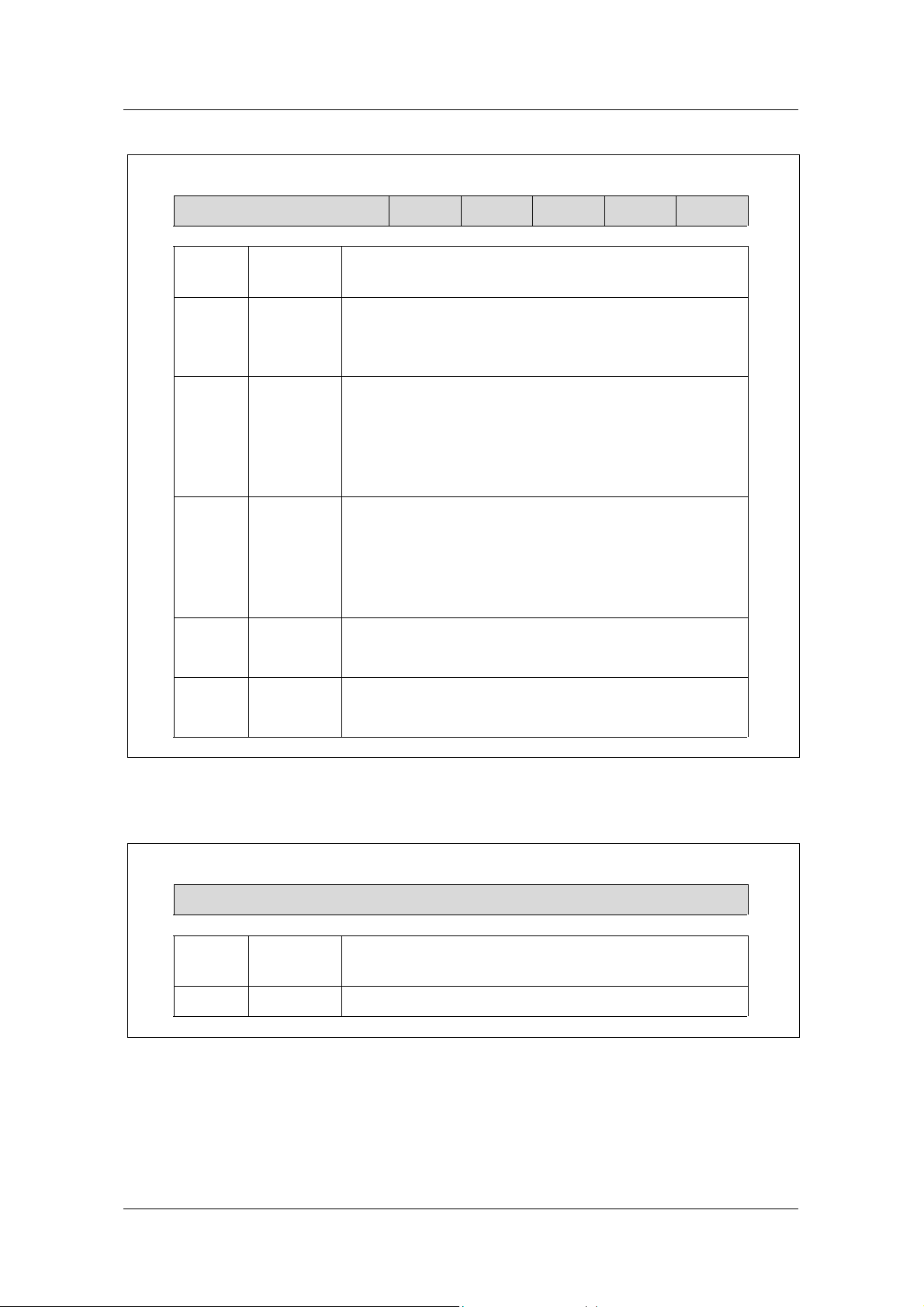
7 6 5 4 3 2 1 0
Reserved I2S PL PB EDAC EADC
Bit
Number
4 I2S I2S Format Enable:
3 PL Polarity of DACLRCK:
4 PB Polarity of DACBCK:
Mnemonic
Bit
Function
When set, I2S format (1 bit delay), When cleared normal
PCM format. Reset value is 0.
When cleared, left channel data is sent through
DACSDATA during LRCK=0. When set, right channel
data is sent through DACSDATA during LRCK=0. Reset
value is 0. (Refer Figure17.)
When cleared, DACSDATA has valid
edges of DACBCK. When set, DACSDATA has valid data
between rising edges of DACBCK. (Refer Figure17.)
Reset value is 0.
1 EDAC External DAC Enable:
When set, external DAC is used. Reset value is 0.
0 EADC External ADC Enable:
When set, external ADC is used. Reset value is 0.
Figure 8. I/O Status reported through HDO3
7 6 5 4 3 2 1 0
Volume
Bit
Number
7:0 Volume
Mnemonic
Bit
The value can be 0 to 200.
Figure 9. Volume reported through HDO4
Function
SAMSUNG Electronics CO. 19/37
Page 20

TL7231MD
7 6 5 4 3 2 1 0
Mode
Bit
Number
0 Mode
7 6 5 4 3 2 1 0
HDO9
HDO8
HDO7
HDO6
Bit
Number
HDO9 7:0
HDO8 7:0
HDO7 7:0
HDO6 7:0
Mnemonic
Figure 10. Serial Interface Mode reported through HDO5
Mnemonic
Figure 11. Count Value reported through HDO6 ~ HDO9
Bit
Bit
Function
Serial Interface Mode.
When set, LSB-first mode. When cleared, MSB-first
mode. The reset value is 0.
Function
These registers show 32-bit unsigned integer value.
HDO9 is the most-significant byte. When mode is 2, it
represents the successfully decoded frame counter
during MP3 decoding. When mode is 3, it represents the
encoded/decoded code count during voice
encoding/decoding.
20/37 SAMSUNG Electronics Co.
Page 21

TL7231MD
7 6 5 4 3 2 1 0
Reserved ID LAYER PT
Bit
Number
3 ID
2:1 LAYER
0 PT
Mnemonic
Figure 12. Frame Header reported through HDO10 when mode is 2.
Bit
Function
0: Reserved
1: ISO/IEC standard 11172-3 audio (MP3)
00: Reserved
01: Layer3
10: Layer2
11: Layer1
TL7231MD decodes only layer3 bit stream.
Protection Bit:
0: CRC Protection
1: No CRC Protection
SAMSUNG Electronics CO. 21/37
Page 22

TL7231MD
7 6 5 4 3 2 1 0
BRI SF PD PR
Bit
Number
7:4 BRI
3:2 SF
1 PD
0 PR
Mnemonic
Figure 13. Frame Header reported through HDO11 when mode is 2.
Bit
Function
Bit Rate Index:
0000: Free
0001: 32Kbps
0010: 40Kbps
0011: 48Kbps
0100: 56Kbps
0101: 64Kbps
0110: 80Kbps
0111: 96Kbps
1000: 112Kbps
1001: 128Kbps
1010: 160Kbps
1011: 192Kbps
1100: 224Kbps
1101: 256Kbps
1110: 320Kbps
1111: Forbidden
Sampling Frequency:
00: 44.1KHz
01: 48KHz
10: 32KHz
11: Reserved
Padding Bit
0: No Padding Bit
1: One Padding Bit
Private Bit
Bit for private use.
22/37 SAMSUNG Electronics Co.
Page 23

TL7231MD
7 6 5 4 3 2 1 0
MODE ME CR OC EM
Bit
Number
7:6 MODE
5:4 ME
3 CR
2 OC
1:0 EM
Mnemonic
Figure 14. Frame Header reported through HDO12 when mode is 2.
Bit
Function
Audio Channel Mode:
00: Stereo
01: Joint Stereo (Intensity Stereo and/or MS Stereo)
10: Dual Channel
11: Single Channel
Joint Stereo Coding Method:
00: Neither Intensity Stereo nor MS Stereo
01: Only Intensity Stereo
10: Only MS Stereo
11: Both Intensity Stereo and MS Stereo
Copyright:
0: No Copyright
1: Copyright Protected
Original/Copy:
0: Copy
1: Original
Type of Deemphasis:
00: None
01: 50/15 microseconds
10: Reserved
11: CCITT J.17
DACDEEM of TL7231MD becomes active if deemphasis
is needed without relation to deemphasis type.
SAMSUNG Electronics CO. 23/37
Page 24

TL7231MD
7 6 5 4 3 2 1 0
CF BB
Bit
Number
7:4 CF
3:0 BB
Figure 15. Bass Boost Information reported through HDO13 when mode is 2.
7 6 5 4 3 2 1 0
Valid
Bit
Number
0 Valid
Mnemonic
Mnemonic
Figure 16. DAC Output Status reported through HDO14
Bit
Bit
Function
Cutoff Frequency:
The value can be in the range of 0 to 6.
Base Boost Value
Function
DAC Output Valid:
When set, output of internal DAC is valid. Reset value is
0.
24/37 SAMSUNG Electronics Co.
Page 25
TL7231MD
DAC
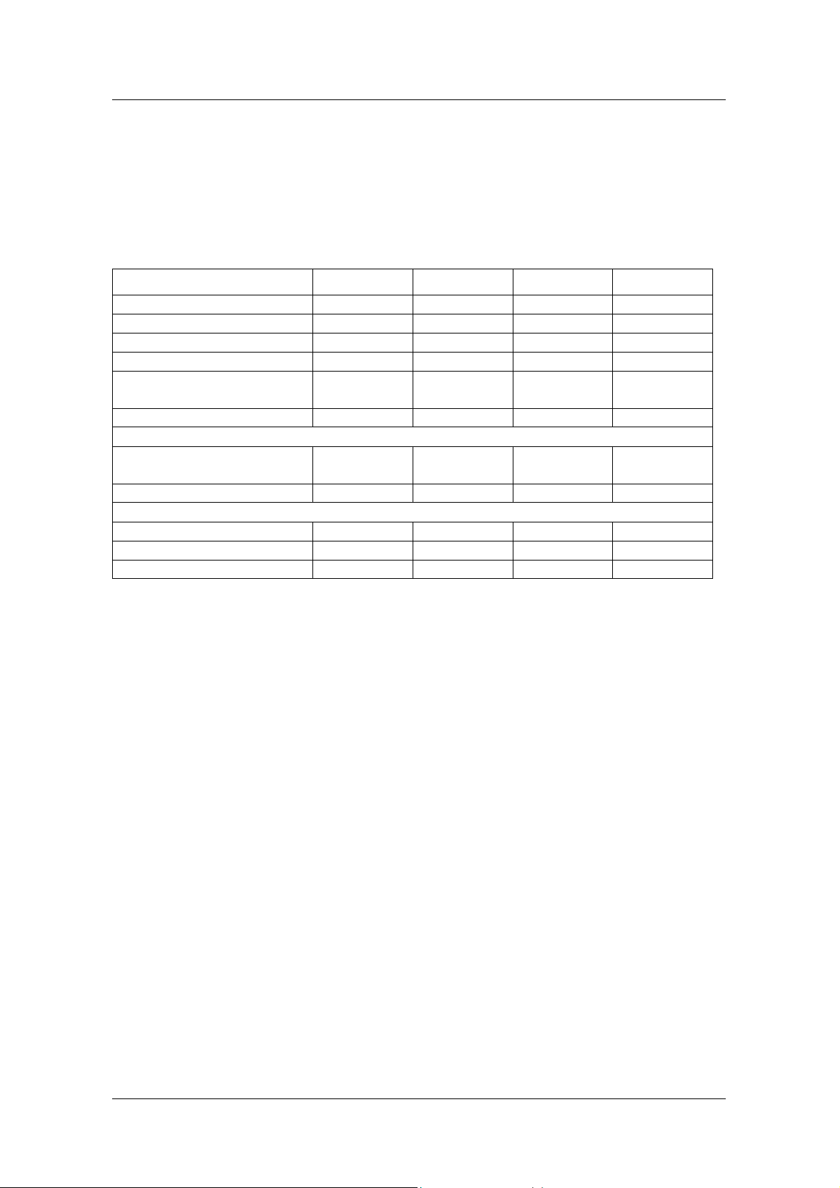
DAC of TL7231MD employs the 1-bit 4th-order sigma-delta architecture with 16-bit resolution,
over-sampling of 64X. Analog post-filter with low clock sensitivity and linear phase can filter out
the shaping-noise and output analog voltage with high resolution. The characteristic of Internal
DAC is shown Table 7.
Table 7. Characteristics of Internal DAC
PARAMETER MIN TYP MAX UNITS
Resolution 16 bits
SNR 79.7 dB
THD 84.9 dB
SNDR 78.5 dB
Reference Voltage Output
(DACVREF)
0.5×
DACVDDA
V
Frequency Response ± 0.1 ± 0.5 dB
Analog Output
Voltage Range 0.5×
Vpp
DACVDDA
Load Impedance 10K Ω
Digital Filter
Pass Band Ripple ± 0.0072 dB
Stop and Attenuation 62.7 dB
Pass Band 0.45 Fs
(DACVDDD/DACVDDA=3.0V, Temp=25°C, Fs=44.1KHz, Signal Freq.=20~20KHz, C
of AOUTL/AOUTR = 10pF)
load
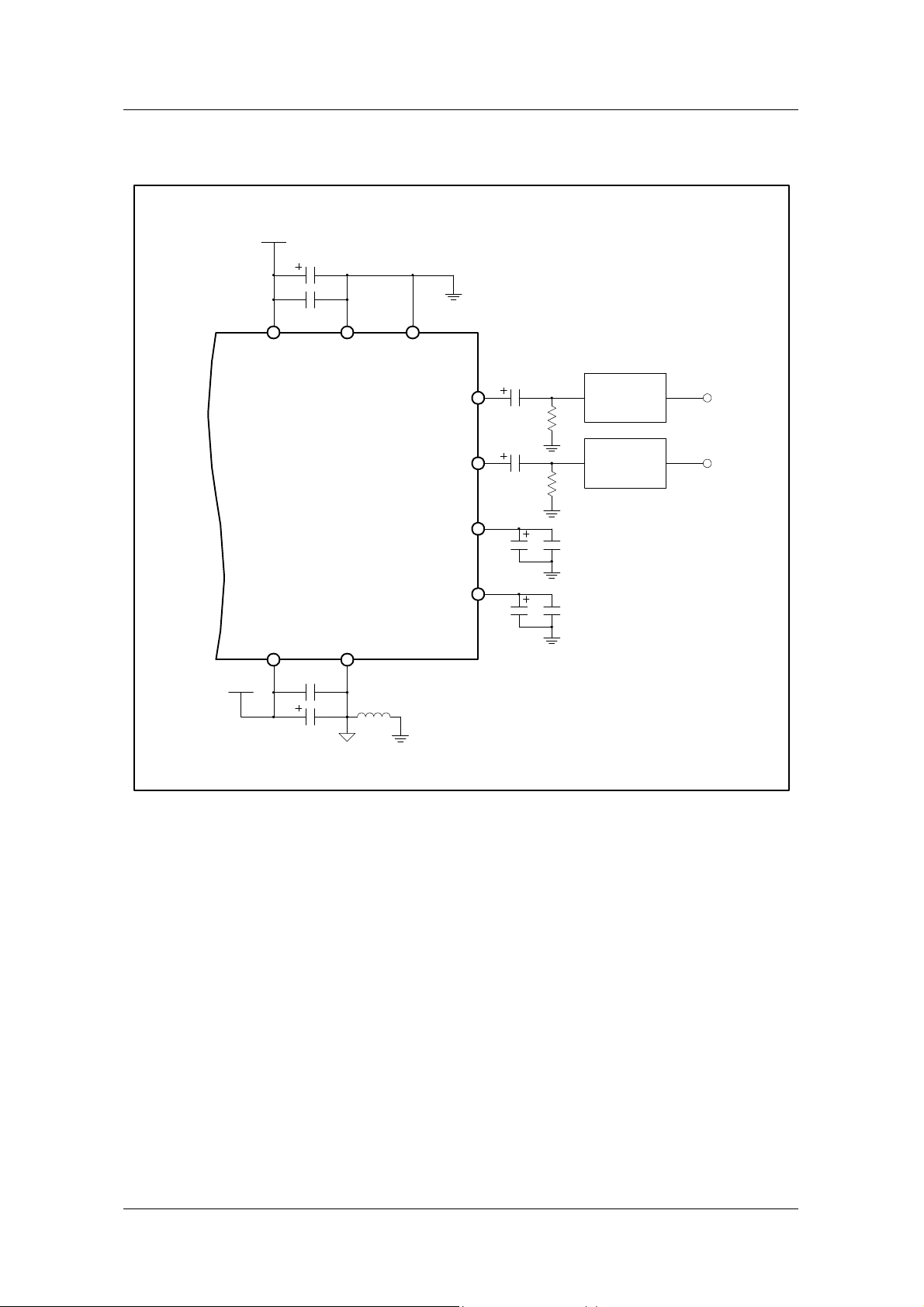
With TL7231MD, user can configure whether the internal DAC is used or not. The configuration
of DAC can be achieved through HIP commands shown in Table 5. When using internal DAC,
the following circuit in Figure 17 is recommended.
SAMSUNG Electronics CO. 25/37
Page 26
TL7231MD
3.0V
10u
0.1u
DACVDDA DACVSSA DACVBB
1u
AOUTR
100K
1u
AOUTL
10u
10u
100K
0.1u
0.1u
TL7231MD
DACVDDD DACVSSD
3.0V
0.1u
10u
DACVREF
DACVHALF
Figure 17. Reference Circuit when using internal DAC
Low Pass
Filter
(optional)
Low Pass
Filter
(optional)
Rout
Lout
26/37 SAMSUNG Electronics Co.
Page 27
TL7231MD
External DAC Interfaces
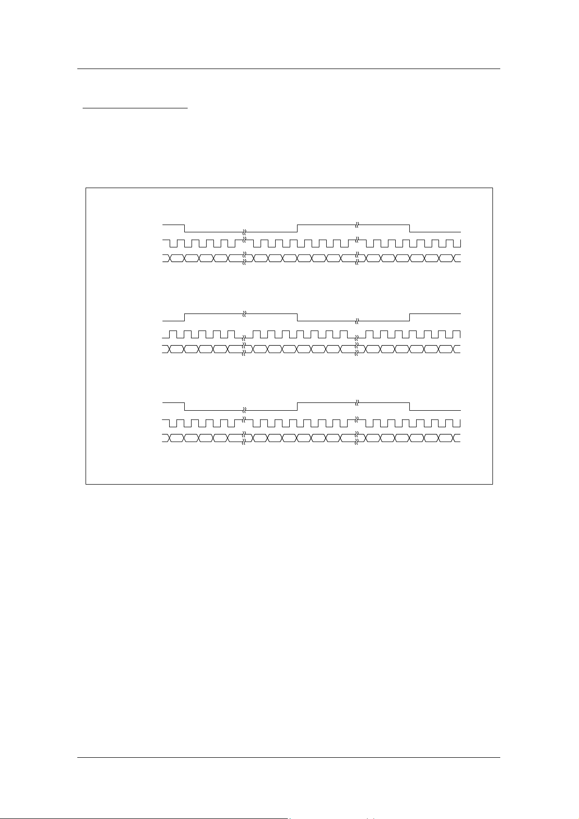
TL7231MD supports eight external interface formats. Three of them, for example, are shown in
Figure 18. The interface can be configured through HIP commands. The frequency of
DACBCLK is 32 times of that of DACLRCK. When voice decoding, only 32KHz of DACLRCK
is used.
Left Channel Right Channel
DACLRCK
DACBCK
DACSDATA
DACLRCK
DACBCK
DACSDATA
MSB-2MSB-1MSB LSB+2 LSB+1 LSB MSB-2MSB-1MSB LSB+2 LSB+1 LSB
Right-Justified Mode
(EDAC: 1, PB: 0, PL: 0, I2S: 0)
Left Channel Right Channel
MSB-2MSB-1MSB LSB+2 LSB+1 LSB MSB-2MSB-1MSB LSB+2 LSB+1 LSB
Right-Justified Mode
(EDAC: 1, PB: 1, PL: 1, I2S: 0)
DACLRCK
DACBCK
DACSDATA
Left Channel Right Channel
MSB-1MSB LSB+2 LSB+1 LSB MSB-1MSB LSB+2 LSB+1 LSB
I2S-Justified Mode
(EDAC: 1, PB: 0, PL: 0, I2S: 1)
Figure 18. Examples of External DAC Interfaces
SAMSUNG Electronics CO. 27/37
Page 28
TL7231MD
ADC
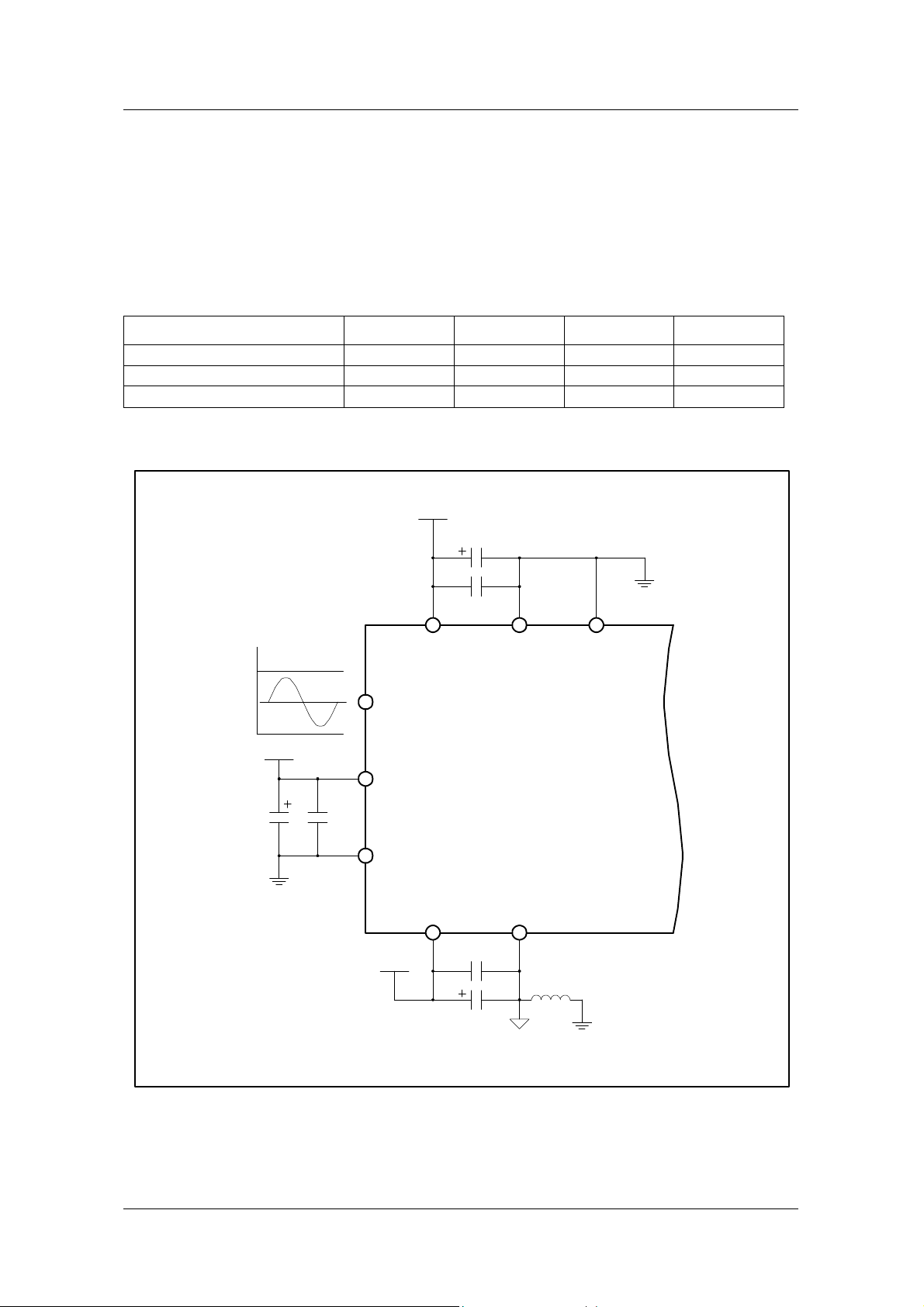
The internal ADC of TL7231MD is 12-bit resolution ADC. It is recycling type ADC with sampleand-hold function. The analog input ADCAIN should be single-ended type with the range from
ADCREFP to ADCREFN. This ADCAIN voltage follows reference voltage range fundamentally.
So, if user wants to alter the input range, the voltage value of ADCREFP should be changed.
But ADCREFP should be greater than 2.0V. The characteristic of internal ADC is shown Table 8.
Table 8. Characteristics of Internal ADC
PARAMETER MIN TYP MAX UNITS
THD 74.3 dB
SNR 64.9 dB
SNDR 64.4 dB
(ADCVDDD/ADCVDDA=3.0V, ADCAIN=8KHz)
3.0V
10u
ADCREFP
ADCREFP/2
ADCREFN
Vref
10u 0.1u
0.1u
ADCVDDA ADCVSSA ADCVBB
ADCAIN
ADCREFP
ADCREFN
ADCVDDD ADCVSSD
3.0V
TL7231MD
0.1u
10u
Figure 19. Reference Circuit when using internal ADC
With TL7231MD, the following circuit in Figure 19 is recommended to use internal ADC.
28/37 SAMSUNG Electronics Co.
Page 29
TL7231MD
Voice Record/Playback Function
TL7231MD records voice data from ADC in 8kHz sampling rate. There are three compression
modes according to bit rates of compressed data: high quality (32Kbps), medium quality
(24Kbps) and low quality (16Kbps). In high quality mode, relatively large bits are allocated for
compressed data to achieve high quality of the sound. In low quality mode, smaller bits are
allocated to record much more samples in the same size of storage media. Medium quality
mode gives tradeoff between high and low quality modes. Compressed codes are byte-aligned
and transmitted to host MCU through the serial port.
In playback the codes are uncompressed to PCM samples, with the compression mode in
recording, and then oversampled to 32 kHz and output to DAC. Compressed codes are
transmitted from host MCU through the serial interface.
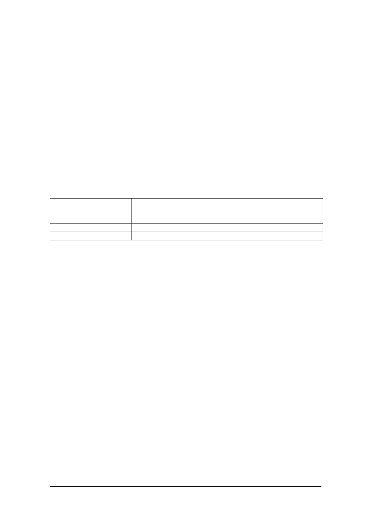
Table 9 is the summary of the relation between compression modes and code size.
Table 9. Summary of Three Voice Compression Modes
COMPRESSION MODES CODE LENGTH
High Quality (32Kbps) 4 140 min.
Medium Quality (24Kbps) 3 186 min.
Low Quality (16Kbps) 2 280 min.
(BIT)
RECORDING TIME
FOR 32MB STORAGE MEDIA
SAMSUNG Electronics CO. 29/37
Page 30

TL7231MD
Lower Power Operation
TL7231MD has low-power feature that makes the processor get into very low-power dormant
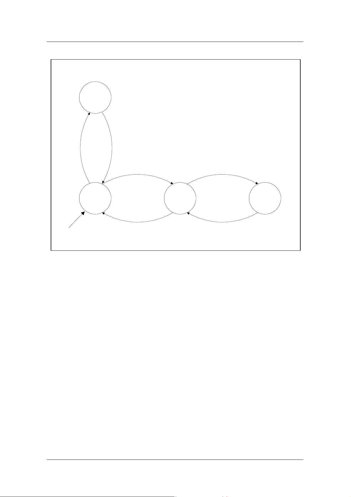
states through hardware or software control. The power saving scheme is explained with the
state diagram of TL7231MD shown in Figure 20.
RUN
In this state, TL7231MD decodes MP3 or compressed voice bit stream, or encodes voice signal.
Also in this state it can process other HIP commands such as 20h and 21h. HIP command 01h,
04h through 09h, and 0Fh should not be used in this state. TL7231MD consumes normal power
at this state, It processes all internal functions and drives external pads. It can transit to WAIT
state with HIP command 00h. When there is no job left or it waits available data, power
consumption is reduced as that of WAIT state.
WAIT
When RESET signal becomes active, TL7231MD goes into WAIT state. There it can transit to
RUN, or SLEEP state. When TL7231MD is in this state, it is ready to receive any HIP
commands from host. It can go into RUN state when it receives HIP commands such as 01h,
04h though 09h. Also it can process other HIP commands such as volume control (21h) etc. in
this state. TL7231MD goes into this state through HIP command 00h from RUN state. When
TL7231MD is in this state, only peripheral interface block consumes power. That is, internally
generated peripheral clock is active but clock for the DSP core logic is not. When it receives HIP
command 0Fh, it goes into SLEEP state in which more power is saved.
SLEEP
In SLEEP state, only internal analog blocks such as PLL, ADC and DAC of TL7231MD
consume power. In this state, internal ADC and DAC are disabled. But PLL consumes normal
operation power. In this state, TL7231MD can transit to PWRDOWN state when external
PWRDN pin becomes active. Active WAKEUP signal changes its state from SLEEP to WAIT.
PWRDOWN
When TL7231MD is in SLEEP state and PWRDN signal becomes active, it transits to
PWRDOWN. To make TL7231MD stay in this state, the external PWRDN signal keep its active
state. When the PWRDN signal becomes inactive, TL7231MD exits from this PWRDOWN state,
and then goes into SLEEP state. When it changes its state from PWRDOWN to SLEEP, this
state should not be changed during minimum 150µs until internal PLL is stabilized. TL7231MD
consumes the minimum power at this state because all internal logic blocks and analog blocks
are power-downed.
30/37 SAMSUNG Electronics Co.
Page 31
RUN
(00h)
TL7231MD
HIP COMMAND
RESET
WAIT
HIP COMMAND
HIP COMMAND
(0Fh)
PWRDN PIN
SLEEP
WAKEUP PIN
PWRDN PIN
Figure 20. Decoder States and Power Management
PWR-
DOWN
SAMSUNG Electronics CO. 31/37
Page 32
TL7231MD
ELECTRICAL SPECIFICATIONS
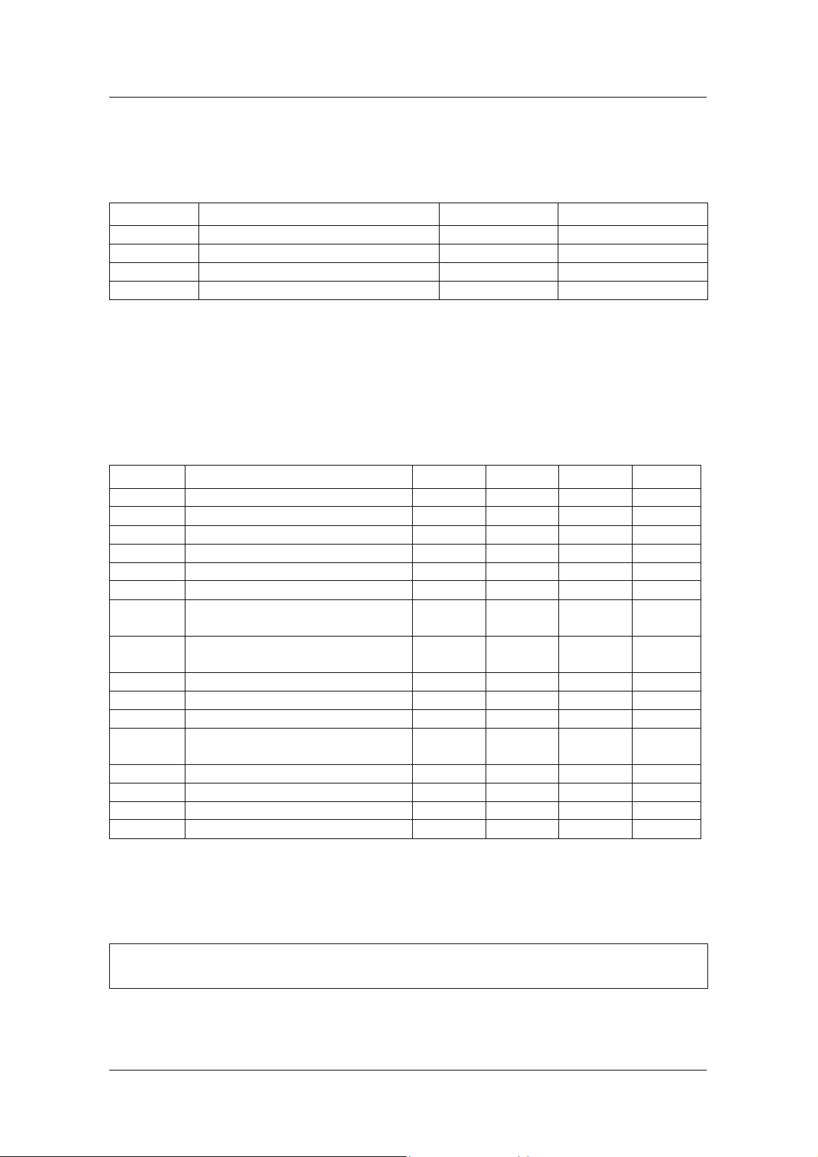
ABSOLUTE MAXIMUM RATINGS (See Notes)†
Symbol Parameter Rating Unit
VDD DC Supply Voltage -0.3 to 3.8 V
VIN DC Input Voltage -0.3 to 5.5 V
IIN DC Input Current ± 10 mA
T
Storage Temperature -40 to 125 °C
STG
† Stresses beyond those listed under “ absolute maximum ratings” may cause permanent damage to the device. These
are stress ratings only, and functional operation of the device at these or any other conditions beyond those indicated
under “ DC ELECTRICAL CHARACTERISTICS” is not implied. Exposure to absolute-maximum-rated conditions for
extended periods may affect device reliability.
NOTE 1: All voltage values are with respect to VSS.
NOTE 2: This value was obtained under specially produced worst-case test conditions for the TL7231MD, which are
not sustained during normal device operation.
DC ELECTRICAL CHARACTERISTICS (Note3)†
Symbol Parameter MIN TYP MAX UNIT
VDD Supply voltage 2.7 3.0 3.3 V
VSS Supply voltage 0 V
VIH High level input voltage 1.8 V
VIL Low level input voltage -0.3 0.6 V
V
High level output voltage 2 V
OH
V
Low level output voltage 0.4 V
OL
High level input leakage current
without internal pull-up
Low level input leakage current
without internal pull-up
-10 +10 µA
-10 +10 µA
Supply current in RUN state 61 mA
Supply current in WAIT state 26 mA
Supply current in SLEEP 12 mA
Supply current in PWRDOWN
state
250 µA
Input capacitance 4 pF
Output capacitance 4 pF
C
I
C
I
I
WT
I
I
IH
I
IL
RN
SL
PD
IN
OUT
TA Air temperature -40 85 °C
V
High level input voltage for CPUXI
CPUXI
† For TL7231MD, all typical values are at VDD = 3.0 V, TA (air temperature) = 25°C.
2.5 V
NOTE 3: All voltage values are with respect to VSS. All input and output voltage levels are TTL-compatible. CLKIN can
be driven by CMOS clock.
DD
DD
+0.3
+0.3
V
V
NOTICE: This document contains information on products in the sampling and initial production
phases of development. The specifications are subject to change without notice.
32/37 SAMSUNG Electronics Co.
Page 33
TL7231MD
AC ELECTRICAL CHARACTERISTICS
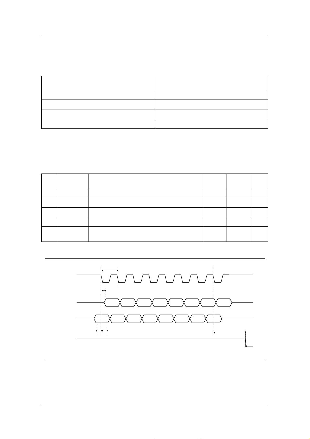
AC Test Condition
Parameter Value
Temperature 85°C
Supply Voltage 3.0V
Input Rise and Fall Times 2ns
Output Load 10pF
Serial port
The following table defines the timing parameters for the serial port pins. The numbers shown in
Figure 21 correspond to each number in the first column of the table.
NO. Symbol Description MIN MAX Unit
1 TCC Cycle time of CLKXRM 144.7 ns
2 TD Delay time, CLKXRM to DXRM valid 42.2 78.4 ns
3 TSU Setup time, DXRM before CLKXRM low 1.9 ns
4 TH Hold time, DXRM from CLKXRM low 1.2 ns
5 T
REQ
Request check time, falling edge of CLKXRM
to falling edge of REQSTRM
295.2 331.3 ns
1
CLKXRM
2
DXRM
(Transmit)
DXRM
(Receive)
Bit0 Bit1 Bit2 Bit3 Bit4 Bit5 Bit6 Bit7
Bit0 Bit1 Bit2 Bit3 Bit4 Bit5 Bit6 Bit7
3 4
5
REQSTRM
Figure 21. Timing for Serial Port in case of LSB-First Mode
SAMSUNG Electronics CO. 33/37
Page 34
TL7231MD
Host interface Port
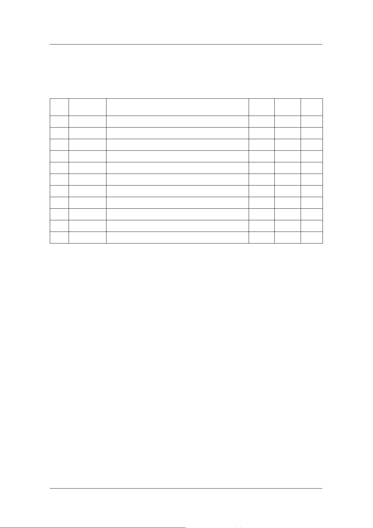
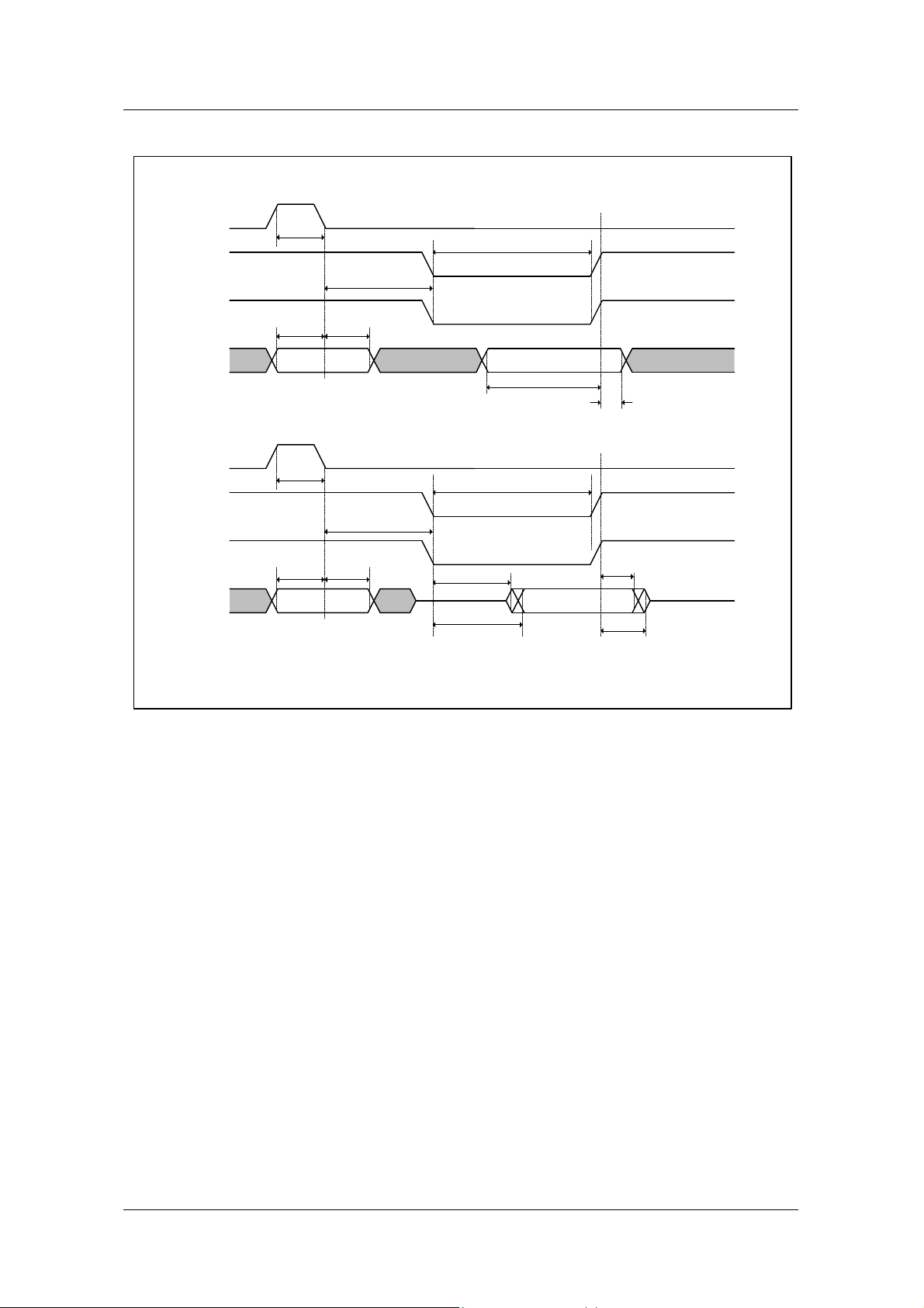
The following table defines the timing parameters for the Host Interface Port I/O pins. The
numbers shown in Figure 22 correspond to each number in the first column of the table.
NO. Symbol Description MIN MAX Unit
6 T
7 T
8 T
9 T
10 T
11 T
12 T
13 T
14 T
15 T
16 T
HALE pulse width 2.0 ns
HAW
Setup time, HD address setup before HALE low 2.0 ns
HDSU
Hold time, HD address hold after HALE low 0.8 ns
HDH
Start of write or read after HALE low 0.0 ns
HAS
Setup time, HD data setup before end of write 0.7 ns
HDSU
Hold time, HD data hold after end of write 2.2 ns
HDH
Read or write pulse width 36.2 ns
HRW
HD data enabled after start of read 7.8 ns
HDE
HD data valid after start of read 7.9 ns
HDD
HD data hold after end of read 3.7 7.8 ns
HRDH
HD data disabled after end of read 4.2 7.9 ns
HRDD
34/37 SAMSUNG Electronics Co.
Page 35
TL7231MD
HALE
HSEL#
HWR#
HD[7:0]
HALE
HSEL#
HRD#
HD[7:0]
6
9
7 8
12
DATAADDRESS
10
HOST Write Cycle
5
9
7 8
ADDRESS DATA
12
13
14
HOST Read Cycle
11
15
16
Figure 22. Timing for Host Interface Port pins
SAMSUNG Electronics CO. 35/37
Page 36
TL7231MD
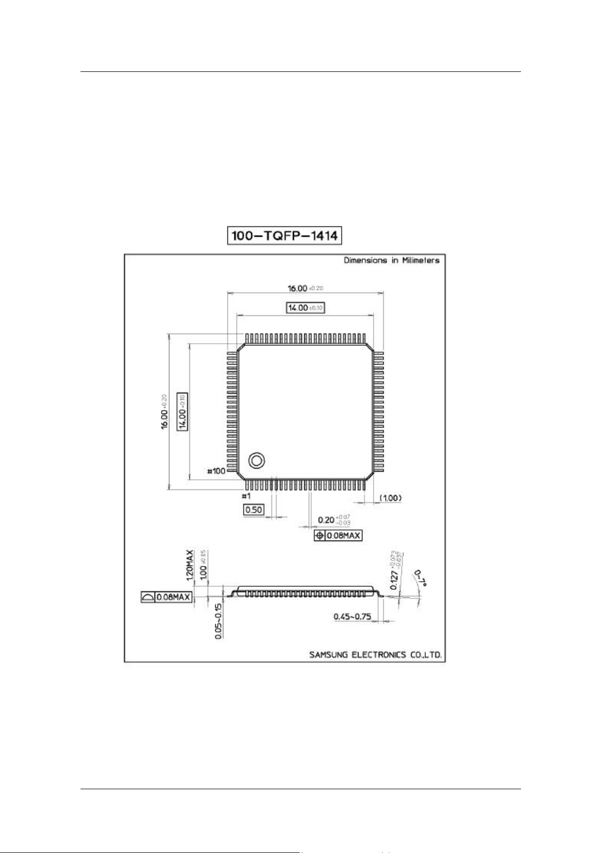
PACKAGE DIMENSION
36/37 SAMSUNG Electronics Co.
Page 37

TL7231MD
The reproduction of this datasheet is NOT allowed without approval of SEC.
All information and data contained in this datasheet are subject to change without notice. This
publication supersedes and replaces all information previously supplied. SEC has no
responsibility to the consequence of using the patents described in this document.
© 1999 SAMSUNG Electronics Co., – All Rights Reserved
SAMSUNG Electronics CO. 37/37
 Loading...