

TL7700
SUPPLY-VOLTAGE SUPERVISOR
SLVS220A – JULY 1999 – REVISED NOVEMBER 1999
1
POST OFFICE BOX 655303 • DALLAS, TEXAS 75265
D
Adjustable Sense Voltage With Two
External Resistors
D
Adjustable Hysteresis of Sense Voltage
D
Wide Operating Supply-Voltage
Range . . . 1.8 V to 40 V
D
Wide Operating-Temperature
Range ...–40°C to 85°C
D
Low Power Consumption (ICC = 0.6 mA
TYP, VCC = 40 V)
D
Minimum External Components
D
Package Options Include Plastic
Small-Outline (PS) and Thin Shrink
Small-Outline (PW) Packages and Standard
DIP (P)
description
The TL7700 is a bipolar integrated circuit designed for use as a reset controller in microcomputer and
microprocessor systems. The SENSE voltage can be set to any value greater than 0.5 V using two external
resistors. The hysteresis value of the sense voltage also can be set by the same resistors. The device includes
a precision voltage reference, fast comparator, timing generator, and output driver, so it can generate a
power-on reset signal in a digital system.
The TL7700 has an internal 1.5-V temperature-compensated voltage reference from which all function blocks
are supplied. Circuit function is very stable, with supply voltage in the 1.8-V to 40-V range. Minimum supply
current allows use with ac line operation, portable battery operation, and automotive applications.
The TL7700C is characterized for operation from –40°C to 85°C.
AVAILABLE OPTIONS
PACKAGED DEVICES
T
A
PLASTIC
DIP
(P)
PLASTIC
SMALL OUTLINE
(PS)
PLASTIC
THIN SHRINK
SMALL OUTLINE
(PW)
–40°C to 85°C TL7700CP TL7700CPS TL7700CPW
PS and PW packages are available taped and reeled. Add the suffix R to device type
(e.g., TL7700CPSR).
Copyright 1999, Texas Instruments Incorporated
PRODUCTION DATA information is current as of publication date.
Products conform to specifications per the terms of Texas Instruments
standard warranty. Production processing does not necessarily include
testing of all parameters.
Please be aware that an important notice concerning availability, standard warranty, and use in critical applications of
Texas Instruments semiconductor products and disclaimers thereto appears at the end of this data sheet.
1
2
3
4
8
7
6
5
CT
SENSE
NC
GND
RESET
NC
NC
V
CC
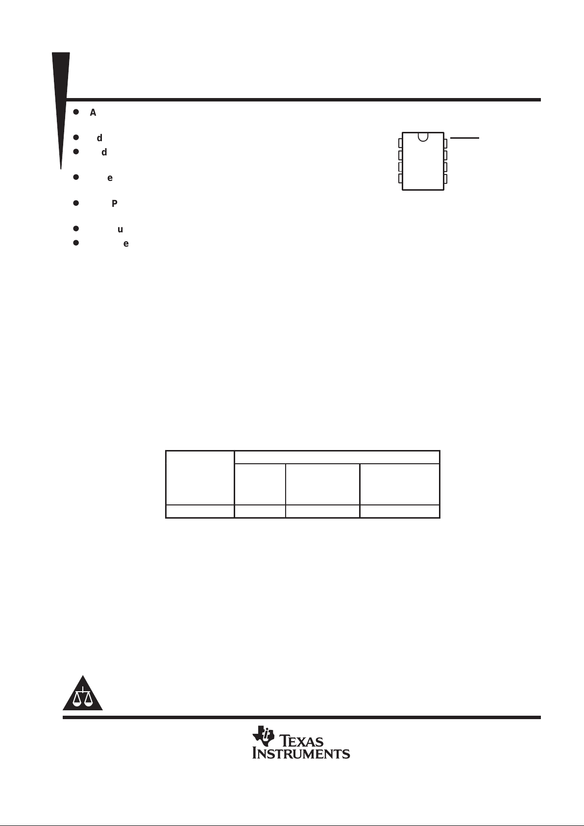
P, PS, OR PW PACKAGE
(TOP VIEW)
NC – No internal connection
TL7700
SUPPLY-VOLTAGE SUPERVISOR
SLVS220A – JULY 1999 – REVISED NOVEMBER 1999
2
POST OFFICE BOX 655303 • DALLAS, TEXAS 75265
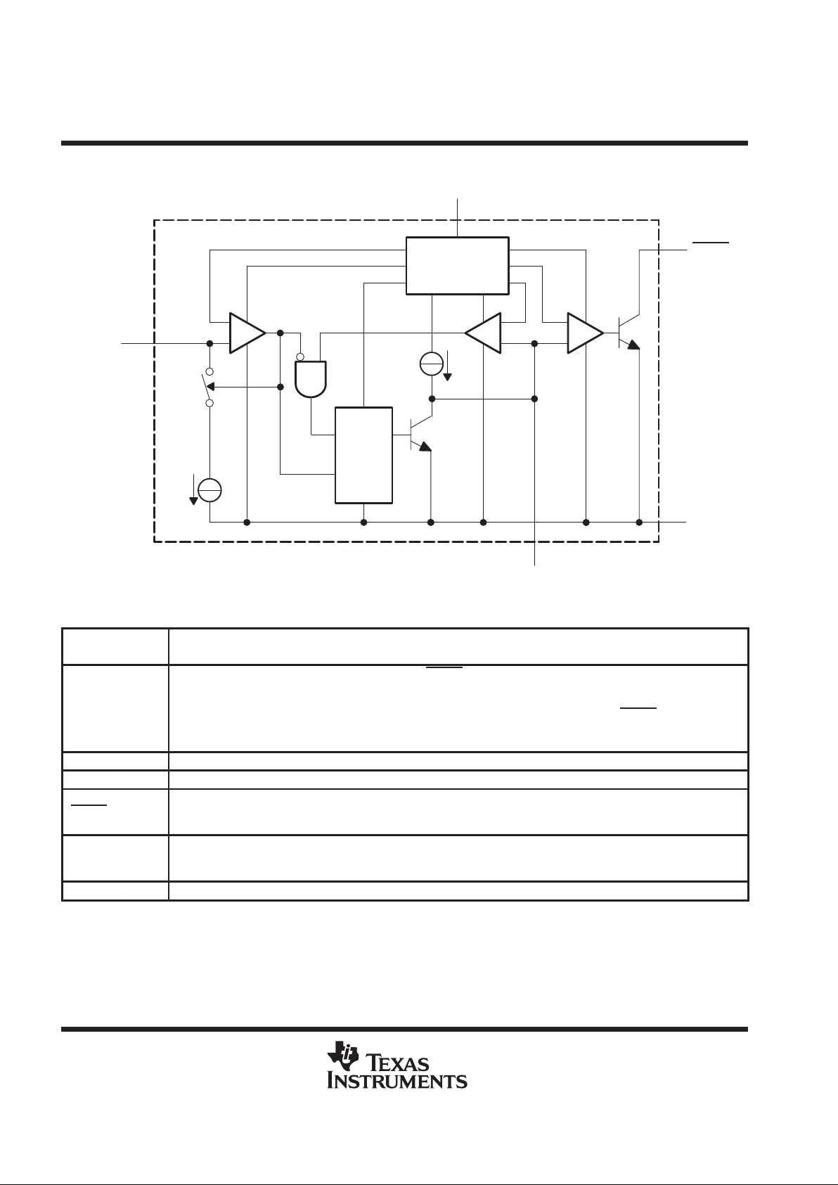
functional block diagram
Reference
Voltage
+
–
+
–
R
S
Q
+
–
Vs = 500 mV TYP
RESET
GND
CT
SENSE
†
ICT = 15 µA TYP; Is = 2.5 µA TYP
V
CC
I
CT
†
High:
On
I
S
†
Terminal Functions
TERMINAL
NAME NO.
DESCRIPTION
CT 1
Timing capacitor connection. This terminal sets the RESET output pulse duration (tpo). It is connected internally to a
15-µA constant-current source. There is a limit on the switching speed of internal elements; even if CT is set to 0,
response speeds remain at approximately 5 to 10 µs. If CT is open, the device can be used as an adjustable-threshold
noninverting comparator . If CT is low, the internal output-stage comparator is active and the RESET
output transistor
is on. An external voltage must not be applied to this terminal due to the internal structure of the device. Therefore, drive
the device using an open-collector transistor, FET, or 3-state buffer (in the low-level or high-impedance state).
GND 4 Ground. Keep this terminal as low impedance to reduce circuit noise.
NC 3, 6, 7 No internal connection
RESET 8
Reset output. This terminal can be connected directly to a system that resets in the active-low state. A pullup resistor
usually is required because the output is an npn open-collector transistor. An additional transistor should be connected
when the active-high reset or higher output current is required.
SENSE 2
Voltage sense. This terminal has a threshold level of 500 mV. The sense voltage and hysteresis can be set at the same
time when the two voltage-dividing resistors are connected. The reference voltage is temperature compensated to inhibit
temperature drift in the threshold voltage within the operating temperature range.
V
CC
5 Power supply. This terminal is used in an operating-voltage range of 1.8 V to 40 V.
TL7700
SUPPLY-VOLTAGE SUPERVISOR
SLVS220A – JULY 1999 – REVISED NOVEMBER 1999
3
POST OFFICE BOX 655303 • DALLAS, TEXAS 75265
absolute maximum ratings over operating free-air temperature range (unless otherwise noted)
†
Supply voltage, VCC (see Note 1) 41 V. . . . . . . . . . . . . . . . . . . . . . . . . . . . . . . . . . . . . . . . . . . . . . . . . . . . . . . . . . . .
Sense input voltage range, Vs –0.3 V to 41 V. . . . . . . . . . . . . . . . . . . . . . . . . . . . . . . . . . . . . . . . . . . . . . . . . . . . . .
Output voltage, VOH (off state) 41 V. . . . . . . . . . . . . . . . . . . . . . . . . . . . . . . . . . . . . . . . . . . . . . . . . . . . . . . . . . . . . .
Output current, I
OL
(on state) 5 mA. . . . . . . . . . . . . . . . . . . . . . . . . . . . . . . . . . . . . . . . . . . . . . . . . . . . . . . . . . . . . . .
Package thermal impedance, θJA (see Notes 2 and 3): P package 85°C/W. . . . . . . . . . . . . . . . . . . . . . . . . . . .
PS package 95°C/W. . . . . . . . . . . . . . . . . . . . . . . . . . .
PW package 149°C/W. . . . . . . . . . . . . . . . . . . . . . . . .
Storage temperature range, T
stg
–65°C to 150°C. . . . . . . . . . . . . . . . . . . . . . . . . . . . . . . . . . . . . . . . . . . . . . . . . . .
†
Stresses beyond those listed under “absolute maximum ratings” may cause permanent damage to the device. These are stress ratings only, and
functional operation of the device at these or any other conditions beyond those indicated under “recommended operating conditions” is not
implied. Exposure to absolute-maximum-rated conditions for extended periods may affect device reliability.
NOTES: 1. All voltage values are with respect to the network ground terminal.
2. Maximum power dissipation is a function of TJ(max), θJA, and TA. The maximum allowable power dissipation at any allowable
ambient temperature is PD = (TJ(max) – TA)/θJA. Operating at the absolute maximum TJ of 150°C can impact reliability.
3. The package thermal impedance is calculated in accordance with JESD 51.
recommended operating conditions
MIN NOM MAX UNIT
Supply voltage, V
CC
1.8 40 V
Low-level output current, I
OL
3 mA
Operating free-air temperature, T
A
–40 85 °C
electrical characteristics, VCC = 3 V, TA = 25°C (unless otherwise noted)
PARAMETER
TEST CONDITIONS
MIN TYP MAX UNIT
p
495 500 505
VsSENSE input voltage
TA = –40°C to 85°C 490 510
mV
p
2 2.5 3
IsSENSE input current
V
s
= 0.4
V
TA = –40°C to 85°C 1.5 3.5
µ
A
I
CC
Supply current VCC = 40 V, Vs = 0.6 V, No load 0.6 1 mA
p
IOL = 1.5 mA 0.4
VOLLow-level output voltage
IOL = 3 mA 0.8
V
I
OH
High-level output current VOH = 40 V, Vs = 0.6 V, TA = –40°C to 85°C 1 µA
I
CT
Timing-capacitor charge current Vs = 0.6 V 11 15 19 µA
switching characteristics, VCC = 3 V, TA = 25°C (unless otherwise noted)
PARAMETER TEST CONDITIONS MIN TYP MAX UNIT
t
pi
SENSE pulse duration CT = 0.01 µF 2 µs
t
po
Output pulse duration CT = 0.01 µF 0.5 1 1.5 ms
t
r
Output rise time CT = 0.01 µF, RL = 2.2 kΩ, CL = 100 pF 15 µs
t
f
Output fall time CT = 0.01 µF, RL = 2.2 kΩ, CL = 100 pF 0.5 µs
t
pd
Propagation delay time, SENSE to output CT = 0.01 µF 10 µs
TL7700
SUPPLY-VOLTAGE SUPERVISOR
SLVS220A – JULY 1999 – REVISED NOVEMBER 1999
4
POST OFFICE BOX 655303 • DALLAS, TEXAS 75265
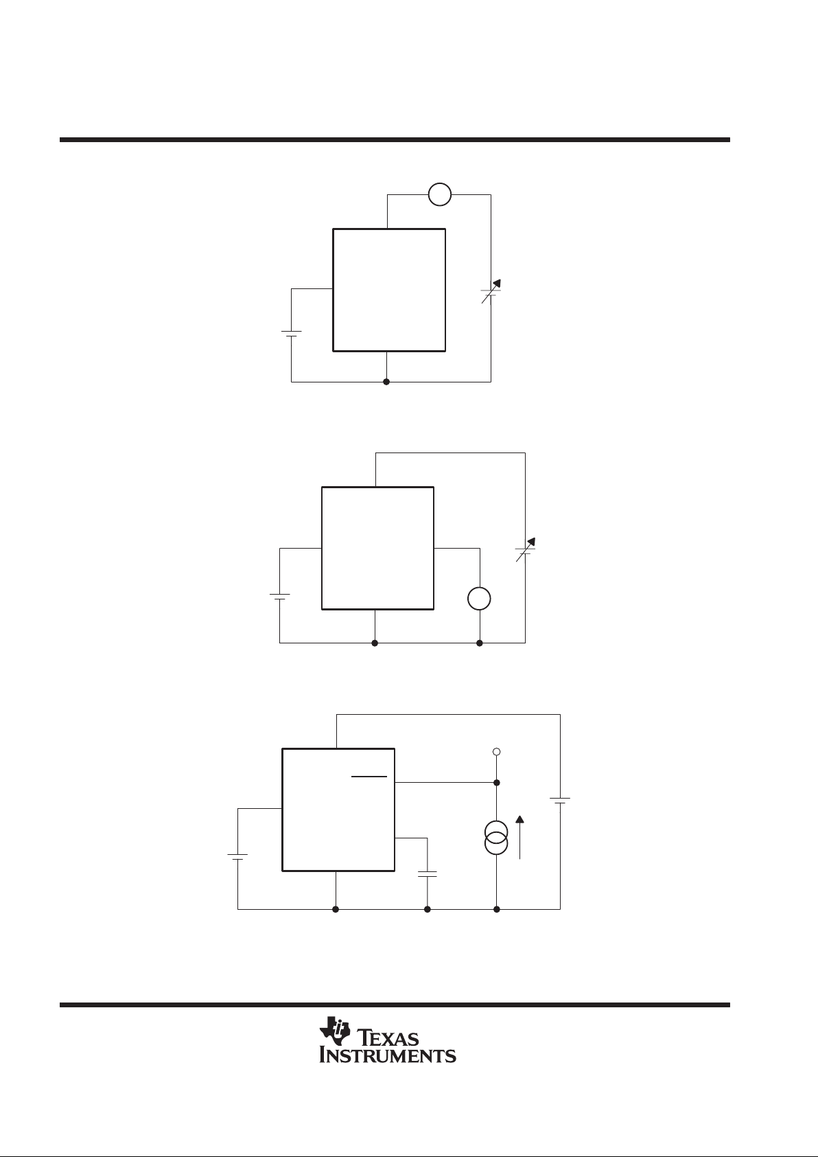
PARAMETER MEASUREMENT INFORMATION
V
CC
V
CC
V
s
GND
0.6 V
SENSE
A
+–
Figure 1. VCC vs ICC Measurement Circuit
V
CC
V
CC
V
s
GND
0.6 V
CTSENSE
A
+
–
Figure 2. VCC vs I
CT
0.4 V
V
CC
V
s
GND
3 V
CT
RESET
0.01 µF
Test
Point
SENSE
Figure 3. I
OL
vs V
OL

TL7700
SUPPLY-VOLTAGE SUPERVISOR
SLVS220A – JULY 1999 – REVISED NOVEMBER 1999
5
POST OFFICE BOX 655303 • DALLAS, TEXAS 75265
PARAMETER MEASUREMENT INFORMATION
V
s
V
CC
V
s
GND
V
CC
CT
RESET
2.2 kΩ
0.01 µF
Test
Point
SENSE
A
+–
Figure 4. VS, IS Characteristics
V
CC
V
s
GND
3 V
CT
2.2 kΩ
100 pF
Test
Point
C
t
RESET
SENSE
Figure 5. Switching Characteristics

TL7700
SUPPLY-VOLTAGE SUPERVISOR
SLVS220A – JULY 1999 – REVISED NOVEMBER 1999
6
POST OFFICE BOX 655303 • DALLAS, TEXAS 75265
TYPICAL CHARACTERISTICS
†
Figure 6
0 102030 405060
0
0.2
0.4
0.6
0.8
1.0
1.2
TA = 85_C
TA = 25_C
TA = –40_C
VCC – Supply Voltage – V
I
CC
– Supply Current – mA
SUPPLY CURRRENT
vs
SUPPLY VOLTAGE
Figure 7
0 102030 405060
10
11
12
13
14
15
16
VCC – Supply Voltage – V
Timing-Capacitor Charge Current Supply – mV
TA = 85_C
TA = 25_C
TA = –40_C
TIMING-CAPACITOR CHARGE CURRENT
vs
SUPPLY VOLTAGE
Figure 8
0123456
0
0.2
0.4
0.6
0.8
1.0
1.2
IOL – Low-Level Output Current – mA
V
OL
– Low-Level Output Voltage – V
TA = 85_C
TA = 25_C
TA = –40_C
V
OL
vs
I
OL
Figure 9
–75
488
490
492
494
496
498
500
502
504
506
–50 –25 0 25 50 75 100 125 150
TA – Free-Air Temperature – °C
TA = 25_C
VS = 500.8 mV
TA = 25_C
VS = 498.3 mV
V
s
– Sense Input Voltage – mV
SENSE INPUT VOLTAGE
vs
TEMPERATURE
†
Data at high and low temperatures are applicable only within the recommended operating conditions.

TL7700
SUPPLY-VOLTAGE SUPERVISOR
SLVS220A – JULY 1999 – REVISED NOVEMBER 1999
7
POST OFFICE BOX 655303 • DALLAS, TEXAS 75265
TYPICAL CHARACTERISTICS
†
Figure 10
–75
1.6
1.8
2.0
2.2
2.4
2.6
2.8
3.0
3.2
3.4
–50 –25 0 25 50 75 100 125 150
TA – Free-Air Temperature – °C
I
s
– Sense Input Current –
µ
A
SENSE INPUT CURRENT
vs
TEMPERATURE
Figure 11
0
–1.0
–0.5
0
0.5
1.0
1.5
2.0
2.5
3.0
3.5
0.1 0.2 0.3 0.4 0.5 0.6 1.0 10 40
Vs – Sense Input Voltage – V
I
s
– Sense Input Current –
µ
A
SENSE INPUT CURRENT
vs
SENSE INPUT VOLTAGE
1
1
10
1
10
2
10
3
10
4
10
5
10
6
10
7
10
8
10
9
10110210310410510610710810
9
t
po
– Output Pulse Duration –
µ
s
Ct – Timing Capacitor – pF
OUTPUT PULSE DURATION
vs
TIMING CAPACATOR
Figure 12
†
Data at high and low temperatures are applicable only within the recommended operating conditions.

TL7700
SUPPLY-VOLTAGE SUPERVISOR
SLVS220A – JULY 1999 – REVISED NOVEMBER 1999
8
POST OFFICE BOX 655303 • DALLAS, TEXAS 75265
TYPICAL CHARACTERISTICS
Figure 13. VCC vs Output Test Circuit 1
V
CC
V
s
GND
CT
RESET
2.2 kΩ
30 kΩ
510 pF
Test
Point 1
240 kΩ
100 pF
Test
Point 2
6 V
SENSE
Figure 14. VCC vs Output Waveform 1
X-Axis = 0.2 ms/Division
TP1
TP2
Y-Axis (TP1) = 1 V/Division
Y-Axis (TP2) = 2 V/Division
Figure 15. VCC vs Output Test Circuit 2
V
CC
V
s
GND
CT
RESET
2.2 kΩ
30 kΩ
510 pF
Test
Point 1
240 kΩ
100 pF
Test
Point 2
6 V
SENSE
TP2
Figure 16. VCC vs Output Waveform 2
X-Axis = 0.2 ms/Division
TP1
Y-Axis (TP1) = 1 V/Division
Y-Axis (TP2) = 2 V/Division

TL7700
SUPPLY-VOLTAGE SUPERVISOR
SLVS220A – JULY 1999 – REVISED NOVEMBER 1999
9
POST OFFICE BOX 655303 • DALLAS, TEXAS 75265
TYPICAL CHARACTERISTICS
Figure 17. VCC vc Output Test Circuit 3
V
CC
V
s
GND
CT
RESET
2.2 kΩ
30 kΩ
510 pF
Test
Point 1
240 kΩ
100 pF
Test
Point 2
SENSE
Figure 18. VCC vs Output Waveform 3
X-Axis = 0.2 ms/Division
TP1
TP2
Y-Axis (TP1) = 1 V/Division
Y-Axis (TP2) = 2 V/Division
detailed description
sense-voltage setting
The sense voltage, V
s
, of the TL7700 typically is 500 mV. By using two external resistors, the circuit designer
can obtain any sense voltage over 500 mV. In Figure 19, the sensing voltage, V′s, is calculated as:
V′s = Vs × (R1 + R2)/R2
Where:
Vs = 500 mV, typically at TA = 25°C
At room temperature, Vs has a variation of 500 mV ± 5 mV. In the basic circuit shown in Figure 19, variations
of [±5 × (R1 + R2)/R2] mV are superimposed on Vs.
V
CC
V
s
GND
CT
RESET
R
L
R1
R2
C
t
V
CC
RESET
GND
SENSE
Figure 19

TL7700
SUPPLY-VOLTAGE SUPERVISOR
SLVS220A – JULY 1999 – REVISED NOVEMBER 1999
10
POST OFFICE BOX 655303 • DALLAS, TEXAS 75265
sense-voltage hysteresis setting
If the sense voltage, V
s
, does not have hysteresis in it and the voltage on the sensing line contains ripples, the
resetting of TL7700 will be unstable. Hysteresis is added to the sense voltage to prevent such problems. As
shown in Figure 20, the hysteresis, V
hys
, is added, and the value is determined as:
V
hys
= Is × R1
Where:
Is = 2.5 µA, typically at TA = 25°C
At room temperature, Is has variations of 2.5 µA ± 0.5 µA. Therefore, in the circuit shown in Figure 19, V
hys
has
variations of (±0.5 × R1) µV. In circuit design, it is necessary to consider the voltage-dividing resistor tolerance
and temperature coefficient in addition to variations in V
s
and V
hys
.
t
po
t
po
RESET
V
hys
V
CC
1.5 V
T
T
V
s
Figure 20. VCC-RESET Timing Chart
output pulse-duration setting
Constant-current charging starts on the timing capacitor when the sensing-line voltage reaches the TL7700
sense voltage. When the capacitor voltage exceeds the threshold level of the output drive comparator, RESET
changes from a low to a high level. The output pulse duration is the time between the point when the sense-pin
voltage exceeds the threshold level and the point when the RESET
output changes from a low level to a high
level. When the TL7700 is used for system power-on reset, the output pulse duration, tpo, must be set longer
than the power rise time. The value of tpo is:
tpo = Ct × 105 seconds
Where:
Ct is the timing capacitor in farads
There is a limit on the device response speed. Even if Ct = 0, tpo is not 0, but approximately 5 µs to 10 µs.
Therefore, when the TL7700 is used as a comparator with hysteresis, without connecting Ct, switching speeds
(tr/tf, tpo/tpd, etc.) must be considered.

IMPORTANT NOTICE
T exas Instruments and its subsidiaries (TI) reserve the right to make changes to their products or to discontinue
any product or service without notice, and advise customers to obtain the latest version of relevant information
to verify, before placing orders, that information being relied on is current and complete. All products are sold
subject to the terms and conditions of sale supplied at the time of order acknowledgement, including those
pertaining to warranty, patent infringement, and limitation of liability.
TI warrants performance of its semiconductor products to the specifications applicable at the time of sale in
accordance with TI’s standard warranty. Testing and other quality control techniques are utilized to the extent
TI deems necessary to support this warranty. Specific testing of all parameters of each device is not necessarily
performed, except those mandated by government requirements.
CERT AIN APPLICATIONS USING SEMICONDUCTOR PRODUCTS MAY INVOL VE POTENTIAL RISKS OF
DEATH, PERSONAL INJURY, OR SEVERE PROPERTY OR ENVIRONMENTAL DAMAGE (“CRITICAL
APPLICATIONS”). TI SEMICONDUCTOR PRODUCTS ARE NOT DESIGNED, AUTHORIZED, OR
WARRANTED TO BE SUITABLE FOR USE IN LIFE-SUPPORT DEVICES OR SYSTEMS OR OTHER
CRITICAL APPLICATIONS. INCLUSION OF TI PRODUCTS IN SUCH APPLICA TIONS IS UNDERSTOOD T O
BE FULLY AT THE CUSTOMER’S RISK.
In order to minimize risks associated with the customer’s applications, adequate design and operating
safeguards must be provided by the customer to minimize inherent or procedural hazards.
TI assumes no liability for applications assistance or customer product design. TI does not warrant or represent
that any license, either express or implied, is granted under any patent right, copyright, mask work right, or other
intellectual property right of TI covering or relating to any combination, machine, or process in which such
semiconductor products or services might be or are used. TI’s publication of information regarding any third
party’s products or services does not constitute TI’s approval, warranty or endorsement thereof.
Copyright 1999, Texas Instruments Incorporated
 Loading...