

Datasheet TL5001EVM-101, TL5001EVM-102, TL5001EVM-097, TL5001EVM-089, TL5001EVM-087 Datasheet (Texas Instruments)
...
TL5001, TL5001A
PULSE-WIDTH-MODULATION CONTROL CIRCUITS
SLVS084E – APRIL 1994 – REVISED OCT OBER 1999
1
POST OFFICE BOX 655303 • DALLAS, TEXAS 75265
D
Complete PWM Power Control
D
3.6-V to 40-V Operation
D
Internal Undervoltage-Lockout Circuit
D
Internal Short-Circuit Protection
D
Oscillator Frequency . . . 20 kHz to 500 kHz
D
Variable Dead Time Provides Control Over
Total Range
D
±3% Tolerance on Reference Voltage
(TL5001A)
D
Available in Q-Temp Automotive
HighRel Automotive Applications
Configuration Control / Print Support
Qualification to Automotive Standards
description
The TL5001 and TL5001A incorporate on a single
monolithic chip all the functions required for a
pulse-width-modulation (PWM) control circuit.
Designed primarily for power-supply control, the
TL5001/A contains an error amplifier, a regulator,
an oscillator, a PWM comparator with a
dead-time-control input, undervoltage lockout
(UVLO), short-circuit protection (SCP), and an open-collector output transistor. The TL5001A has a typical
reference voltage tolerance of ±3% compared to ±5% for the TL5001.
The error-amplifier common-mode voltage ranges from 0 V to 1.5 V . The noninverting input of the error amplifier
is connected to a 1-V reference. Dead-time control (DTC) can be set to provide 0% to 100% dead time by
connecting an external resistor between DTC and GND. The oscillator frequency is set by terminating RT with
an external resistor to GND. During low V
CC
conditions, the UVLO circuit turns the output off until VCC recovers
to its normal operating range.
The TL5001C and TL5001AC are characterized for operation from –20°C to 85°C. The TL5001I and TL5001AI
are characterized for operation from – 40°C to 85°C. The TL5001Q and TL5001AQ are characterized for
operation from –40°C to 125°C. The TL5001M and TL5001AM are characterized for operation from –55°C to
125°C.
AVAILABLE OPTIONS
PACKAGED DEVICES
T
A
SMALL OUTLINE
(D)
PLASTIC DIP
(P)
CERAMIC DIP
(JG)
CHIP CARRIER
(FK)
°
°
TL5001CD TL5001CP — —
–
20°C to 85°C
TL5001ACD TL5001ACP — —
°
°
TL5001ID TL5001IP — —
–
40°C to 85°C
TL5001AID TL5001AIP — —
°
°
TL5001QD — — —
–
40°C to 125°C
TL5001AQD — — —
°
°
— — TL5001MJG TL5001MFK
–
55°C to 125°C
— — TL5001AMJG TL5001AMFK
The D package is available taped and reeled. Add the suffix R to the device type (e.g., TL5001CDR).
Copyright 1999, Texas Instruments Incorporated
PRODUCTION DATA information is current as of publication date.
Products conform to specifications per the terms of Texas Instruments
standard warranty. Production processing does not necessarily include
testing of all parameters.
Please be aware that an important notice concerning availability, standard warranty, and use in critical applications of
Texas Instruments semiconductor products and disclaimers thereto appears at the end of this data sheet.
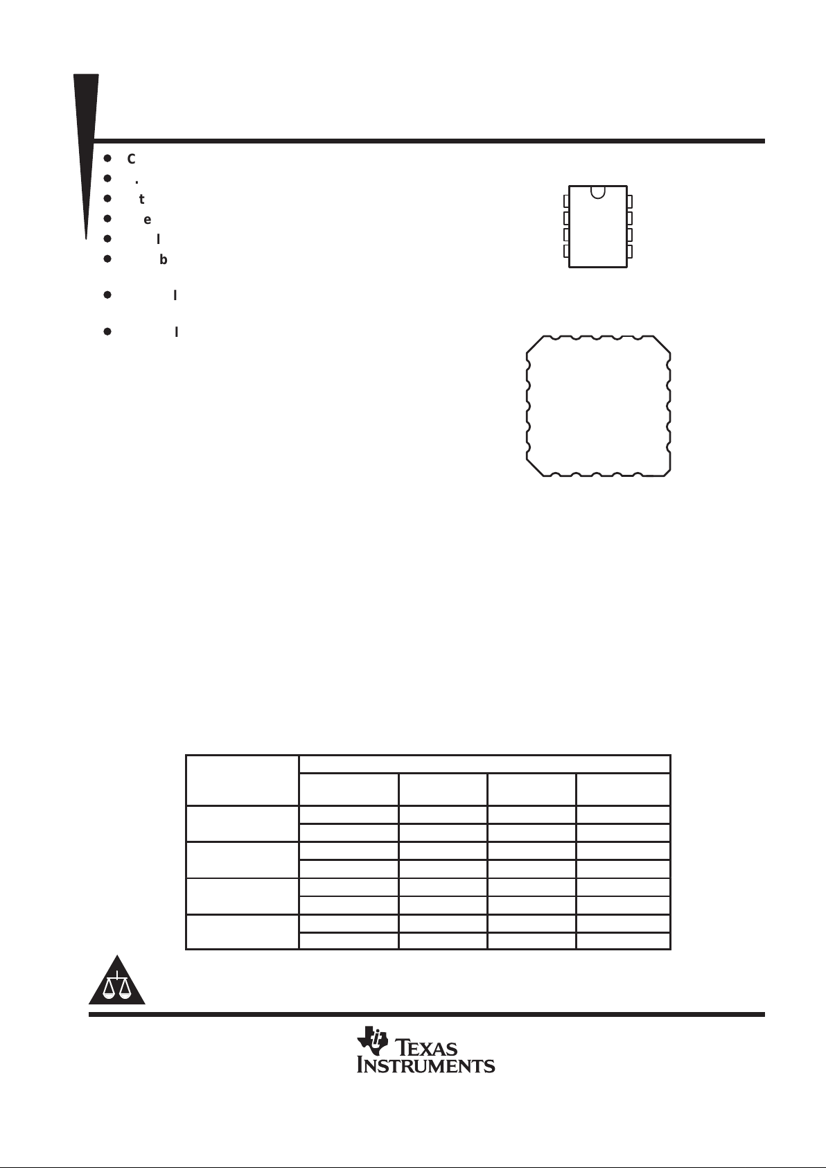
1
2
3
4
8
7
6
5
OUT
V
CC
COMP
FB
GND
RT
DTC
SCP
D, JG OR P PACKAGE
(TOP VIEW)
1920132
17
18
16
15
14
1312119 10
5
4
6
7
8
NC
RT
NC
DTC
NC
NC
V
CC
NC
COMP
NC
NC
OUTNCGND
NC
FB
NC
SCP
NC
NC
FK PACKAGE
(TOP VIEW)
TL5001, TL5001A
PULSE-WIDTH-MODULATION CONTROL CIRCUITS
SLVS084E – APRIL 1994 – REVISED OCT OBER 1999
2
POST OFFICE BOX 655303 • DALLAS, TEXAS 75265
schematic for typical application
TL5001/A
FB
COMP
V
O
DTC
RT
V
I
+
SCP
V
CC
+
TPS1101
GND
8
7
6
5
2
1
3
4
V
O
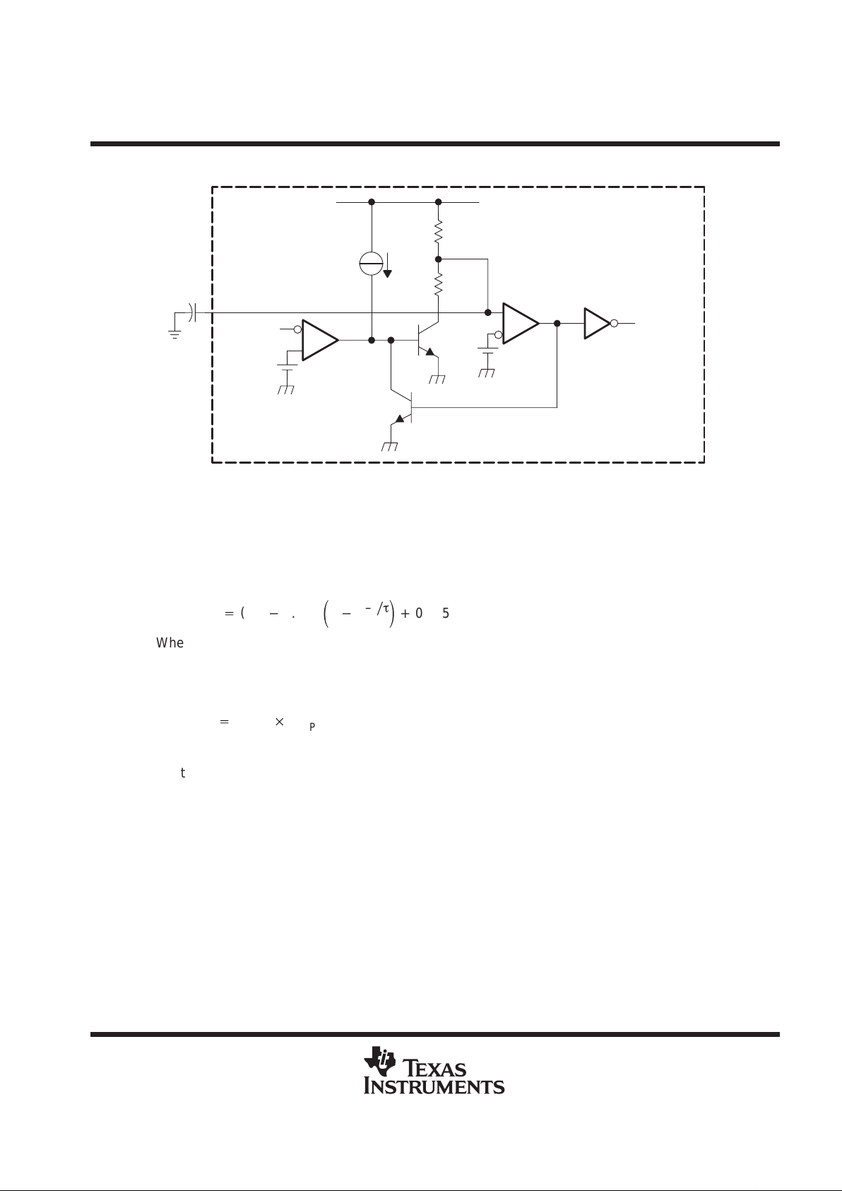
functional block diagram
GND
8
OUT
SCP
COMP
FB
5
3
4
–
+
DTC
RT
67
Comparator 2
SCP
PWM/DTC
Comparator
OSC
Comparator 1
SCP
Amplifier
Error
UVLO
V
CC
2
1
1 V
1.5 V 1 V
Reference
Voltage
I
DT
2.5 V
TL5001, TL5001A
PULSE-WIDTH-MODULATION CONTROL CIRCUITS
SLVS084E – APRIL 1994 – REVISED OCT OBER 1999
3
POST OFFICE BOX 655303 • DALLAS, TEXAS 75265
detailed description
voltage reference
A 2.5-V regulator operating from VCC is used to power the internal circuitry of the TL5001 and TL5001A and
as a reference for the error amplifier and SCP circuits. A resistive divider provides a 1-V reference for the error
amplifier noninverting input which typically is within 2% of nominal over the operating temperature range.
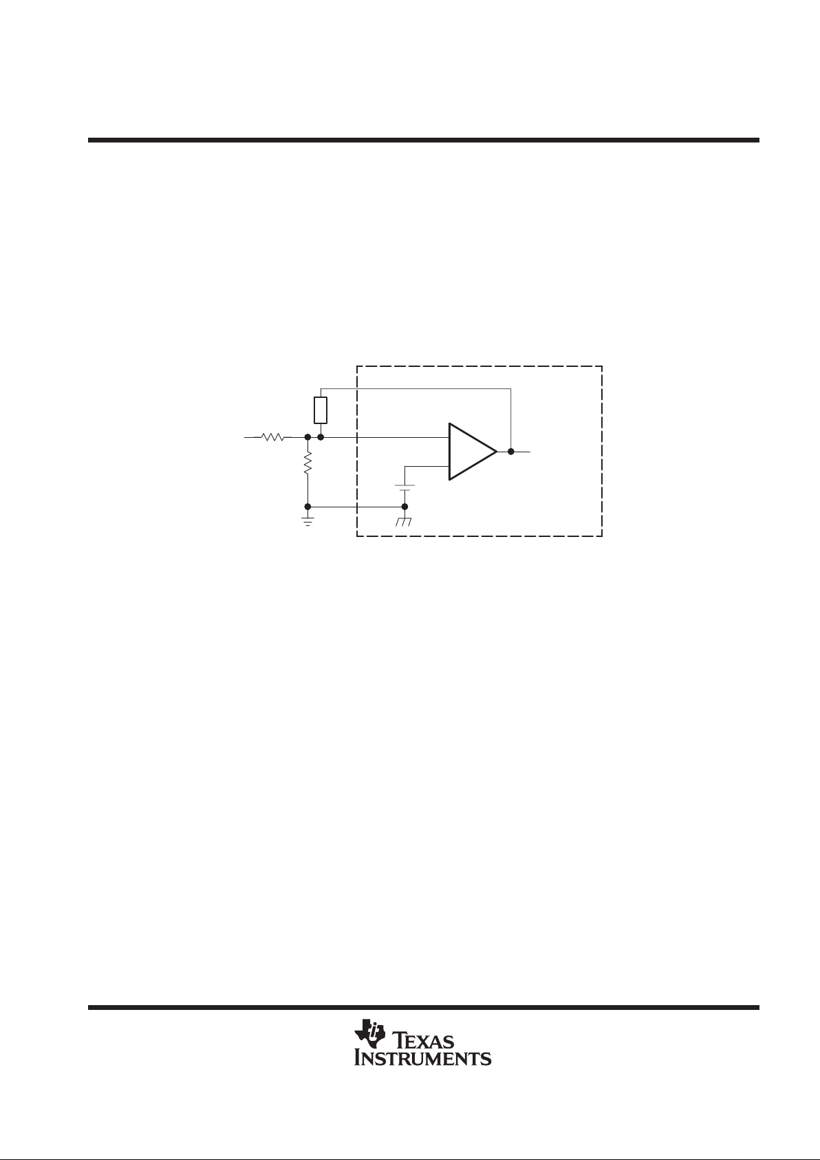
error amplifier
The error amplifier compares a sample of the dc-to-dc converter output voltage to the 1-V reference and
generates an error signal for the PWM comparator. The dc-to-dc converter output voltage is set by selecting
the error-amplifier gain (see Figure 1), using the following expression:
VO = (1 + R1/R2) (1 V)
To PWM
Comparator
V
ref
= 1 V
4
V
I(FB)
3
+
–
R2
R1
COMP
FB
Compensation
Network
TL5001/A
GND
8
Figure 1. Error-Amplifier Gain Setting
The error-amplifier output is brought out as COMP for use in compensating the dc-to-dc converter control loop
for stability . Because the amplifier can only source 45 µA, the total dc load resistance should be 100 kΩ or more.
oscillator/PWM
The oscillator frequency (f
osc
) can be set between 20 kHz and 500 kHz by connecting a resistor between RT
and GND. Acceptable resistor values range from 15 kΩ to 250 kΩ. The oscillator frequency can be determined
by using the graph shown in Figure 5.
The oscillator output is a triangular wave with a minimum value of approximately 0.7 V and a maximum value
of approximately 1.3 V. The PWM comparator compares the error-amplifier output voltage and the DTC input
voltage to the triangular wave and turns the output transistor off whenever the triangular wave is greater than
the lesser of the two inputs.
dead-time control (DTC)
DTC provides a means of limiting the output-switch duty cycle to a value less than 100%, which is critical for
boost and flyback converters. A current source generates a reference current (IDT) at DTC that is nominally
equal to the current at the oscillator timing terminal, RT . Connecting a resistor between DTC and GND generates
a dead-time reference voltage (V
DT
), which the PWM/DTC comparator compares to the oscillator triangle wave
as described in the previous section. Nominally , the maximum duty cycle is 0% when VDT is 0.7 V or less and
100% when VDT is 1.3 V or greater. Because the triangle wave amplitude is a function of frequency and the
source impedance of RT is relatively high (1250 Ω), choosing RDT for a specific maximum duty cycle, D, is
accomplished using the following equation and the voltage limits for the frequency in question as found in
Figure 11 (V
osc
max and V
osc
min are the maximum and minimum oscillator levels):
TL5001, TL5001A
PULSE-WIDTH-MODULATION CONTROL CIRCUITS
SLVS084E – APRIL 1994 – REVISED OCT OBER 1999
4
POST OFFICE BOX 655303 • DALLAS, TEXAS 75265
dead-time control (DTC) (continued)
RDT+ǒRt)
1250
Ǔ
ƪ
DǒV
osc
max – V
osc
minǓ)
V
osc
min
ƫ
Where
RDT and Rt are in ohms, D in decimal
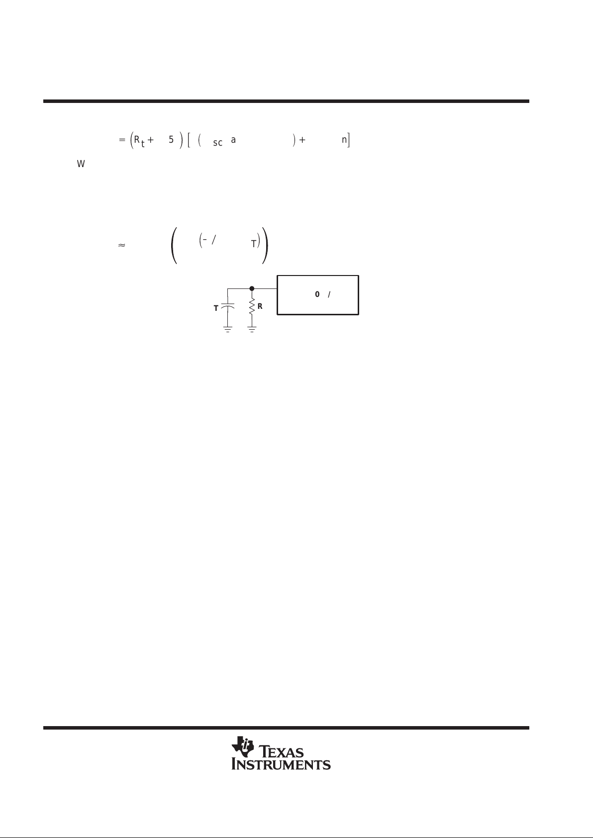
Soft start can be implemented by paralleling the DTC resistor with a capacitor (CDT) as shown in Figure 2. During
soft start, the voltage at DTC is derived by the following equation:
VDT[
IDTR
DT
ǒ
1
–e
ǒ
–tńRDTC
DT
Ǔ
Ǔ
TL5001/A
DTC
C
DT
R
DT
6
Figure 2. Soft-Start Circuit
If the dc-to-dc converter must be in regulation within a specified period of time, the time constant, RDTCDT,
should be t0/3 to t0/5. The TL5001/A remains off until VDT ≈ 0.7 V, the minimum ramp value. CDT is discharged
every time UVLO or SCP becomes active.
undervoltage-lockout (UVLO) protection
The undervoltage-lockout circuit turns the output transistor off and resets the SCP latch whenever the supply
voltage drops too low (approximately 3 V at 25°C) for proper operation. A hysteresis voltage of 200 mV
eliminates false triggering on noise and chattering.
short-circuit protection (SCP)
The TL5001/A includes short-circuit protection (see Figure 3), which turns the power switch off to prevent
damage when the converter output is shorted. When activated, the SCP prevents the switch from being turned
on until the internal latching circuit is reset. The circuit is reset by reducing the input voltage until UVLO becomes
active or until the SCP terminal is pulled to ground externally.
When a short circuit occurs, the error-amplifier output at COMP rises to increase the power-switch duty cycle
in an attempt to maintain the output voltage. SCP comparator 1 starts an RC timing circuit when COMP exceeds
1.5 V . If the short is removed and the error-amplifier output drops below 1.5 V before time out, normal converter
operation continues. If the fault is still present at the end of the time-out period, the timer sets the latching circuit
and turns off the TL5001/A output transistor.
TL5001, TL5001A
PULSE-WIDTH-MODULATION CONTROL CIRCUITS
SLVS084E – APRIL 1994 – REVISED OCT OBER 1999
5
POST OFFICE BOX 655303 • DALLAS, TEXAS 75265
short-circuit protection (SCP) (continued)
Q1
12 kΩ
185 kΩ
R
SCP
Q2
SCP
Comparator 2
V
ref
= 1 V
SCP
Comparator 1
1.5 V
From Error
Amp
C
SCP
To Output
Drive Logic
SCP
5
2.5 V
Figure 3. SCP Circuit
The timer operates by charging an external capacitor (C
SCP
), connected between the SCP terminal and ground,
towards 2.5 V through a 185-kΩ resistor (R
SCP
). The circuit begins charging from an initial voltage of
approximately 185 mV and times out when the capacitor voltage reaches 1 V. The output of SCP comparator
2 then goes high, turns on Q2, and latches the timer circuit. The expression for setting the SCP time period is
derived from the following equation:
V
SCP
+(2.5*0.185
)
ǒ
1*e
–tńt
Ǔ
)
0.185
Where
τ = R
SCPCSCP
The end of the time-out period, t
SCP
, occurs when V
SCP
= 1 V. Solving for C
SCP
yields:
C
SCP
+
12.46 t
SCP
Where
t is in seconds, C in µF.
t
SCP
must be much longer (generally 10 to 15 times) than the converter start-up period or the converter will not
start.
output transistor
The output of the TL5001/A is an open-collector transistor with a maximum collector current rating of 21 mA and
a voltage rating of 51 V. The output is turned on under the following conditions: the oscillator triangle wave is
lower than both the DTC voltage and the error-amplifier output voltage, the UVLO circuit is inactive, and the
short-circuit protection circuit is inactive.
TL5001, TL5001A
PULSE-WIDTH-MODULATION CONTROL CIRCUITS
SLVS084E – APRIL 1994 – REVISED OCT OBER 1999
6
POST OFFICE BOX 655303 • DALLAS, TEXAS 75265
absolute maximum ratings over operating free-air temperature range (unless otherwise noted)
†
Supply voltage, VCC (see Note 1) 41 V. . . . . . . . . . . . . . . . . . . . . . . . . . . . . . . . . . . . . . . . . . . . . . . . . . . . . . . . . . . .
Amplifier input voltage, V
I(FB)
20 V. . . . . . . . . . . . . . . . . . . . . . . . . . . . . . . . . . . . . . . . . . . . . . . . . . . . . . . . . . . . . . .
Output voltage, VO, OUT 51 V. . . . . . . . . . . . . . . . . . . . . . . . . . . . . . . . . . . . . . . . . . . . . . . . . . . . . . . . . . . . . . . . . . .
Output current, I
O
, OUT 21 mA. . . . . . . . . . . . . . . . . . . . . . . . . . . . . . . . . . . . . . . . . . . . . . . . . . . . . . . . . . . . . . . . . .
Output peak current, I
O(peak)
, OUT 100 mA. . . . . . . . . . . . . . . . . . . . . . . . . . . . . . . . . . . . . . . . . . . . . . . . . . . . . . .
Continuous total power dissipation See Dissipation Rating Table. . . . . . . . . . . . . . . . . . . . . . . . . . . . . . . . . . . . .
Operating ambient temperature range, TA: TL5001C, TL5001AC –20°C to 85°C. . . . . . . . . . . . . . . . . . . . . .
TL5001I, TL5001AI –40°C to 85°C. . . . . . . . . . . . . . . . . . . . . . . .
TL5001Q, TL5001AQ –40°C to 125°C. . . . . . . . . . . . . . . . . . . . .
TL5001M, TL5001AM –55°C to 125°C. . . . . . . . . . . . . . . . . . . . .
Storage temperature range, T
stg
–65°C to 150°C. . . . . . . . . . . . . . . . . . . . . . . . . . . . . . . . . . . . . . . . . . . . . . . . . . .
Lead temperature 1,6 mm (1/16 inch) from case for 10 seconds 260°C. . . . . . . . . . . . . . . . . . . . . . . . . . . . . . .
†
Stresses beyond those listed under “absolute maximum ratings” may cause permanent damage to the device. These are stress ratings only, and
functional operation of the device at these or any other conditions beyond those indicated under “recommended operating conditions” is not
implied. Exposure to absolute-maximum-rated conditions for extended periods may affect device reliability.
NOTE 1: All voltage values are with respect to network ground terminal.
DISSIPATION RATING TABLE
PACKAGE
TA ≤ 25°C
POWER RATING
DERATING FACTOR
ABOVE TA = 25°C
TA = 70°C
POWER RATING
TA = 85°C
POWER RATING
TA = 125°C
POWER RATING
D 725 mW 5.8 mW/°C 464 mW 377 mW 145 mW
FK 1375 mW 11.0 mW/°C 880 mW 715 mW 275 mW
JG 1050 mW 8.4 mW/°C 672 mW 546 mW 210 mW
P 1000 mW 8.0 mW/°C 640 mW 520 mW 200 mW
recommended operating conditions
MIN MAX UNIT
Supply voltage, V
CC
3.6 40 V
Amplifier input voltage, V
I(FB)
0 1.5 V
Output voltage, VO, OUT 50 V
Output current, IO, OUT 20 mA
COMP source current 45 µA
COMP dc load resistance 100 kΩ
Oscillator timing resistor, R
t
15 250 kΩ
Oscillator frequency, f
osc
20 500 kHz
TL5001C, TL5001AC –20 85
p
p
TL5001I, TL5001AI –40 85
°
Operating ambient temperature, T
A
TL5001Q, TL5001AQ –40 125
°C
TL5001M, TL5001AM –55 125
TL5001, TL5001A
PULSE-WIDTH-MODULATION CONTROL CIRCUITS
SLVS084E – APRIL 1994 – REVISED OCT OBER 1999
7
POST OFFICE BOX 655303 • DALLAS, TEXAS 75265
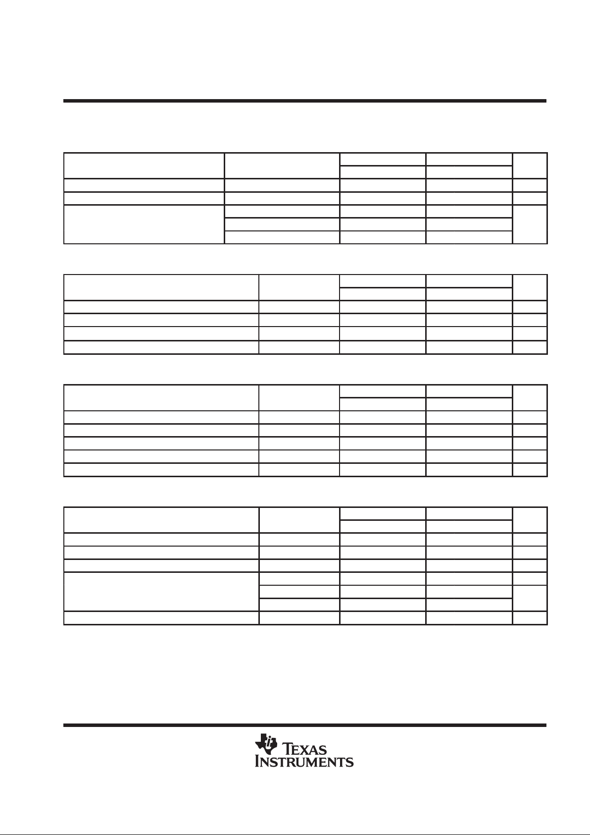
electrical characteristics over recommended operating free-air temperature range, VCC = 6 V,
f
osc
= 100 kHz (unless otherwise noted)
reference
TL5001C, TL5001I TL5001AC, TL5001AI
PARAMETER
TEST CONDITIONS
MIN TYP†MAX MIN TYP†MAX
UNIT
Output voltage COMP connected to FB 0.95 1 1.05 0.97 1 1.03 V
Input regulation VCC = 3.6 V to 40 V 2 12.5 2 12.5 mV
TA = –20°C to 25°C (C suffix) –10 –1 10 –10 –1 10
Output voltage change with temperature
TA = –40°C to 25°C (I suffix) –10 –1 10 –10 –1 10
mV/V
TA = 25°C to 85°C –10 –2 10 –10 –2 10
†
All typical values are at TA = 25°C.
undervoltage lockout
TL5001C, TL5001I TL5001AC, TL5001AI
PARAMETER
TEST CONDITIONS
MIN TYP†MAX MIN TYP†MAX
UNIT
Upper threshold voltage TA = 25°C 3 3 V
Lower threshold voltage TA = 25°C 2.8 2.8 V
Hysteresis TA = 25°C 100 200 100 200 mV
Reset threshold voltage TA = 25°C 2.1 2.55 2.1 2.55 V
†
All typical values are at TA = 25°C.
short-circuit protection
TL5001C, TL5001I TL5001AC, TL5001AI
PARAMETER
TEST CONDITIONS
MIN TYP†MAX MIN TYP†MAX
UNIT
SCP threshold voltage TA = 25°C 0.95 1.00 1.05 0.97 1.00 1.03 V
SCP voltage, latched No pullup 140 185 230 140 185 230 mV
SCP voltage, UVLO standby No pullup 60 120 60 120 mV
Input source current TA = 25°C –10 –15 –20 –10 –15 –20 µA
SCP comparator 1 threshold voltage 1.5 1.5 V
†
All typical values are at TA = 25°C.
oscillator
TL5001C, TL5001I TL5001AC, TL5001AI
PARAMETER
TEST CONDITIONS
MIN TYP†MAX MIN TYP†MAX
UNIT
Frequency Rt = 100 kΩ 100 100 kHz
Standard deviation of frequency 15 15 kHz
Frequency change with voltage VCC = 3.6 V to 40 V 1 1 kHz
TA = –40°C to 25°C –4 –0.4 4 –4 –0.4 4 kHz
Frequency change with temperature
TA = –20°C to 25°C –4 –0.4 4 –4 –0.4 4 kHz
TA = 25°C to 85°C –4 –0.2 4 –4 –0.2 4 kHz
Voltage at RT 1 1 V
†
All typical values are at TA = 25°C.

TL5001, TL5001A
PULSE-WIDTH-MODULATION CONTROL CIRCUITS
SLVS084E – APRIL 1994 – REVISED OCT OBER 1999
8
POST OFFICE BOX 655303 • DALLAS, TEXAS 75265
electrical characteristics over recommended operating free-air temperature range, VCC = 6 V,
f
osc
= 100 kHz (unless otherwise noted) (continued)
dead-time control
TL5001C, TL5001I TL5001AC, TL5001AI
PARAMETER
TEST CONDITIONS
MIN TYP†MAX MIN TYP†MAX
UNIT
p
TL5001C V
(DT)
= 1.5 V 0.9 × I
RT
‡
1.1 × IRT0.9 × I
RT
‡
1.1 × I
RT
Output (source) current
TL5001I V
(DT)
= 1.5 V 0.9 × I
RT
‡
1.2 × IRT0.9 × I
RT
‡
1.2 × I
RT
µ
A
p
Duty cycle = 0% 0.5 0.7 0.5 0.7
Input threshold voltage
Duty cycle = 100% 1.3 1.5 1.3 1.5
V
†
All typical values are at TA = 25°C.
‡
Output source current at RT
error amplifier
TL5001C, TL5001I TL5001AC, TL5001AI
PARAMETER
TEST CONDITIONS
MIN TYP†MAX MIN TYP†MAX
UNIT
Input voltage VCC = 3.6 V to 40 V 0 1.5 0 1.5 V
Input bias current –160 –500 –160 –500 nA
p
Positive 1.5 2.3 1.5 2.3 V
Output voltage swing
Negative 0.3 0.4 0.3 0.4 V
Open-loop voltage amplification 80 80 dB
Unity-gain bandwidth 1.5 1.5 MHz
Output (sink) current V
I(FB)
= 1.2 V , COMP = 1 V 100 600 100 600 µA
Output (source) current V
I(FB)
= 0.8 V , COMP = 1 V –45 –70 –45 –70 µA
†
All typical values are at TA = 25°C.
output
TL5001C, TL5001I TL5001AC, TL5001AI
PARAMETER
TEST CONDITIONS
MIN TYP†MAX MIN TYP†MAX
UNIT
Output saturation voltage IO = 10 mA 1.5 2 1.5 2 V
VO = 50 V, VCC = 0 10 10
Off-state current
VO = 50 V 10 10
µ
A
Short-circuit output current VO = 6 V 40 40 mA
†
All typical values are at TA = 25°C.
total device
TL5001C, TL5001I TL5001AC, TL5001AI
PARAMETER
TEST CONDITIONS
MIN TYP†MAX MIN TYP†MAX
UNIT
Standby supply current Off state 1 1.5 1 1.5 mA
Average supply current Rt = 100 kΩ 1.4 2.1 1.4 2.1 mA
†
All typical values are at TA = 25°C.

TL5001, TL5001A
PULSE-WIDTH-MODULATION CONTROL CIRCUITS
SLVS084E – APRIL 1994 – REVISED OCT OBER 1999
9
POST OFFICE BOX 655303 • DALLAS, TEXAS 75265
electrical characteristics over recommended operating free-air temperature range, VCC = 6 V,
f
osc
= 100 kHz (unless otherwise noted)
reference
PARAMETER TEST CONDITIONS
TL5001Q,
TL5001M
TL5001AQ,
TL5001AM
UNIT
MIN TYP†MAX MIN TYP†MAX
p
TA = MIN, 25°C
0.95 1.00 1.05 0.97 1.00 1.03
Output voltage
TA = MAX
COMP connected to FB
0.93 0.98 1.07 0.94 0.98 1.06
V
Input regulation TA = MIN to MAX VCC = 3.6 V to 40 V 2 12.5 2 12.5 mV
Output voltage change with
temperature
TA = MIN to MAX *–6 2 *6 *–6 2 *6 %
†
All typical values are at TA = 25°C.
*Not production tested.
undervoltage lockout
PARAMETER TEST CONDITIONS
TL5001Q,
TL5001M
TL5001AQ,
TL5001AM
UNIT
PARAMETER
TEST CONDITIONS
MIN TYP†MAX MIN TYP†MAX
UNIT
pp
TA = MIN, 25°C 3.00 3.00
Upper threshold voltage
TA = MAX 2.55 2.55
V
TA = MIN, 25°C 2.8 2.8
Lower threshold voltage
TA = MAX 2.0 2.0
V
Hysteresis TA = MIN to MAX 100 200 100 200 mV
TA = MIN, 25°C 2.10 2.55 2.10 2.55
Reset threshold voltage
TA = MAX 0.35 0.63 0.35 0.63
V
†
All typical values are at TA = 25°C.
short-circuit protection
PARAMETER TEST CONDITIONS
TL5001Q,
TL5001M
TL5001AQ,
TL5001AM
UNIT
MIN TYP†MAX MIN TYP†MAX
TA = MIN, 25°C 0.95 1.00 1.05 0.97 1.00 1.03
SCP threshold voltage
TA = MAX 0.93 0.98 1.07 0.94 0.98 1.06
V
SCP voltage, latched TA = MIN to MAX No pullup 140 185 230 140 185 230 mV
SCP voltage, UVLO standby TA = MIN to MAX No pullup 60 120 60 120 mV
Equivalent timing resistance TA = MIN to MAX 185 185 kΩ
SCP comparator 1 threshold voltage TA = MIN to MAX 1.5 1.5 V
†
All typical values are at TA = 25°C.

TL5001, TL5001A
PULSE-WIDTH-MODULATION CONTROL CIRCUITS
SLVS084E – APRIL 1994 – REVISED OCT OBER 1999
10
POST OFFICE BOX 655303 • DALLAS, TEXAS 75265
electrical characteristics over recommended operating free-air temperature range, VCC = 6 V,
f
osc
= 100 kHz (unless otherwise noted) (continued)
oscillator
PARAMETER TEST CONDITIONS
TL5001Q,
TL5001M
TL5001AQ,
TL5001AM
UNIT
MIN TYP†MAX MIN TYP†MAX
Frequency TA = MIN to MAX Rt = 100 kΩ 100 100 kHz
Standard deviation of frequency TA = MIN to MAX 2 2 kHz
Frequency change with voltage TA = MIN to MAX VCC = 3.6 V to 40 V 1 1 kHz
Frequency change with
Q suffix *–6 3 *6 *–6 3 *6
Frequency change with
temperature
T
A
=
MIN to MAX
M suffix *–9 5 *9 *–9 5 *9
kH
z
Voltage at RT TA = MIN to MAX 1 1 V
†
All typical values are at TA = 25°C.
*Not production tested.
dead-time control
TL5001Q, TL5001M TL5001AQ, TL5001AM
PARAMETER
TEST CONDITIONS
MIN TYP†MAX MIN TYP†MAX
UNIT
Output (source)
current
TA = MIN to MAX V
(DT)
= 1.5 V 0.9 × I
RT
‡
1.1 × IRT0.9 × I
RT
‡
1.1 × I
RT
µA
°
Duty cycle = 0% 0.5 0.7 0.5 0.7
Input threshold
T
A
=
25°C
Duty cycle = 100% 1.3 1.5 1.3 1.5
voltage
Duty cycle = 0% 0.4 0.7 0.4 0.7
V
T
A
=
MIN to MAX
Duty cycle = 100% 1.3 1.7 1.3 1.7
†
All typical values are at TA = 25°C.
‡
Output source current at RT
error amplifier
PARAMETER TEST CONDITIONS
TL5001Q,
TL5001M
TL5001AQ,
TL5001AM
UNIT
PARAMETER
TEST CONDITIONS
MIN TYP†MAX MIN TYP†MAX
UNIT
Input bias current TA = MIN to MAX –160 –500 –160 –500 nA
Output voltage
Positive
1.5 2.3 1.5 2.3 V
Out ut voltage
swing
Negative
T
A
=
MIN to MAX
0.3 0.4 0.3 0.4 V
Open-loop voltage
amplification
TA = MIN to MAX 80 80 dB
Unity-gain bandwidth TA = MIN to MAX 1.5 1.5 MHz
Output (sink) current TA = MIN to MAX V
I(FB)
= 1.2 V , COMP = 1 V 100 600 100 600 µA
p
TA = MIN, 25°C
–45 –70 –45 –70
Output (source) current
TA = MAX
V
I(FB)
= 0.8 V,
COMP
= 1
V
–30 –45 –30 –45
µ
A
†
All typical values are at TA = 25°C.

TL5001, TL5001A
PULSE-WIDTH-MODULATION CONTROL CIRCUITS
SLVS084E – APRIL 1994 – REVISED OCT OBER 1999
11
POST OFFICE BOX 655303 • DALLAS, TEXAS 75265
electrical characteristics over recommended operating free-air temperature range, VCC = 6 V,
f
osc
= 100 kHz (unless otherwise noted) (continued)
output
PARAMETER TEST CONDITIONS
TL5001Q,
TL5001M
TL5001AQ,
TL5001AM
UNIT
MIN TYP†MAX MIN TYP†MAX
Output saturation voltage TA = MIN to MAX IO = 10 mA 1.5 2 1.5 2 V
VO = 50 V, VCC = 0 10 10
Off-state current
T
A
=
MIN to MAX
VO = 50 V 10 10
µ
A
Short-circuit output current TA = MIN to MAX VO = 6 V 40 40 mA
†
All typical values are at TA = 25°C.
total device
PARAMETER TEST CONDITIONS
TL5001Q,
TL5001M
TL5001AQ,
TL5001AM
UNIT
PARAMETER
TEST CONDITIONS
MIN TYP†MAX MIN TYP†MAX
UNIT
Standby supply current Off state TA = MIN to MAX 1 1.5 1 1.5 mA
Average supply current TA = MIN to MAX Rt = 100 kΩ 1.4 2.1 1.4 2.1 mA
†
All typical values are at TA = 25°C.

TL5001, TL5001A
PULSE-WIDTH-MODULATION CONTROL CIRCUITS
SLVS084E – APRIL 1994 – REVISED OCT OBER 1999
12
POST OFFICE BOX 655303 • DALLAS, TEXAS 75265
PARAMETER MEASUREMENT INFORMATION
2.3 V
SCP Timing Period
3 V
DTC
OSC
COMP
1 V
0 V
PWM/DTC
Comparator
OUT
SCP
Comparator 1
SCP
SCP
Comparator 2
V
CC
1.5 V
NOTE A: The waveforms show timing characteristics for an intermittent short circuit and a longer short circuit that is sufficient to activate SCP.
Figure 4. PWM Timing Diagram

TL5001, TL5001A
PULSE-WIDTH-MODULATION CONTROL CIRCUITS
SLVS084E – APRIL 1994 – REVISED OCT OBER 1999
13
POST OFFICE BOX 655303 • DALLAS, TEXAS 75265
TYPICAL CHARACTERISTICS
Figure 5
100 k
10 k
1 M
10 k 100 k 1 M
f
VCC = 6 V
DT Resistance = R
t
TA = 25°C
Rt – Timing Resistance – Ω
OSCILLATOR FREQUENCY
vs
TIMING RESISTANCE
– Oscillator Frequency – Hz
osc
Figure 6
94
92
90
88
– 50 – 25 0
96
98
100
25 50 75 100
TA – Ambient Temperature – °C
OSCILLATION FREQUENCY
vs
AMBIENT TEMPERATURE
f – Oscillation Frequency – kHz
osc
VCC = 6 V
Rt = 100 kΩ
DT Resistance = 100 kΩ
Figure 7
REFERENCE OUTPUT VOLTAGE
vs
POWER-SUPPLY VOLTAGE
– Reference Output Voltage – VV
ref
VCC – Power-Supply Voltage – V
1
0.8
0.4
0.2
0
1.8
0.6
0123456
1.4
1.2
1.6
2
78910
TA = 25°C
FB and COMP
Connected Together
Figure 8
– Reference Output Voltage Fluctuation – %
TA – Ambient Temperature – °C
∆V
ref
REFERENCE OUTPUT VOLTAGE FLUCTUATION
vs
AMBIENT TEMPERATURE
– 0.2
– 0.4
– 0.8
– 50 – 25 0
0.2
0.4
0.6
25 50 75 100
0
VCC = 6 V
FB and COMP
Connected Together
– 0.6

TL5001, TL5001A
PULSE-WIDTH-MODULATION CONTROL CIRCUITS
SLVS084E – APRIL 1994 – REVISED OCT OBER 1999
14
POST OFFICE BOX 655303 • DALLAS, TEXAS 75265
TYPICAL CHARACTERISTICS
Figure 9
1
0.5
0
2
1.5
010203040
– Average Supply Current – mA
VCC – Power-Supply Voltage – V
Rt = 100 kΩ
TA = 25 °C
AVERAGE SUPPLY CURRENT
vs
POWER-SUPPLY VOLTAGE
I
CC
Figure 10
1
0.9
0.8
0
– 50 – 25 0
– Average Supply Current – mA
1.1
1.2
1.3
25 50 75 100
TA – Ambient Temperature – °C
VCC = 6 V
Rt = 100 kΩ
DT Resistance = 100 kΩ
I
CC
AVERAGE SUPPLY CURRENT
vs
AMBIENT TEMPERATURE
Figure 11
1.5
1.2
0.6
0.3
0
1.8
0.9
10 k 100 k 1 M 10 M
PWM Triangle Wave Amplitude Voltage – V
f
osc
– Oscillator Frequency – Hz
V
osc
min (zero duty cycle)
VCC = 6 V
TA = 25 °C
PWM TRIANGLE WAVE AMPLITUDE VOLTAGE
vs
OSCILLATOR FREQUENCY
V
osc
max (100% duty cycle)
Figure 12
ERROR AMPLIFIER OUTPUT VOLTAGE
vs
OUTPUT (SINK) CURRENT
– Error Amplifier Output V oltage – V
V
O
IO – Output (Sink) Current – mA
1.5
1
0.5
0
0 0.2 0.4
2
2.5
3
0.6
VCC = 6 V
V
I(FB)
= 1.2 V
TA = 25
°C

TL5001, TL5001A
PULSE-WIDTH-MODULATION CONTROL CIRCUITS
SLVS084E – APRIL 1994 – REVISED OCT OBER 1999
15
POST OFFICE BOX 655303 • DALLAS, TEXAS 75265
TYPICAL CHARACTERISTICS
Figure 13
1.5
1
0.5
0
02040
– Error Amplifier Output V oltage – V
2
2.5
3
60 80 100 120
V
O
IO – Output (Source) Current – µA
VCC = 6 V
V
I(FB)
= 0.8 V
TA = 25 °C
ERROR AMPLIFIER OUTPUT VOLTAGE
vs
OUTPUT (SOURCE) CURRENT
Figure 14
2.43
2.42
2.41
2.40
– 50 – 25 0
– Error Amplifier Output V oltage – V
2.44
2.45
2.46
25 50 75
100
V
O
TA – Ambient Temperature – °C
VCC = 6 V
V
I(FB)
= 0.8 V
No Load
ERROR AMPLIFIER OUTPUT VOLTAGE
vs
AMBIENT TEMPERATURE
Figure 15
180
160
140
120
– 50 – 25 0
– Error Amplifier Output V oltage – mV
200
220
240
25 50 75
100
V
O
TA – Ambient Temperature – °C
VCC = 6 V
V
I(FB)
= 1.2 V
No Load
ERROR AMPLIFIER OUTPUT VOLTAGE
vs
AMBIENT TEMPERATURE
Figure 16
30
20
0
– 10
– 20
40
10
10 k 100 k 1 M 10 M
– Error Amplifier Closed-Loop Gain – dB
f
osc
– Oscillator Frequency – Hz
VCC = 6 V
TA = 25 °C
A
V
φ
A
V
ERROR AMPLIFIER CLOSED-LOOP GAIN AND
PHASE SHIFT
vs
OSCILLATOR FREQUENCY
–180
°
–210
°
–240
°
–270
°
–300
°
–330
°
–360
°

TL5001, TL5001A
PULSE-WIDTH-MODULATION CONTROL CIRCUITS
SLVS084E – APRIL 1994 – REVISED OCT OBER 1999
16
POST OFFICE BOX 655303 • DALLAS, TEXAS 75265
TYPICAL CHARACTERISTICS
Figure 17
60
40
20
0
0 0.5 1
80
100
120
1.5 2
DTC Voltage – V
OUTPUT DUTY CYCLE
vs
DTC VOLTAGE
Output Duty Cycle – %
VCC = 6 V
Rt = 100 kΩ
TA = 25 °C
Figure 18
6
4
2
0
02040
– SCP Time-Out Period – ms
8
10
12
60 80 100 120
VCC = 6 V
Rt = 100 kΩ
DT Resistance = 200 kΩ
TA = 25 °C
C
SCP
– SCP Capacitance – nF
t
SCP
SCP TIME-OUT PERIOD
vs
SCP CAPACITANCE
Figure 19
– 30
– 20
– 10
0
0 – 10 – 20
– DTC Output Current –
– 40
– 50
– 60
– 30 – 40 – 50 – 60
DT Voltage = 1.3 V
TA = 25 °C
IO – RT Output Current – µA
AµI
O(DT)
DTC OUTPUT CURRENT
vs
RT OUTPUT CURRENT
Figure 20
1
0.5
0
2
1.5
0 5 10 15 20
– Output Saturation Voltage – V
IO – Output (Sink) Current – mA
V
CE
VCC = 6 V
TA = 25 °C
OUTPUT SATURATION VOLTAGE
vs
OUTPUT (SINK) CURRENT

TL5001, TL5001A
PULSE-WIDTH-MODULATION CONTROL CIRCUITS
SLVS084E – APRIL 1994 – REVISED OCT OBER 1999
17
POST OFFICE BOX 655303 • DALLAS, TEXAS 75265
APPLICATION INFORMATION
U1
TL5001/A
FB
COMP
V
O
DTC
RT
GND
C1
100 µF
10 V
V
I
5 V
+
R1
470 Ω
SCP
V
CC
L1
20 µH
C2
100 µF
10 V
3.3 V
GND
+
CR1
MBRS140T3
Q1
TPS1101
C6
0.012 µF
R4
5.1 kΩ
R5
7.50 kΩ
1%
R2
56 kΩ
R3
43 kΩ
R6
3.24 kΩ
1%
C5
0.1 µF
C4
1 µF
C3
0.1 µF
GND
8
7
6
5
2
1
3
4
Partial Bill of Materials:
U1 TL5001/A Texas Instruments
Q1 TPS1101 Texas Instruments
LI CTX20-1 or Coiltronics
23 turns of #28 wire on
Micrometals No. T50-26B core
C1 TPSD107M010R0100 AVX
C2 TPSD107M010R0100 AVX
CR1 MBRS140T3 Motorola
R7
2.0 kΩ
C7
0.0047 µF
+
NOTES: A. Frequency = 200 kHz
B. Duty cycle = 90% max
C. Soft-start time constant (TC) = 5.6 ms
D. SCP TC = 70 msA
Figure 21. Step-Down Converter

TL5001, TL5001A
PULSE-WIDTH-MODULATION CONTROL CIRCUITS
SLVS084E – APRIL 1994 – REVISED OCT OBER 1999
18
POST OFFICE BOX 655303 • DALLAS, TEXAS 75265
MECHANICAL DATA
D (R-PDSO-G**) PLASTIC SMALL-OUTLINE PACKAGE
14 PIN SHOWN
4040047/D 10/96
0.228 (5,80)
0.244 (6,20)
0.069 (1,75) MAX
0.010 (0,25)
0.004 (0,10)
1
14
0.014 (0,35)
0.020 (0,51)
A
0.157 (4,00)
0.150 (3,81)
7
8
0.044 (1,12)
0.016 (0,40)
Seating Plane
0.010 (0,25)
PINS **
0.008 (0,20) NOM
A MIN
A MAX
DIM
Gage Plane
0.189
(4,80)
(5,00)
0.197
8
(8,55)
(8,75)
0.337
14
0.344
(9,80)
16
0.394
(10,00)
0.386
0.004 (0,10)
M
0.010 (0,25)
0.050 (1,27)
0°–8°
NOTES: B. All linear dimensions are in inches (millimeters).
C. This drawing is subject to change without notice.
D. Body dimensions do not include mold flash or protrusion, not to exceed 0.006 (0,15).
E. Falls within JEDEC MS-012

TL5001, TL5001A
PULSE-WIDTH-MODULATION CONTROL CIRCUITS
SLVS084E – APRIL 1994 – REVISED OCT OBER 1999
19
POST OFFICE BOX 655303 • DALLAS, TEXAS 75265
MECHANICAL DATA
FK (S-CQCC-N**) LEADLESS CERAMIC CHIP CARRIER
4040140/C 11/95
28 TERMINALS SHOWN
B
0.358
(9,09)
MAX
(11,63)
0.560
(14,22)
0.560
0.458
0.858
(21,8)
1.063
(27,0)
(14,22)
A
NO. OF
MINMAX
0.358
0.660
0.761
0.458
0.342
(8,69)
MIN
(11,23)
(16,26)
0.640
0.740
0.442
(9,09)
(11,63)
(16,76)
0.962
1.165
(23,83)
0.938
(28,99)
1.141
(24,43)
(29,59)
(19,32)(18,78)
**
20
28
52
44
68
84
0.020 (0,51)
TERMINALS
0.080 (2,03)
0.064 (1,63)
(7,80)
0.307
(10,31)
0.406
(12,58)
0.495
(12,58)
0.495
(21,6)
0.850
(26,6)
1.047
0.045 (1,14)
0.045 (1,14)
0.035 (0,89)
0.035 (0,89)
0.010 (0,25)
12
1314151618 17
11
10
8
9
7
5
432
0.020 (0,51)
0.010 (0,25)
6
12826 27
19
21
B SQ
A SQ
22
23
24
25
20
0.055 (1,40)
0.045 (1,14)
0.028 (0,71)
0.022 (0,54)
0.050 (1,27)
NOTES: A. All linear dimensions are in inches (millimeters).
B. This drawing is subject to change without notice.
C. This package can be hermetically sealed with a metal lid.
D. The terminals are gold-plated.
E. Falls within JEDEC MS-004

MECHANICAL DATA
MCER001A – JANUARY 1995 – REVISED JANUARY 1997
20
POST OFFICE BOX 655303 • DALLAS, TEXAS 75265
MECHANICAL DATA
JG (R-GDIP-T8) CERAMIC DUAL-IN-LINE
0.310 (7,87)
0.290 (7,37)
0.014 (0,36)
0.008 (0,20)
Seating Plane
4040107/C 08/96
5
4
0.065 (1,65)
0.045 (1,14)
8
1
0.020 (0,51) MIN
0.400 (10,16)
0.355 (9,00)
0.015 (0,38)
0.023 (0,58)
0.063 (1,60)
0.015 (0,38)
0.200 (5,08) MAX
0.130 (3,30) MIN
0.245 (6,22)
0.280 (7,11)
0.100 (2,54)
0°–15°
NOTES: A. All linear dimensions are in inches (millimeters).
B. This drawing is subject to change without notice.
C. This package can be hermetically sealed with a ceramic lid using glass frit.
D. Index point is provided on cap for terminal identification.
E. Falls within MIL STD 1835 GDIP1-T8

MECHANICAL DATA
MCER001A – JANUARY 1995 – REVISED JANUARY 1997
21
POST OFFICE BOX 655303 • DALLAS, TEXAS 75265
MECHANICAL INFORMATION
P (R-PDIP-T8) PLASTIC DUAL-IN-LINE PACKAGE
4040082/B 03/95
0.310 (7,87)
0.290 (7,37)
0.010 (0,25) NOM
0.400 (10,60)
0.355 (9,02)
58
41
0.020 (0,51) MIN
0.070 (1,78) MAX
0.240 (6,10)
0.260 (6,60)
0.200 (5,08) MAX
0.125 (3,18) MIN
0.015 (0,38)
0.021 (0,53)
Seating Plane
M
0.010 (0,25)
0.100 (2,54)
0°–15°
NOTES: A. All linear dimensions are in inches (millimeters).
B. This drawing is subject to change without notice.
C. Falls within JEDEC MS-001

MECHANICAL DATA
MCER001A – JANUARY 1995 – REVISED JANUARY 1997
22
POST OFFICE BOX 655303 • DALLAS, TEXAS 75265

IMPORTANT NOTICE
T exas Instruments and its subsidiaries (TI) reserve the right to make changes to their products or to discontinue
any product or service without notice, and advise customers to obtain the latest version of relevant information
to verify, before placing orders, that information being relied on is current and complete. All products are sold
subject to the terms and conditions of sale supplied at the time of order acknowledgement, including those
pertaining to warranty, patent infringement, and limitation of liability.
TI warrants performance of its semiconductor products to the specifications applicable at the time of sale in
accordance with TI’s standard warranty. Testing and other quality control techniques are utilized to the extent
TI deems necessary to support this warranty. Specific testing of all parameters of each device is not necessarily
performed, except those mandated by government requirements.
CERT AIN APPLICATIONS USING SEMICONDUCTOR PRODUCTS MAY INVOLVE POTENTIAL RISKS OF
DEATH, PERSONAL INJURY, OR SEVERE PROPERTY OR ENVIRONMENTAL DAMAGE (“CRITICAL
APPLICATIONS”). TI SEMICONDUCTOR PRODUCTS ARE NOT DESIGNED, AUTHORIZED, OR
WARRANTED TO BE SUITABLE FOR USE IN LIFE-SUPPORT DEVICES OR SYSTEMS OR OTHER
CRITICAL APPLICATIONS. INCLUSION OF TI PRODUCTS IN SUCH APPLICA TIONS IS UNDERSTOOD T O
BE FULLY AT THE CUSTOMER’S RISK.
In order to minimize risks associated with the customer’s applications, adequate design and operating
safeguards must be provided by the customer to minimize inherent or procedural hazards.
TI assumes no liability for applications assistance or customer product design. TI does not warrant or represent
that any license, either express or implied, is granted under any patent right, copyright, mask work right, or other
intellectual property right of TI covering or relating to any combination, machine, or process in which such
semiconductor products or services might be or are used. TI’s publication of information regarding any third
party’s products or services does not constitute TI’s approval, warranty or endorsement thereof.
Copyright 1999, Texas Instruments Incorporated
 Loading...