

Page 1
•
Programmable Output Voltage to 36V
•
Low Dynamic Output Impedance 0.2Ω
•
Sink Current Capability of 0.1 mA to 100 mA
•
Equivalent Full-Range Temperature Coefficient of 50 ppm/
o
C
•
Temperature Compensated for Operation over Full Rated
Operating Temperature Range
•
Low Output Noise Voltage
•
Fast Turn on Response
DESCRIPTION
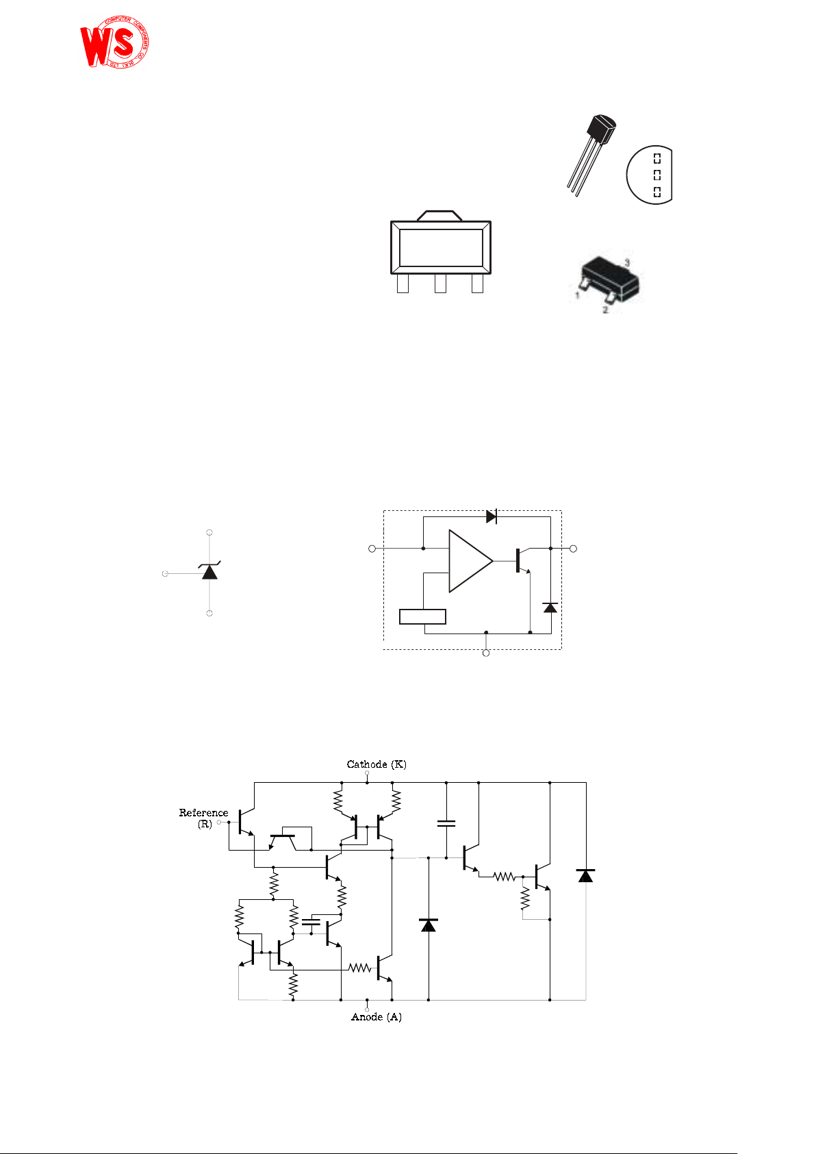
The TL431 is a three-terminal adjustable regulator series with a guaranteed thermal stability over
applicable temperature ranges. The output voltage may be set to any value between Vref
(approximately 2.5 volts) and 36 volts with two external resistors. These devices have a typical
dynamic output impedance of 0.2Ω. Active output circuitry provides a very sharp turn-on
characteristic, making these devices excellent replacement for zener diodes in many applications.
The TL431 is characterized for operation from 0oC to +70oC.
SYMBOL FUNCTIONAL BLOCK DIAGRAM
SCHEMATIC DIAGRAM
Re ference
(R )
Cathod e
(K )
Anode (A)
2.5V
ref
+
-
Re ference
(R )
Cathod e
(K )
Anode
(A )
Wing Shing Computer Components Co., (H.K.)Ltd. Tel:(852)2341 9276 Fax:(852)2797 8153
Homepage: http://www.wingshing.com E-mail: [email protected]
SOT————23
Page 2

ABSOLUTE MAXIMUM RATINGS
(Operating temperature range applies unless otherwise specified)
Characteristic Symbol Value Unit
Cathode Voltage VKA 37 V
Cathode Current Range (Continuous) IK -100 ~ +150 mA
Reference Input Current Range I
REF
0.05 ~ +10 mA
Operating Temperature Range Ta 0 ~ +70
o
C
Storage Temperature Range T
stg
-65 ~ +150
o
C
RECOMMENDED OPERATING CONDITIONS
Characteristic Symbol Test Condition Min Typ Max Unit
Cathode Voltage VKA V
REF
36 V
Cathode Current IK 1.0 100 mA
ELECTRICAL CHARACTERISTICS
(Ta = 25oC, unless otherwise specified)
Characteristic Symbol Test Condition Min Typ Max Unit
Reference Input Voltage V
REF
V
KA = VREF
, IK = 10mA 2.44 2.495 2.55 V
Deviation of Reference
Input Voltage OverTemperature (Note 1)
V
REF(dev)
VKA = V
REF
, IK = 10mA
T
min
≤ Ta ≤ T
max
4 17 mV
Ratio of Change in
Reference Input Voltage
to the Change in
∆
∆VV
REF
KA
I
K
= 10mA
∆
V
KA
= 10V-V
REF
-1.4 -2.7
mV/V
Cathode Voltage
∆
K
KA
= 36V-10V
-1.0 -2.0
Reference Input Current I
REF
I
K
= 10mA, R1 = 10KΩ, R2 = ∞
2,0 4
µ
A
Deviation of Reference
Input Current Over Full
Temperature Range
I
REF(dev)
IK = 10mA, R1 = 10KΩ, R2 = ∞
Ta = Full Range
0.4 1.2
µ
A
Minimum Cathode
Current for Regulation
I
K(min)
V
KA = VREF
0.4 1.0 mA
Off-State Cathode
Current
I
K(off)
V
KA =
36V, V
REF
= 0 0.1 1.0
µ
A
Dynamic Impedance
(Note2)
ZKA V
KA = VREF
, IK = 10mA to
100mA
f ≤ 1.0KHz
0.2 0.5
Ω
Page 3
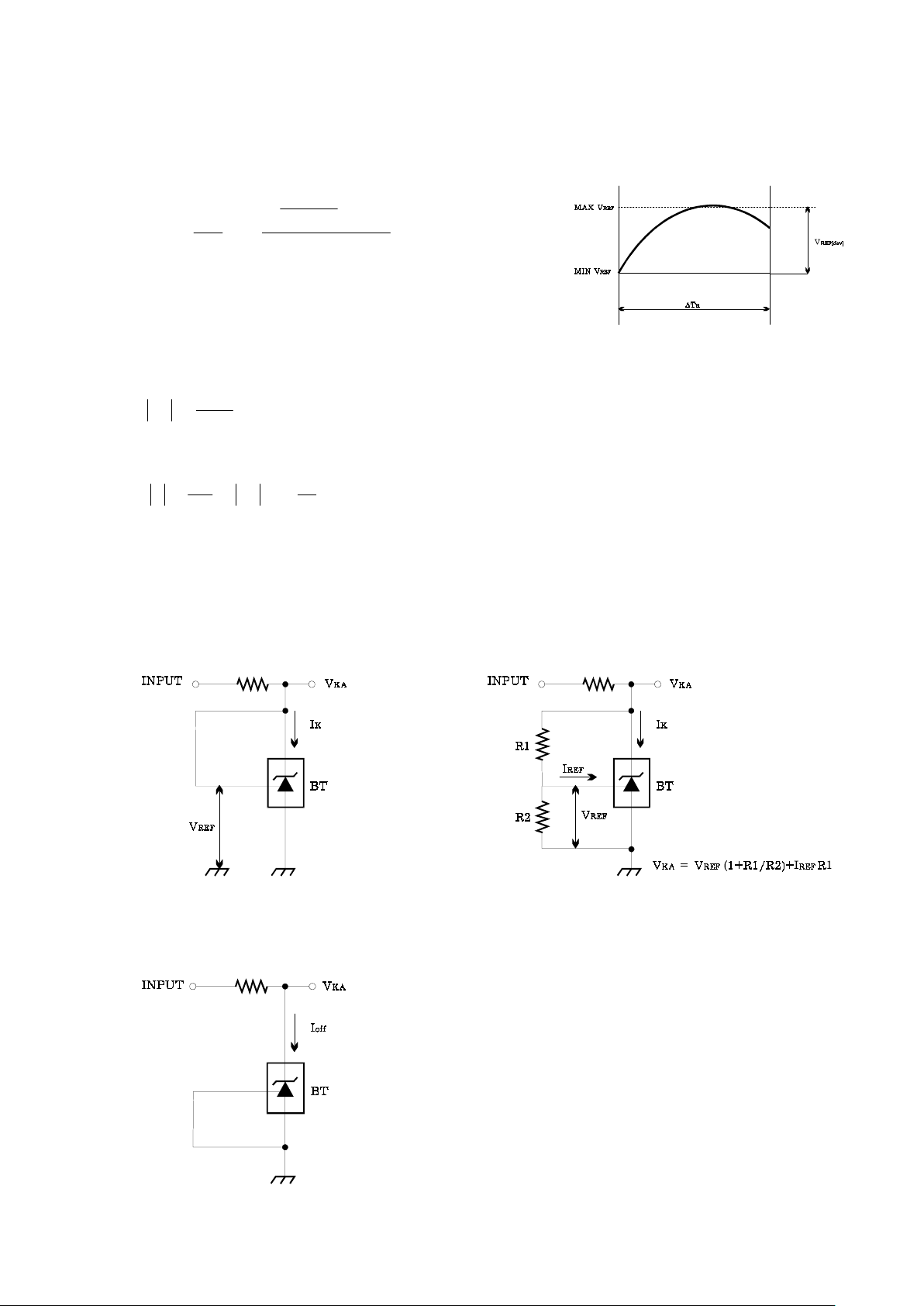
Note: 1. The deviation parameters V
REF(dev)
and I
REF(dev)
are defined as the differences between the maximum and minimum
values obtained over the rated temperature range.
V
REF(dev)
= V
REF
(max) - V
REF
(min)
The equivalent full-range temperature coefficient of the reference input voltage, αV
REF
is defined as:
αV
REF
(
)
ppm
C
°
=
( )
V
V@C
Ta
REF(dev)
REF
°
×
10
6
∆
where ∆Ta is the rated operating free-air temperature range of the device.
αV
REF
can be positive or negative depending on whether minimum
V
REF
or ma ximum V
REF
respectively, occurs at the lower temperature.
2. The dynamic impedance is defined as:
Z
KA
=
∆
∆
V
I
KA
K
When the device is operated with two external resistors (see Figure 2), the total dynamic impedance of the circuit is
given by:
Z
'
=
∆
∆
V
I
=
Z
KA
(1+
R
R
1
2
)
TEST CIRCUITS
Fig.1. Test Circuit for VKA = V
REF
Fig.2. Test Circuit for VKA
≥≥≥≥
V
REF
Fig.3. Test Circuit for I
off
Page 4
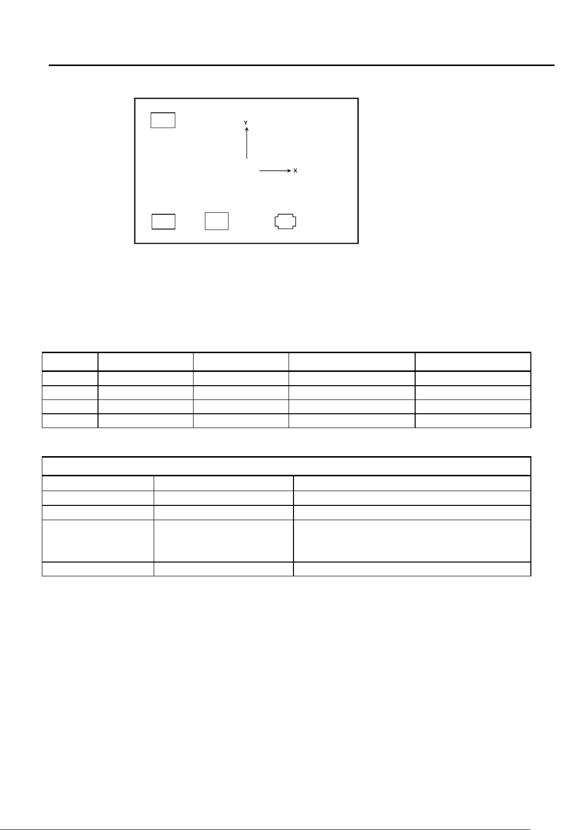
PAD LAYOUT
PAD LOCATION
Unit: µm
Pad No. Pad Name Desc ription X Y
1 R Reference 235 400
2 K Cathode -505 343.5
3 K Cathode -497.5 -346
4 A Anode -177.5 -341.5
Physical Characteristics
Wafers 4 inch
460 ± 40 µm (thickness)
Size
1.35 × 0.99 mm
Scribe width
90 µm
Wafer’s Backside
Ti – Ni – Ag: Ti - 0.1 ± 0.02 µm
Ni - 0.5 ± 0.1 µm
Ag - 0.6 ± 0.1 µm
Passivation PSG
TL431 PAD DI AGRAM
Chi p size: 1345 x 990
P ad size :
Unit : m
µ
(0 ,0 )
2
34
1
 Loading...