

Page 1
V
ref
Input
V
KA
I
KA
SLVS543Q – AUGUST 2004 – REVISED JULY 2022
TL431, TL432 Precision Programmable Reference
TL431, TL432
1 Features
• Reference voltage tolerance at 25°C
– 0.5% (B grade)
– 1% (A grade)
– 2% (Standard grade)
• Adjustable output voltage: V
to 36 V
ref
• Operation from −40°C to 125°C
• Typical temperature drift (TL43xB)
– 6 mV (C temp)
– 14 mV (I temp, Q temp)
• Low Output Noise
• 0.2-Ω Typical output impedance
• Sink-current capability: 1 mA to 100 mA
2 Applications
• Adjustable voltage and current referencing
• Secondary side regulation in flyback SMPSs
• Zener replacement
• Voltage monitoring
• Comparator with integrated reference
3 Description
The TL431LI / TL432LI are pin-to-pin alternatives
to TL431 / TL432. TL43xLI offers better stability,
lower temperature drift (V
reference current (I
) for improved system
ref
accuracy.
The TL431 and TL432 devices are three-terminal
adjustable shunt regulators, with specified thermal
stability over applicable automotive, commercial, and
military temperature ranges. The output voltage can
be set to any value between V
ref
2.5 V) and 36 V, with two external resistors.
These devices have a typical output impedance
of 0.2 Ω. Active output circuitry provides a very
sharp turn-on characteristic, making these devices
excellent replacements for Zener diodes in many
applications, such as onboard regulation, adjustable
power supplies, and switching power supplies. The
TL432 device has exactly the same functionality and
electrical specifications as the TL431 device, but has
different pinouts for the DBV, DBZ, and PK packages.
Both the TL431 and TL432 devices are offered in
three grades, with initial tolerances (at 25°C) of
0.5%, 1%, and 2%, for the B, A, and standard
grade, respectively. In addition, low output drift versus
temperature ensures good stability over the entire
temperature range.
), and lower
I(dev)
(approximately
The TL43xxC devices are characterized for operation
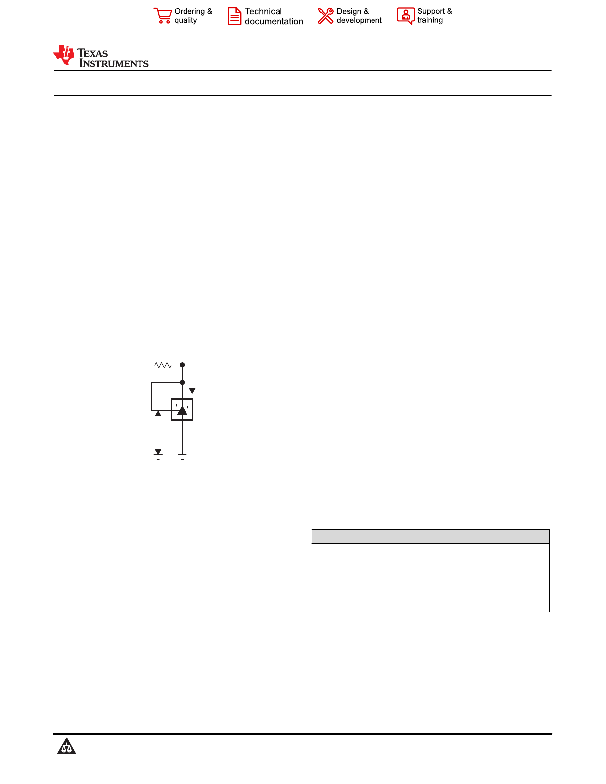
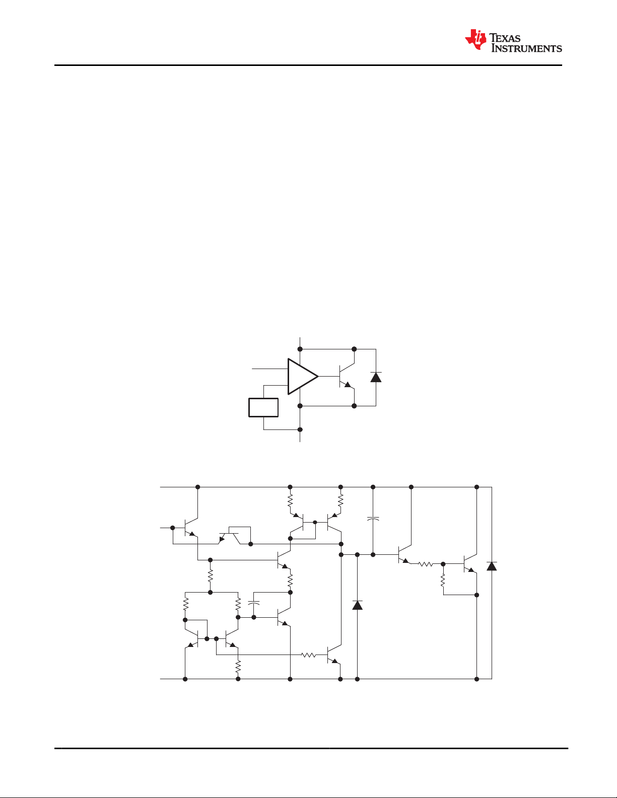
Simplified Schematic
from 0°C to 70°C, the TL43xxI devices are
characterized for operation from –40°C to 85°C, and
the TL43xxQ devices are characterized for operation
from –40°C to 125°C.
Device Information
PART NUMBER
TL43x
(1) For all available packages, see the orderable addendum at
the end of the data sheet.
An IMPORTANT NOTICE at the end of this data sheet addresses availability, warranty, changes, use in safety-critical applications,
intellectual property matters and other important disclaimers. PRODUCTION DATA.
(1)
PACKAGE (PIN) BODY SIZE (NOM)
SOT-23-3 (3) 2.90 mm × 1.30 mm
SOT-23-5 (5) 2.90 mm × 1.60 mm
SOIC (8) 4.90 mm × 3.90 mm
PDIP (8) 9.50 mm × 6.35 mm
SOP (8) 6.20 mm × 5.30 mm
Page 2

TL431, TL432
SLVS543Q – AUGUST 2004 – REVISED JULY 2022
www.ti.com
Table of Contents
1 Features............................................................................1
2 Applications..................................................................... 1
3 Description.......................................................................1
4 Revision History.............................................................. 2
5 Device Comparison Table...............................................3
6 Pin Configuration and Functions...................................4
7 Specifications.................................................................. 5
7.1 Absolute Maximum Ratings........................................ 5
7.2 ESD Ratings............................................................... 5
7.3 Thermal Information....................................................5
7.4 Recommended Operating Conditions.........................5
7.5 Electrical Characteristics, TL431C, TL432C............... 6
7.6 Electrical Characteristics, TL431I, TL432I.................. 7
7.7 Electrical Characteristics, TL431Q, TL432Q...............8
7.8 Electrical Characteristics, TL431AC, TL432AC.......... 9
7.9 Electrical Characteristics, TL431AI, TL432AI........... 10
7.10 Electrical Characteristics, TL431AQ, TL432AQ...... 11
7.11 Electrical Characteristics, TL431BC, TL432BC...... 12
7.12 Electrical Characteristics, TL431BI, TL432BI......... 13
7.13 Electrical Characteristics, TL431BQ, TL432BQ......14
8 Parameter Measurement Information.......................... 19
9 Detailed Description......................................................20
9.1 Overview................................................................... 20
9.2 Functional Block Diagram......................................... 20
9.3 Feature Description...................................................21
9.4 Device Functional Modes..........................................21
10 Applications and Implementation.............................. 22
10.1 Application Information........................................... 22
10.2 Typical Applications................................................ 22
10.3 System Examples................................................... 27
11 Power Supply Recommendations..............................30
12 Layout...........................................................................30
12.1 Layout Guidelines................................................... 30
12.2 Layout Example...................................................... 30
13 Device and Documentation Support..........................31
13.1 Device Nomenclature..............................................31
13.2 Related Links.......................................................... 31
13.3 Receiving Notification of Documentation Updates..31
13.4 Support Resources................................................. 31
13.5 Trademarks.............................................................31
13.6 Electrostatic Discharge Caution..............................32
13.7 Glossary..................................................................32
14 Mechanical, Packaging, and Orderable
Information.................................................................... 32
4 Revision History
Changes from Revision P (November 2018) to Revision Q (July 2022) Page
• Updated the numbering format for tables, figures, and cross-references throughout the document..................1
• Corrected the device names in the Pin Functions table..................................................................................... 4
Changes from Revision O (January 2015) to Revision P (November 2018) Page
• Added text to the Description section................................................................................................................. 1
• Added TL43x Device Comparison Table ........................................................................................................... 3
• Added TL43x Device Nomenclature section.....................................................................................................31
Changes from Revision N (January 2014) to Revision O (January 2015) Page
• Added Applications, Device Information table, Pin Functions table, ESD Ratings table, Thermal Information
table, Feature Description section, Device Functional Modes, Application and Implementation section, Power
Supply Recommendations section, Layout section, Device and Documentation Support section, and
Mechanical, Packaging, and Orderable Information section.............................................................................. 1
• Added Applications............................................................................................................................................. 1
• Moved Typical Characteristics into Specifications section. ............................................................................0
Changes from Revision M (July 2012) to Revision N (January 2014) Page
• Updated document formatting............................................................................................................................ 1
• Removed Ordering Information table..................................................................................................................4
• Added Application Note links............................................................................................................................ 22
2 Submit Document Feedback
Copyright © 2022 Texas Instruments Incorporated
Product Folder Links: TL431 TL432
Page 3

www.ti.com
5 Device Comparison Table
DEVICE PINOUT INITIAL ACCURACY OPERATING FREE-AIR TEMPERATURE (TA)
TL431
TL432
B: 0.5%
A: 1%
(Blank): 2%
SLVS543Q – AUGUST 2004 – REVISED JULY 2022
TL431, TL432
C: 0°C to 70°C
I: -40°C to 85°C
Q: -40°C to 125°C
Copyright © 2022 Texas Instruments Incorporated
Product Folder Links: TL431 TL432
Submit Document Feedback
3
Page 4
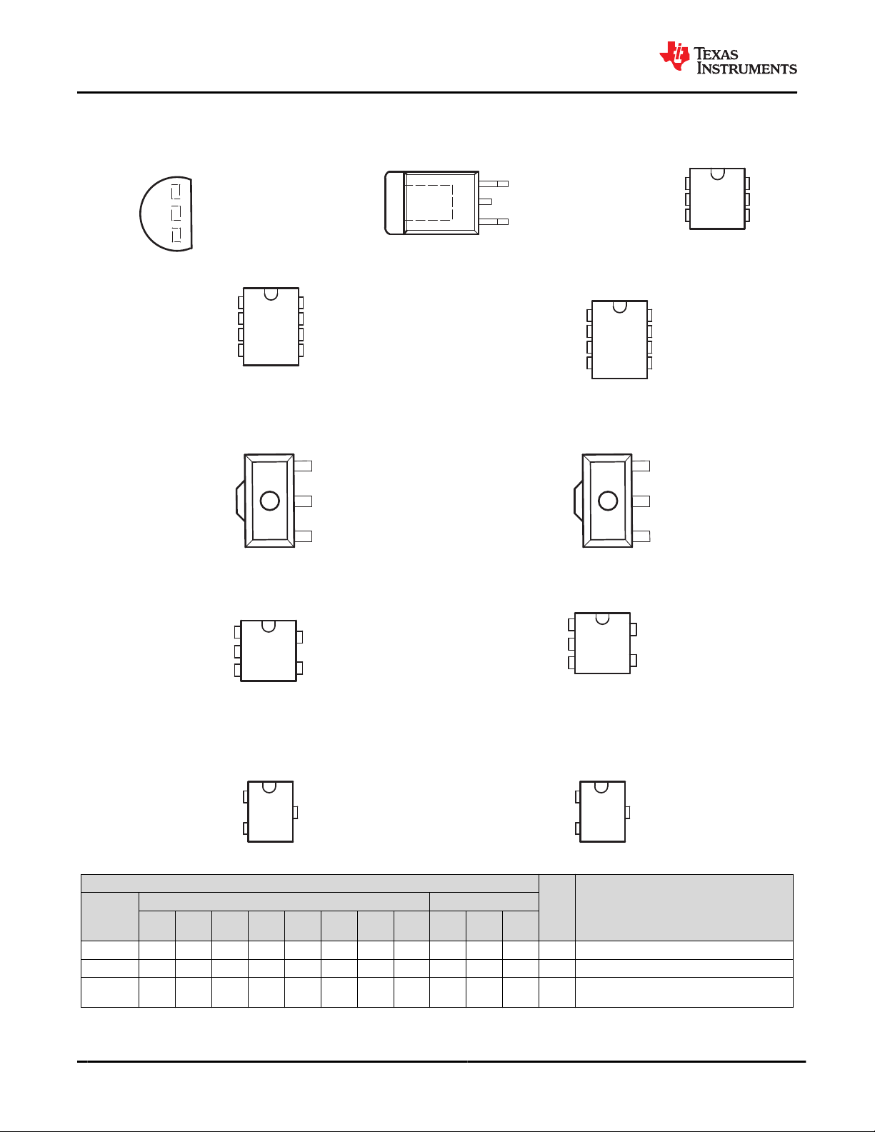
CATHODE
ANODE
REF
TL431 . . . KTP (PowerFLEX /TO-252) PACKAGE
(TOP VIEW)
ANODE
TL431A, TL431B . . . DCK (SC-70) PACKAGE
(TOP VIEW)
1
2
3
6
5
4
CATHODE
NC
REF
ANODE
NC
NC
NC − No internal connection
TL431, TL431A, TL431B . . . LP (TO-92/TO-226) PACKAGE
(TOP VIEW)
CATHODE
ANODE
REF
1
2
3
4
8
7
6
5
CATHODE
ANODE
ANODE
NC
REF
ANODE
ANODE
NC
TL431, TL431A, TL431B . . . D (SOIC) PACKAGE
(TOP VIEW)
1
2
3
4
8
7
6
5
CATHODE
NC
NC
NC
REF
NC
ANODE
NC
TL431, TL431A, TL431B . . . P (PDIP), PS (SOP),
OR PW (TSSOP) PACKAGE
(TOP VIEW)
NC − No internal connection
TL431, TL431A, TL431B . . . DBV (SOT-23-5) PACKAGE
(TOP VIEW)
1
2
3
5
4
NC
†
CATHODE
ANODE
REF
TL431, TL431A, TL431B . . . PK (SOT-89) PACKAGE
(TOP VIEW)
REF
ANODE
CATHODE
†
Pin 2 is attached to Substrate and must be
connected to ANODE or left open.
NC − No internal connection
TL432, TL432A, TL432B . . . DBV (SOT-23-5) PACKAGE
(TOP VIEW)
1
2
3
5
4
NC
ANODE
NC
REF
CATHODE
NC − No internal connection
TL431, TL431A, TL431B . . . DBZ (SOT-23-3) PACKAGE
(TOP VIEW)
TL432, TL432A, TL432B . . . DBZ (SOT-23-3) PACKAGE
(TOP VIEW)
NC − No internal connection
1
2
3
REF
CATHODE
ANODE
1
2
3
CATHODE
REF
ANODE
ANODE
TL432, TL432A, TL432B . . . PK (SOT-89) PACKAGE
(TOP VIEW)
REF
ANODE
CATHODE
ANODE
TL431, TL432
SLVS543Q – AUGUST 2004 – REVISED JULY 2022
6 Pin Configuration and Functions
www.ti.com
NAME
CATHODE 1 3 3 1 1 1 1 1 2 4 1 I/O Shunt Current/Voltage input
REF 2 4 1 8 8 3 3 3 1 5 3 I Threshold relative to common anode
ANODE 3 5 2
4 Submit Document Feedback
DBZ DBV PK D
2, 3,
6, 7
Table 6-1. Pin Functions
PIN
TL431x TL432x
P, PS
LP KTP DCK DBZ DBV PK
PW
6 2 2 6 3 2 2 O Common pin, normally connected to ground
Product Folder Links: TL431 TL432
TYPE DESCRIPTION
Copyright © 2022 Texas Instruments Incorporated
Page 5
www.ti.com
SLVS543Q – AUGUST 2004 – REVISED JULY 2022
7 Specifications
7.1 Absolute Maximum Ratings
TL431, TL432
over operating free-air temperature range (unless otherwise noted)
V
I
KA
I
I(ref)
T
T
KA
J
stg
Cathode voltage
Continuous cathode current range –100 150 mA
Reference input current range –0.05 10 mA
Operating virtual junction temperature 150 °C
Storage temperature range –65 150 °C
(1) Stresses beyond those listed under Absolute Maximum Ratings may cause permanent damage to the device. These are stress ratings
only, and functional operation of the device at these or any other conditions beyond those indicated under Recommended Operating
Conditions is not implied. Exposure to absolute-maximum-rated conditions for extended periods may affect device reliability.
(2) All voltage values are with respect to ANODE, unless otherwise noted.
(2)
7.2 ESD Ratings
Human-body model (HBM), per ANSI/ESDA/JEDEC JS-001
V
(ESD)
Electrostatic discharge
Charged-device model (CDM), per JEDEC specification JESD22-
(2)
C101
(1)
MIN MAX UNIT
37 V
VALUE UNIT
(1)
±2000
±1000
V
(1) JEDEC document JEP155 states that 500-V HBM allows safe manufacturing with a standard ESD control process. Manufacturing with
less than 500-V HBM is possible with the necessary precautions.
(2) JEDEC document JEP157 states that 250-V CDM allows safe manufacturing with a standard ESD control process. Manufacturing with
less than 250-V CDM is possible with the necessary precautions.
7.3 Thermal Information
TL43xx
(1)
8 PINS 6 PINS 5 PINS 3 PINS
85 149 97 95 259 206 206 140 52
57 65 39 46 87 131 76 55 9
UNITP PW D PS DCK DBV DBZ LP PK
°C/W
R
θJA
R
θJC(top)
THERMAL METRIC
Junction-to-ambient thermal
resistance
Junction-to-case (top) thermal
resistance
(1) For more information about traditional and new thermal metrics, see the IC Package Thermal Metrics application report (SPRA953).
7.4 Recommended Operating Conditions
(1)
See
MIN MAX UNIT
V
KA
I
KA
T
A
Cathode voltage V
ref
36 V
Cathode current 1 100 mA
TL43xxC 0 70
Operating free-air temperature
°CTL43xxI –40 85
TL43xxQ –40 125
(1) Maximum power dissipation is a function of T
temperature is PD = (T
Copyright © 2022 Texas Instruments Incorporated
– TA)/θJA. Operating at the absolute maximum TJ of 150°C can affect reliability.
J(max)
, θJA, and TA. The maximum allowable power dissipation at any allowable ambient
J(max)
Submit Document Feedback
Product Folder Links: TL431 TL432
5
Page 6
∆I
KA
∆V
KA
|z | =
KA
∆I
∆V
|z'| =
R2
R1
|z |
KA
(
1 +
(
TL431, TL432
SLVS543Q – AUGUST 2004 – REVISED JULY 2022
7.5 Electrical Characteristics, TL431C, TL432C
over recommended operating conditions, TA = 25°C (unless otherwise noted)
PARAMETER TEST CIRCUIT TEST CONDITIONS
V
ref
V
I(dev)
ΔV
ref
ΔV
KA
I
ref
I
I(dev)
I
min
I
off
|zKA| Dynamic impedance
Reference voltage See Figure 8-1 VKA = V
Deviation of reference input
voltage over full temperature
(1)
range
Ratio of change in reference
/
voltage to the change in
See Figure 8-1
See Figure 8-2 IKA = 10 mA
VKA = V
IKA = 10 mA,
, IKA = 10 mA 2440 2495 2550 mV
ref
,
ref
cathode voltage
Reference input current See Figure 8-2 IKA = 10 mA, R1 = 10 kΩ, R2 = ∞ 2 4 µA
Deviation of reference input
current over full temperature
(1)
range
Minimum cathode current for
regulation
Off-state cathode current See Figure 8-3 VKA = 36 V, V
(2)
See Figure 8-2 IKA = 10 mA, R1 = 10 kΩ, R2 = ∞ 0.4 1.2 µA
See Figure 8-1 VKA = V
See Figure 8-1
ref
= 0 0.1 1 µA
ref
VKA = V
, f ≤ 1 kHz,
ref
IKA = 1 mA to 100 mA
www.ti.com
TL431C, TL432C
MIN TYP MAX
SOT23-3 and TL432
devices
6 16
All other devices 4 25
ΔVKA = 10 V – V
ref
–1.4 –2.7
ΔVKA = 36 V – 10 V –1 –2
0.4 1 mA
0.2 0.5 Ω
UNIT
mV
mV/V
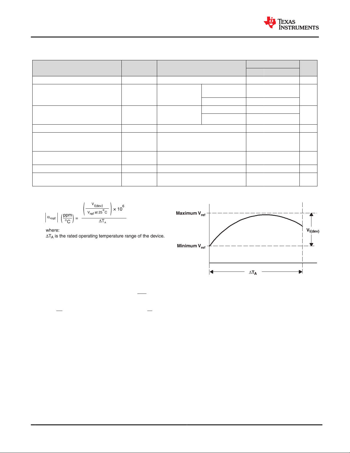
(1) The deviation parameters V
the rated temperature range. The average full-range temperature coefficient of the reference input voltage α
α
is positive or negative, depending on whether minimum V
Vref
ref(dev)
and I
are defined as the differences between the maximum and minimum values obtained over
ref(dev)
or maximum V
ref
, respectively, occurs at the lower temperature.
ref
is defined as:
Vref
(2) The dynamic impedance is defined as:
When the device is operating with two external resistors (see Figure 8-2), the total dynamic impedance of the circuit is given by:
which is approximately equal to
.
6 Submit Document Feedback
Copyright © 2022 Texas Instruments Incorporated
Product Folder Links: TL431 TL432
Page 7

www.ti.com
7.6 Electrical Characteristics, TL431I, TL432I
over recommended operating conditions, TA = 25°C (unless otherwise noted)
PARAMETER TEST CIRCUIT TEST CONDITIONS
V
ref
V
I(dev)
ΔV
ref
ΔV
KA
I
ref
I
I(dev)
I
min
I
off
|zKA| Dynamic impedance
Reference voltage See Figure 8-1 VKA = V
Deviation of reference input
voltage over full temperature
(1)
range
Ratio of change in reference
/
voltage to the change in
See Figure 8-1
See Figure 8-2 IKA = 10 mA
VKA = V
IKA = 10 mA
, IKA = 10 mA 2440 2495 2550 mV
ref
,
ref
cathode voltage
Reference input current See Figure 8-2 IKA = 10 mA, R1 = 10 kΩ, R2 = ∞ 2 4 µA
Deviation of reference input
current over full temperature
(1)
range
Minimum cathode current for
regulation
Off-state cathode current See Figure 8-3 VKA = 36 V, V
(2)
See Figure 8-2 IKA = 10 mA, R1 = 10 kΩ, R2 = ∞ 0.8 2.5 µA
See Figure 8-1 VKA = V
See Figure 8-1
ref
= 0 0.1 1 µA
ref
VKA = V
, f ≤ 1 kHz,
ref
IKA = 1 mA to 100 mA
SLVS543Q – AUGUST 2004 – REVISED JULY 2022
TL431, TL432
TL431I, TL432I
MIN TYP MAX
SOT23-3 and TL432
devices
All other devices 5 50
ΔVKA = 10 V – V
ref
ΔVKA = 36 V – 10 V –1 –2
14 34
–1.4 –2.7
0.4 1 mA
0.2 0.5 Ω
UNIT
mV
mV/V
Copyright © 2022 Texas Instruments Incorporated
Product Folder Links: TL431 TL432
Submit Document Feedback
7
Page 8
TL431, TL432
SLVS543Q – AUGUST 2004 – REVISED JULY 2022
7.7 Electrical Characteristics, TL431Q, TL432Q
over recommended operating conditions, TA = 25°C (unless otherwise noted)
PARAMETER TEST CIRCUIT TEST CONDITIONS
V
ref
V
I(dev)
ΔV
ref
ΔV
KA
I
ref
I
I(dev)
I
min
I
off
|zKA| Dynamic impedance
Reference voltage See Figure 8-1 VKA = V
, IKA = 10 mA 2440 2495 2550 mV
ref
Deviation of reference input
voltage over full temperature
(1)
range
Ratio of change in reference
/
voltage to the change in
See Figure 8-1 VKA = V
ref
See Figure 8-2 IKA = 10 mA
, IKA = 10 mA 14 34 mV
cathode voltage
Reference input current See Figure 8-2 IKA = 10 mA, R1 = 10 kΩ, R2 = ∞ 2 4 µA
Deviation of reference input
current over full temperature
(1)
range
Minimum cathode current for
regulation
Off-state cathode current See Figure 8-3 VKA = 36 V, V
(2)
See Figure 8-2 IKA = 10 mA, R1 = 10 kΩ, R2 = ∞ 0.8 2.5 µA
See Figure 8-1 VKA = V
See Figure 8-1
ref
= 0 0.1 1 µA
ref
VKA = V
, f ≤ 1 kHz,
ref
IKA = 1 mA to 100 mA
www.ti.com
TL431Q, TL432Q
MIN TYP MAX
ΔVKA = 10 V – V
ref
–1.4 –2.7
ΔVKA = 36 V – 10 V –1 –2
0.4 1 mA
0.2 0.5 Ω
UNIT
mV/V
8 Submit Document Feedback
Copyright © 2022 Texas Instruments Incorporated
Product Folder Links: TL431 TL432
Page 9

www.ti.com
7.8 Electrical Characteristics, TL431AC, TL432AC
over recommended operating conditions, TA = 25°C (unless otherwise noted)
PARAMETER TEST CIRCUIT TEST CONDITIONS
V
ref
V
I(dev)
ΔV
ref
ΔV
KA
I
ref
I
I(dev)
I
min
I
off
|zKA| Dynamic impedance
Reference voltage See Figure 8-1 VKA = V
Deviation of reference input
voltage over full temperature
(1)
range
Ratio of change in reference
/
voltage to the change in
See Figure 8-1
See Figure 8-2 IKA = 10 mA
VKA = V
IKA = 10 mA
, IKA = 10 mA 2470 2495 2520 mV
ref
,
ref
cathode voltage
Reference input current See Figure 8-2 IKA = 10 mA, R1 = 10 kΩ, R2 = ∞ 2 4 µA
Deviation of reference input
current over full temperature
(1)
range
Minimum cathode current for
regulation
Off-state cathode current See Figure 8-3 VKA = 36 V, V
(2)
See Figure 8-2 IKA = 10 mA, R1 = 10 kΩ, R2 = ∞ 0.8 1.2 µA
See Figure 8-1 VKA = V
See Figure 8-1
ref
= 0 0.1 0.5 µA
ref
VKA = V
, f ≤ 1 kHz,
ref
IKA = 1 mA to 100 mA
SLVS543Q – AUGUST 2004 – REVISED JULY 2022
TL431, TL432
TL431AC, TL432AC
MIN TYP MAX
SOT23-3 and TL432
devices
All other devices 4 25
ΔVKA = 10 V – V
ref
ΔVKA = 36 V – 10 V –1 –2
6 16
–1.4 –2.7
0.4 0.6 mA
0.2 0.5 Ω
UNIT
mV
mV/V
Copyright © 2022 Texas Instruments Incorporated
Product Folder Links: TL431 TL432
Submit Document Feedback
9
Page 10
TL431, TL432
SLVS543Q – AUGUST 2004 – REVISED JULY 2022
7.9 Electrical Characteristics, TL431AI, TL432AI
over recommended operating conditions, TA = 25°C (unless otherwise noted)
PARAMETER TEST CIRCUIT TEST CONDITIONS
V
ref
V
I(dev)
ΔV
ref
ΔV
KA
I
ref
I
I(dev)
I
min
I
off
|zKA| Dynamic impedance
Reference voltage See Figure 8-1 VKA = V
Deviation of reference input
voltage over full temperature
(1)
range
Ratio of change in reference
/
voltage to the change in
See Figure 8-1
See Figure 8-2 IKA = 10 mA
VKA = V
IKA = 10 mA
, IKA = 10 mA 2470 2495 2520 mV
ref
,
ref
cathode voltage
Reference input current See Figure 8-2 IKA = 10 mA, R1 = 10 kΩ, R2 = ∞ 2 4 µA
Deviation of reference input
current over full temperature
(1)
range
Minimum cathode current for
regulation
Off-state cathode current See Figure 8-3 VKA = 36 V, V
(2)
See Figure 8-2 IKA = 10 mA, R1 = 10 kΩ, R2 = ∞ 0.8 2.5 µA
See Figure 8-1 VKA = V
See Figure 8-1
ref
= 0 0.1 0.5 µA
ref
VKA = V
, f ≤ 1 kHz,
ref
IKA = 1 mA to 100 mA
www.ti.com
TL431AI, TL432AI
MIN TYP MAX
SOT23-3 and TL432
devices
14 34
All other devices 5 50
ΔVKA = 10 V – V
ref
–1.4 –2.7
ΔVKA = 36 V – 10 V –1 –2
0.4 0.7 mA
0.2 0.5 Ω
UNIT
mV
mV/V
10 Submit Document Feedback
Copyright © 2022 Texas Instruments Incorporated
Product Folder Links: TL431 TL432
Page 11
www.ti.com
7.10 Electrical Characteristics, TL431AQ, TL432AQ
over recommended operating conditions, TA = 25°C (unless otherwise noted)
PARAMETER TEST CIRCUIT TEST CONDITIONS
V
ref
V
I(dev)
ΔV
ref
ΔV
KA
I
ref
I
I(dev)
I
min
I
off
|zKA| Dynamic impedance
Reference voltage See Figure 8-1 VKA = V
, IKA = 10 mA 2470 2495 2520 mV
ref
Deviation of reference input
voltage over full temperature
(1)
range
Ratio of change in reference
/
voltage to the change in
See Figure 8-1 VKA = V
ref
See Figure 8-2 IKA = 10 mA
, IKA = 10 mA 14 34 mV
cathode voltage
Reference input current See Figure 8-2 IKA = 10 mA, R1 = 10 kΩ, R2 = ∞ 2 4 µA
Deviation of reference input
current over full temperature
(1)
range
Minimum cathode current for
regulation
Off-state cathode current See Figure 8-3 VKA = 36 V, V
(2)
See Figure 8-2 IKA = 10 mA, R1 = 10 kΩ, R2 = ∞ 0.8 2.5 µA
See Figure 8-1 VKA = V
See Figure 8-1
ref
= 0 0.1 0.5 µA
ref
VKA = V
, f ≤ 1 kHz,
ref
IKA = 1 mA to 100 mA
SLVS543Q – AUGUST 2004 – REVISED JULY 2022
TL431, TL432
TL431AQ, TL432AQ
MIN TYP MAX
ΔVKA = 10 V – V
ref
ΔVKA = 36 V – 10 V –1 –2
–1.4 –2.7
0.4 0.7 mA
0.2 0.5 Ω
UNIT
mV/V
Copyright © 2022 Texas Instruments Incorporated
Product Folder Links: TL431 TL432
Submit Document Feedback
11
Page 12

TL431, TL432
SLVS543Q – AUGUST 2004 – REVISED JULY 2022
7.11 Electrical Characteristics, TL431BC, TL432BC
over recommended operating conditions, TA = 25°C (unless otherwise noted)
PARAMETER TEST CIRCUIT TEST CONDITIONS
V
ref
V
I(dev)
ΔV
ref
ΔV
KA
I
ref
I
I(dev)
I
min
I
off
|zKA| Dynamic impedance
Reference voltage See Figure 8-1 VKA = V
, IKA = 10 mA 2483 2495 2507 mV
ref
Deviation of reference input
voltage over full temperature
(1)
range
Ratio of change in reference
/
voltage to the change in
See Figure 8-1 VKA = V
ref
See Figure 8-2 IKA = 10 mA
, IKA = 10 mA 6 16 mV
cathode voltage
Reference input current See Figure 8-2 IKA = 10 mA, R1 = 10 kΩ, R2 = ∞ 2 4 µA
Deviation of reference input
current over full temperature
(1)
range
Minimum cathode current for
regulation
Off-state cathode current See Figure 8-3 VKA = 36 V, V
(2)
See Figure 8-2 IKA = 10 mA, R1 = 10 kΩ, R2 = ∞ 0.8 1.2 µA
See Figure 8-1 VKA = V
See Figure 8-1
ref
= 0 0.1 0.5 µA
ref
VKA = V
, f ≤ 1 kHz,
ref
IKA = 1 mA to 100 mA
www.ti.com
TL431BC, TL432BC
MIN TYP MAX
ΔVKA = 10 V – V
ref
–1.4 –2.7
ΔVKA = 36 V – 10 V – –2
0.4 0.6 mA
0.2 0.5 Ω
UNIT
mV/V
12 Submit Document Feedback
Copyright © 2022 Texas Instruments Incorporated
Product Folder Links: TL431 TL432
Page 13

www.ti.com
7.12 Electrical Characteristics, TL431BI, TL432BI
over recommended operating conditions, TA = 25°C (unless otherwise noted)
PARAMETER TEST CIRCUIT TEST CONDITIONS
V
ref
V
I(dev)
ΔV
ref
ΔV
KA
I
ref
I
I(dev)
I
min
I
off
|zKA| Dynamic impedance
Reference voltage See Figure 8-1 VKA = V
, IKA = 10 mA 2483 2495 2507 mV
ref
Deviation of reference input
voltage over full temperature
(1)
range
Ratio of change in reference
/
voltage to the change in
See Figure 8-1 VKA = V
ref
See Figure 8-2 IKA = 10 mA
, IKA = 10 mA 14 34 mV
cathode voltage
Reference input current See Figure 8-2 IKA = 10 mA, R1 = 10 kΩ, R2 = ∞ 2 4 µA
Deviation of reference input
current over full temperature
(1)
range
Minimum cathode current for
regulation
Off-state cathode current See Figure 8-3 VKA = 36 V, V
(2)
See Figure 8-2 IKA = 10 mA, R1 = 10 kΩ, R2 = ∞ 0.8 2.5 µA
See Figure 8-1 VKA = V
See Figure 8-1
ref
= 0 0.1 0.5 µA
ref
VKA = V
, f ≤ 1 kHz,
ref
IKA = 1 mA to 100 mA
SLVS543Q – AUGUST 2004 – REVISED JULY 2022
TL431, TL432
TL431BI, TL432BI
MIN TYP MAX
ΔVKA = 10 V – V
ref
ΔVKA = 36 V – 10 V –1 –2
–1.4 –2.7
0.4 0.7 mA
0.2 0.5 Ω
UNIT
mV/V
Copyright © 2022 Texas Instruments Incorporated
Product Folder Links: TL431 TL432
Submit Document Feedback
13
Page 14

TL431, TL432
SLVS543Q – AUGUST 2004 – REVISED JULY 2022
7.13 Electrical Characteristics, TL431BQ, TL432BQ
over recommended operating conditions, TA = 25°C (unless otherwise noted)
PARAMETER TEST CIRCUIT TEST CONDITIONS
V
ref
V
I(dev)
ΔV
ref
ΔV
KA
I
ref
I
I(dev)
I
min
I
off
|zKA| Dynamic impedance
Reference voltage See Figure 8-1 VKA = V
, IKA = 10 mA 2483 2495 2507 mV
ref
Deviation of reference input
voltage over full temperature
(1)
range
Ratio of change in reference
/
voltage to the change in
See Figure 8-1 VKA = V
ref
See Figure 8-2 IKA = 10 mA
, IKA = 10 mA 14 34 mV
cathode voltage
Reference input current See Figure 8-2 IKA = 10 mA, R1 = 10 kΩ, R2 = ∞ 2 4 µA
Deviation of reference input
current over full temperature
(1)
range
Minimum cathode current for
regulation
Off-state cathode current See Figure 8-3 VKA = 36 V, V
(2)
See Figure 8-2 IKA = 10 mA, R1 = 10 kΩ, R2 = ∞ 0.8 2.5 µA
See Figure 8-1 VKA = V
See Figure 8-1
ref
= 0 0.1 0.5 µA
ref
VKA = V
, f ≤ 1 kHz,
ref
IKA = 1 mA to 100 mA
www.ti.com
TL431BQ, TL432BQ
MIN TYP MAX
ΔVKA = 10 V – V
ref
–1.4 –2.7
ΔVKA = 36 V – 10 V –1 –2
0.4 0.7 mA
0.2 0.5 Ω
UNIT
mV/V
14 Submit Document Feedback
Copyright © 2022 Texas Instruments Incorporated
Product Folder Links: TL431 TL432
Page 15
2500
2480
2420
2400
−75 −50 −25 0 25 50 75
2540
2580
2600
100 125
2460
2560
2520
2440
T
− Free-Air Temperature − °C
V
ref
= 2495 mV
V
ref
= 2440 mV
VKA= V
ref
IKA= 10 mA
V
ref
= 2550 mV
− Reference Voltage − mV
V
ref
3
2
1
0
−75 −25 0 50
4
5
100 125
−50 25 75
T
− Free-Air Temperature − °C
R1 = 10 kΩ
R2 =∞
IKA= 10 mA
− Reference Current −ref
I
µA
25
0
−50
−75
−100
125
−25
−2 −1 0 1
75
50
100
150
2 3
V
− Cathode Voltage − V
VKA= V
ref
TA= 25°C
− Cathode Current − mA
I
KA
400
200
0
−200
−1 0 1
600
800
2 3
VKA= V
ref
TA= 25°C
VKA− Cathode Voltage − V
I
min
− Cathode Current −I
KA
Aµ
1.5
1
0.5
0
−75 −25 0 50
− Off-State Cathode Current −
2
2.5
100 125−50 25 75
I
off
µA
T
− Free-Air Temperature − °C
VKA= 36 V
V
ref
= 0
16
−1.15
−1.25
−1.35
−1.45
−1.05
− 0.95
− 0.85
T
− Free-Air Temperature − °C
−75 −25 0 50 100 125−50 25 75
VKA= 3 V to 36 V
− mV/V
∆V
ref
∆V
KA
/
16
www.ti.com
SLVS543Q – AUGUST 2004 – REVISED JULY 2022
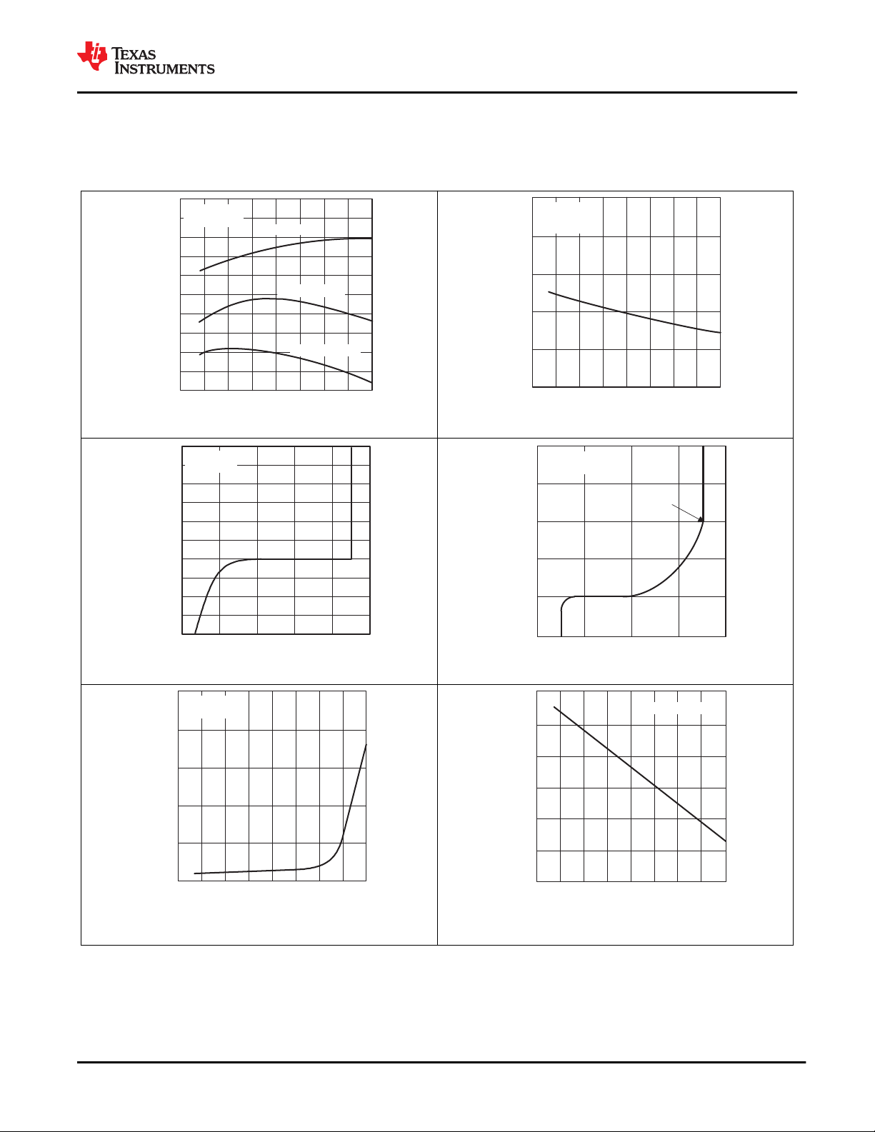
Typical Characteristics
Data at high and low temperatures are applicable only within the recommended operating free-air temperature ranges of the
various devices.
TL431, TL432
Figure 7-1. Reference Voltage vs Free-Air Temperature
Figure 7-3. Cathode Current vs Cathode Voltage
Figure 7-2. Reference Current vs Free-Air Temperature
Figure 7-4. Cathode Current vs Cathode Voltage
Figure 7-5. Off-State Cathode Current vs Free-Air Temperature
Copyright © 2022 Texas Instruments Incorporated
Figure 7-6. Ratio of Delta Reference Voltage to Delta Cathode
Product Folder Links: TL431 TL432
Voltage vs Free-Air Temperature
Submit Document Feedback
15
Page 16
180
140
120
100
10 100 1 k
220
240
f − Frequency − Hz
260
10 k 100 k
200
160
− Equivalent Input Noise V oltage − nV/
Hz
V
n
IO= 10 mA
TA= 25°C
16
−1
−2
−4
−5
−6
3
−3
0 1 2 3 4 5 6
1
0
2
4
7 8 9 10
5
6
t − Time − s
f = 0.1 to 10 Hz
IKA= 10 mA
TA= 25°C
− Equivalent Input Noise V oltage − µ V
V
n
19.1 V
V
CC
TLE2027
TLE2027
AV= 10 V/mV
V
EE
0.1 µF
160 kΩ
820 Ω
(DUT)
TL431
16 Ω
910 Ω
2000 µF
1 kΩ
V
EE
V
CC
1 µF
16 kΩ 16 kΩ
1 µF
33 kΩ
33 kΩ
AV= 2 V/V
22 µF
500 µF
To
Oscilloscope
+
−
+
−
TL431, TL432
SLVS543Q – AUGUST 2004 – REVISED JULY 2022
www.ti.com
Typical Characteristics
Data at high and low temperatures are applicable only within the recommended operating free-air temperature ranges of the
various devices.
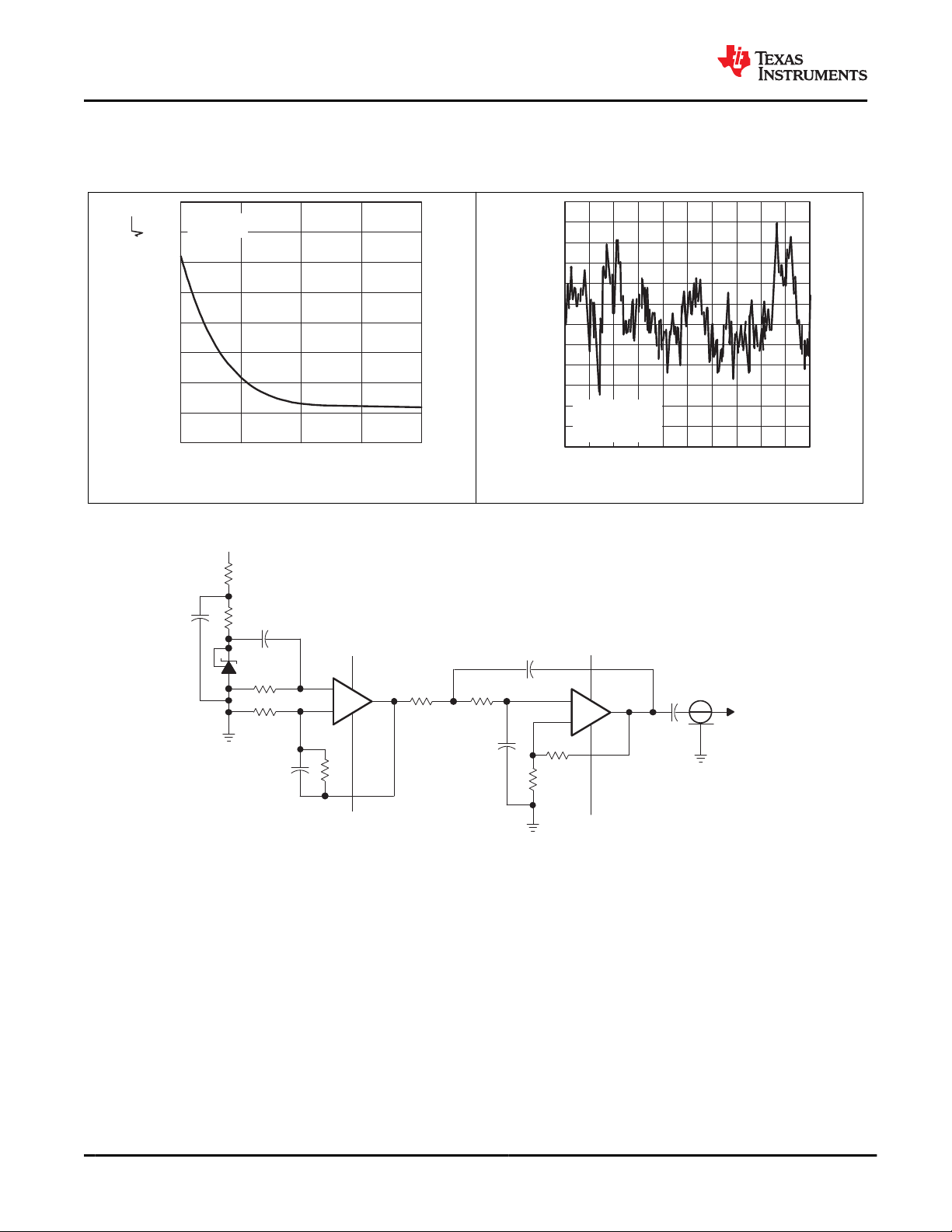
Figure 7-7. Equivalent Input Noise Voltage vs Frequency
Figure 7-9. Test Circuit for Equivalent Input Noise Voltage Over a 10-S Period
Figure 7-8. Equivalent Input Noise Voltage Over a 10-S Period
16 Submit Document Feedback
Product Folder Links: TL431 TL432
Copyright © 2022 Texas Instruments Incorporated
Page 17
1 k 10 k 100 k 1 M 10 M
0
10
20
30
50
60
40
f − Frequency − Hz
IKA= 10 mA
TA= 25°C
− Small-Signal V oltage Amplification − dBA
V
9 µF
GND
Output
232 Ω
8.25 kΩ
I
KA
15 kΩ
+
−
IKA= 10 mA
TA= 25°C
0.1
1 k 10 k 100 k 1 M 10 M
1
f − Frequency − Hz
10
100
IKA= 10 mA
TA= 25°C
− Reference Impedance −
KA
|z | Ω
1 kΩ
50 Ω
GND
Output
I
KA
+
−
3
2
1
0
−1 0 1 2 3 4
Input and Output V oltage − V
4
5
6
5 6 7
Input
Output
TA= 25°C
t − Time − µs
220 Ω
50 Ω
GND
Output
Pulse
Generator
f = 100 kHz
www.ti.com
SLVS543Q – AUGUST 2004 – REVISED JULY 2022
Typical Characteristics
Data at high and low temperatures are applicable only within the recommended operating free-air temperature ranges of the
various devices.
TL431, TL432
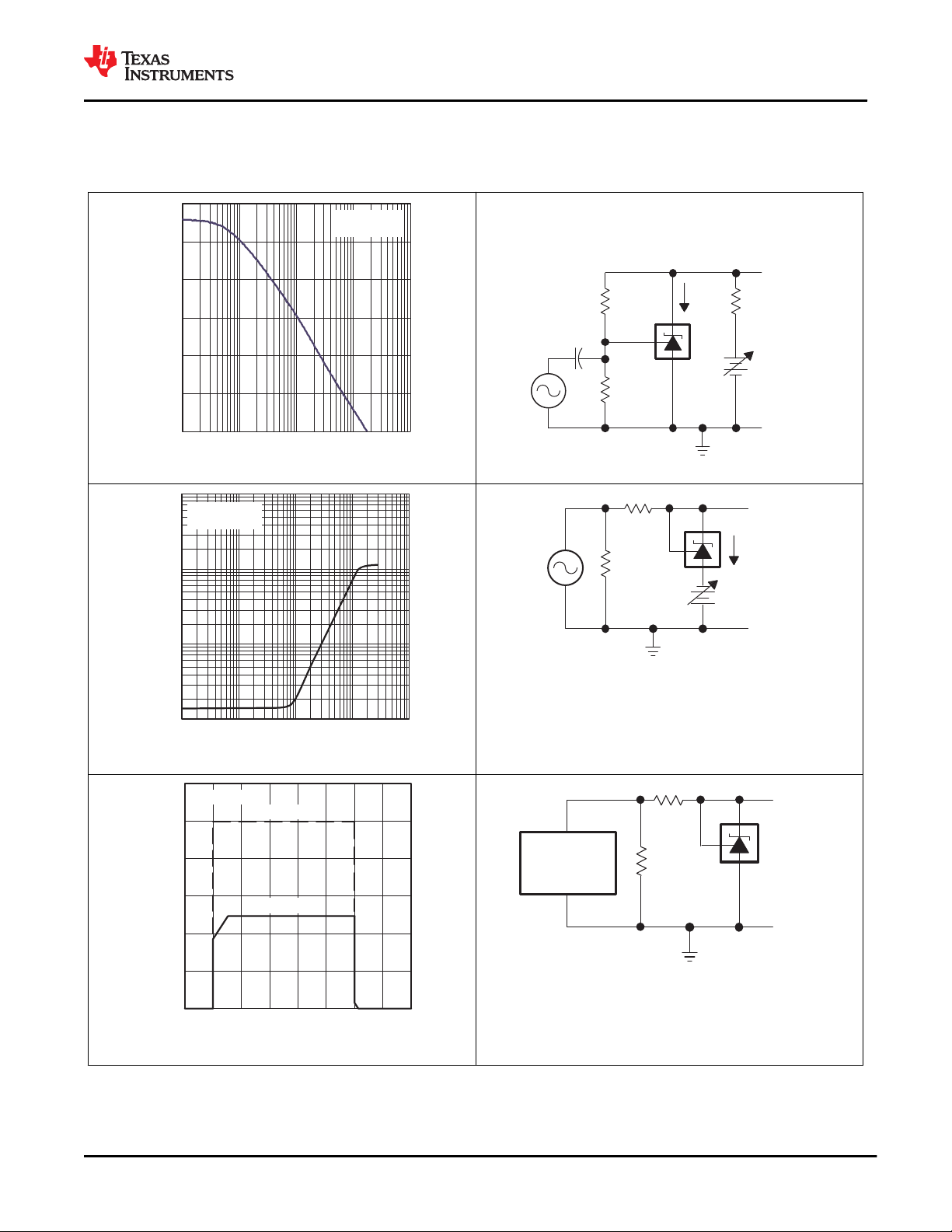
Figure 7-10. Small-Signal Voltage Amplification vs Frequency
Figure 7-12. Reference Impedance vs Frequency
Figure 7-11. Test Circuit for Voltage Amplification
Figure 7-13. Test Circuit for Reference Impedance
Copyright © 2022 Texas Instruments Incorporated
Figure 7-14. Pulse Response
Figure 7-15. Test Circuit for Pulse Response
Product Folder Links: TL431 TL432
Submit Document Feedback
17
Page 18
50
40
10
0
0.001 0.01 0.1 1
70
90
100
10
30
80
60
20
TA= 25°C
B
Stable
Stable
A VKA= V
ref
B VKA= 5 V
C VKA= 10 V
D VKA= 15 V
f
C
− Load Capacitance − µF
A
C
D
− Cathode Current − mA
I
KA
150 Ω
I
KA
R1 = 10 kΩ
R2
C
L
V
BATT
I
KA
C
L
V
BATT
150 Ω
TEST CIRCUIT FOR CURVE A
TEST CIRCUIT FOR CURVES B, C, AND D
+
−
+
−
50
40
10
0
0.001 0.01 0.1 1
70
90
100
10
30
80
60
20
Stable
A VKA= V
ref
B VKA= 5 V
C VKA= 10 V
D VKA= 15 V
f
C
− Load Capacitance − µF
A
C
D
− Cathode Current − mA
I
KA
B
A
TA= 25°C
Stable
B
150
Ω
I
KA
R1 = 10 kΩ
R2
C
L
V
BATT
I
KA
C
L
V
BATT
150 Ω
TEST CIRCUIT FOR CURVE A
TEST CIRCUIT FOR CURVES B, C, AND D
+
−
+
−
TL431, TL432
SLVS543Q – AUGUST 2004 – REVISED JULY 2022
www.ti.com
Typical Characteristics
Data at high and low temperatures are applicable only within the recommended operating free-air temperature ranges of the
various devices.
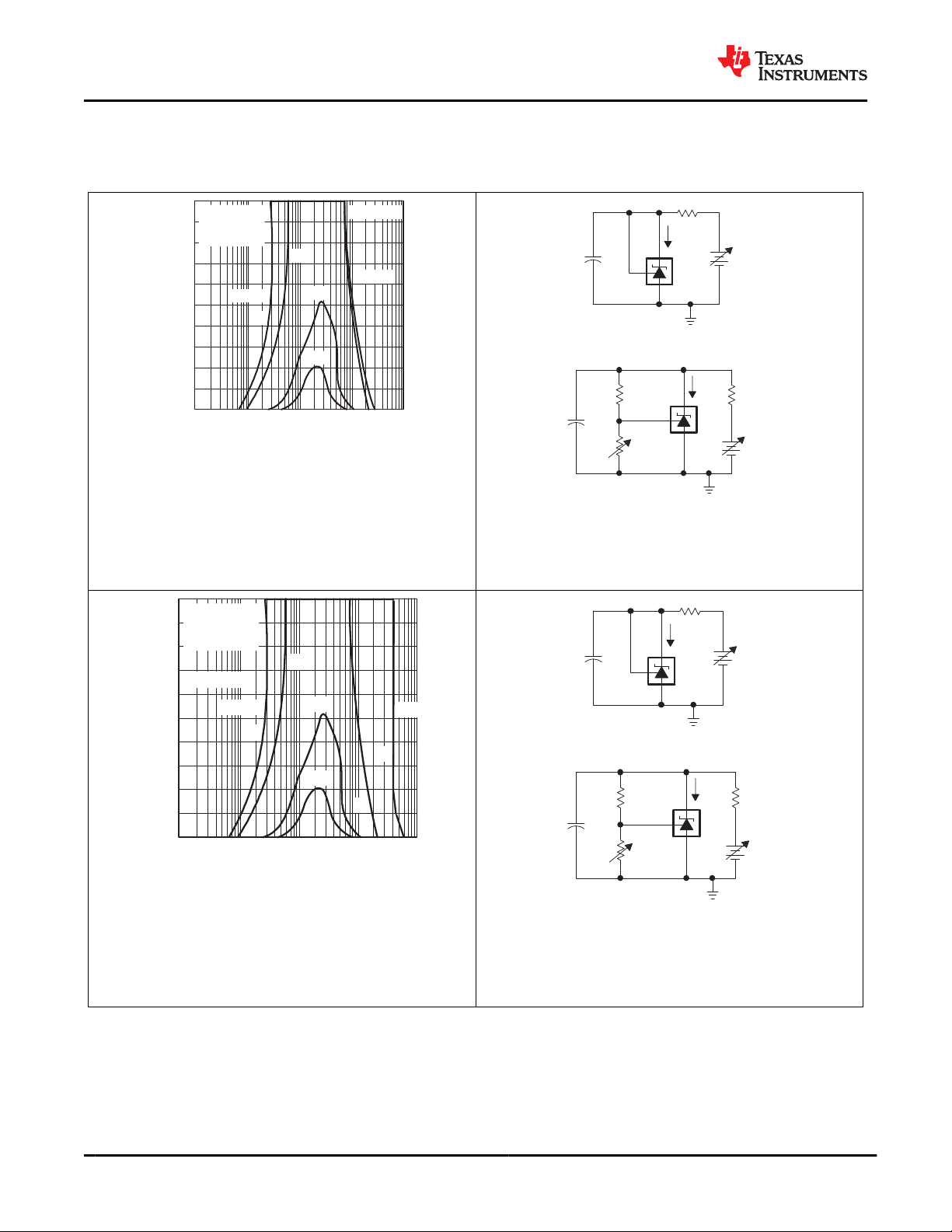
The areas under the curves represent conditions that may
cause the device to oscillate. For curves B, C, and D, R2 and
V+ are adjusted to establish the initial VKA and IKA conditions,
with CL = 0. V
ranges of stability.
Figure 7-16. Stability Boundary Conditions for All TL431 and
TL431A Devices (Except for SOT23-3, SC-70, and Q-Temp
and CL then are adjusted to determine the
BATT
Devices)
Figure 7-17. Test Circuits for Stability Boundary Conditions
The areas under the curves represent conditions that may
cause the device to oscillate. For curves B, C, and D, R2 and
V+ are adjusted to establish the initial VKA and IKA conditions,
with CL = 0. V
ranges of stability.
18 Submit Document Feedback
Figure 7-18. Stability Boundary Conditions for All TL431B,
TL432, SOT-23, SC-70, and Q-Temp Devices
and CL then are adjusted to determine the
BATT
Figure 7-19. Test Circuit for Stability Boundary Conditions
Copyright © 2022 Texas Instruments Incorporated
Product Folder Links: TL431 TL432
Page 19
V
ref
Input
V
KA
I
KA
I
ref
I
KA
V
KA
Input
V
ref
R1
R2
KA ref ref
R1
V = V 1 + + I × R1
R2
æ ö
ç ÷
è ø
I
off
V
KA
Input
www.ti.com
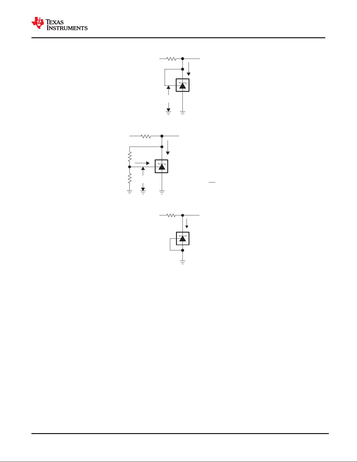
8 Parameter Measurement Information
SLVS543Q – AUGUST 2004 – REVISED JULY 2022
TL431, TL432
Figure 8-1. Test Circuit for VKA = V
Figure 8-2. Test Circuit for VKA > V
Figure 8-3. Test Circuit for I
off
ref
ref
Copyright © 2022 Texas Instruments Incorporated
Submit Document Feedback
19
Product Folder Links: TL431 TL432
Page 20
CATHODE
REF
ANODE
+
_
V
ref
ANODE
REF
CATHODE
2.4 kΩ
7.2 kΩ
3.28 kΩ
20 pF
4 kΩ
1 kΩ
800 Ω
800 Ω
800 Ω
20 pF
150 Ω
10 kΩ
TL431, TL432
SLVS543Q – AUGUST 2004 – REVISED JULY 2022
www.ti.com
9 Detailed Description
9.1 Overview
This standard device has proven ubiquity and versatility across a wide range of applications, ranging from power
to signal path. This is due to it's key components containing an accurate voltage reference & opamp, which are
very fundamental analog building blocks. TL43xx is used in conjunction with it's key components to behave as a
single voltage reference, error amplifier, voltage clamp or comparator with integrated reference.
TL43xx can be operated and adjusted to cathode voltages from 2.5V to 36V, making this part optimum for a
wide range of end equipments in industrial, auto, telecom & computing. In order for this device to behave as a
shunt regulator or error amplifier, >1mA (I
feedback can be applied from the Cathode and Ref pins to create a replica of the internal reference voltage.
Various reference voltage options can be purchased with initial tolerances (at 25°C) of 0.5%, 1%, and 2%. These
reference options are denoted by B (0.5%), A (1.0%) and blank (2.0%) after the TL431 or TL432. TL431 &
TL432 are both functionaly, but have separate pinout options.
The TL43xxC devices are characterized for operation from 0°C to 70°C, the TL43xxI devices are characterized
for operation from –40°C to 85°C, and the TL43xxQ devices are characterized for operation from –40°C to
125°C.
9.2 Functional Block Diagram
(max)) must be supplied in to the cathode pin. Under this condition,
min
20 Submit Document Feedback
Figure 9-1. Equivalent Schematic
Figure 9-2. Detailed Schematic
Product Folder Links: TL431 TL432
Copyright © 2022 Texas Instruments Incorporated
Page 21

www.ti.com
SLVS543Q – AUGUST 2004 – REVISED JULY 2022
TL431, TL432
9.3 Feature Description
TL43xx consists of an internal reference and amplifier that outputs a sink current base on the difference between
the reference pin and the virtual internal pin. The sink current is produced by the internal Darlington pair, shown
in the above schematic (Figure 9-2). A Darlington pair is used in order for this device to be able to sink a
maximum current of 100 mA.
When operated with enough voltage headroom (≥ 2.5 V) and cathode current (IKA), TL431 forces the reference
pin to 2.5 V. However, the reference pin can not be left floating, as it needs I
≥ 4 µA (please see Electrical
REF
Characteristics, TL431C, TL432C). This is because the reference pin is driven into an npn, which needs base
current in order operate properly.
When feedback is applied from the Cathode and Reference pins, TL43xx behaves as a Zener diode, regulating
to a constant voltage dependent on current being supplied into the cathode. This is due to the internal amplifier
and reference entering the proper operating regions. The same amount of current needed in the above feedback
situation must be applied to this device in open loop, servo or error amplifying implementations in order for it to
be in the proper linear region giving TL43xx enough gain.
Unlike many linear regulators, TL43xx is internally compensated to be stable without an output capacitor
between the cathode and anode. However, if it is desired to use an output capacitor Figure 9-2 can be used as a
guide to assist in choosing the correct capacitor to maintain stability.
9.4 Device Functional Modes
9.4.1 Open Loop (Comparator)
When the cathode/output voltage or current of TL43xx is not being fed back to the reference/input pin in any
form, this device is operating in open loop. With proper cathode current (Ika) applied to this device, TL43xx
will have the characteristics shown in Figure 9-1. With such high gain in this configuration, TL43xx is typically
used as a comparator. With the reference integrated makes TL43xx the prefered choice when users are trying to
monitor a certain level of a single signal.
9.4.2 Closed Loop
When the cathode/output voltage or current of TL43xx is being fed back to the reference/input pin in any form,
this device is operating in closed loop. The majority of applications involving TL43xx use it in this manner to
regulate a fixed voltage or current. The feedback enables this device to behave as an error amplifier, computing
a portion of the output voltage and adjusting it to maintain the desired regulation. This is done by relating the
output voltage back to the reference pin in a manner to make it equal to the internal reference voltage, which can
be accomplished via resistive or direct feedback.
Copyright © 2022 Texas Instruments Incorporated
Product Folder Links: TL431 TL432
Submit Document Feedback
21
Page 22
+
2.5V
CATHODE
ANODE
REF
V
IN
Vout
Vsup
Rsup
R1
R2
V
L
R
IN
TL431, TL432
SLVS543Q – AUGUST 2004 – REVISED JULY 2022
www.ti.com
10 Applications and Implementation
Note
Information in the following applications sections is not part of the TI component specification, and
TI does not warrant its accuracy or completeness. TI’s customers are responsible for determining
suitability of components for their purposes. Customers should validate and test their design
implementation to confirm system functionality.
10.1 Application Information
As this device has many applications and setups, there are many situations that this datasheet can not
characterize in detail. The linked application notes will help the designer make the best choices when using
this part.
Application note Understanding Stability Boundary Conditions Charts in TL431, TL432 Data Sheet (SLVA482)
will provide a deeper understanding of this devices stability characteristics and aid the user in making the right
choices when choosing a load capacitor. Application note Setting the Shunt Voltage on an Adjustable Shunt
Regulator (SLVA445) assists designers in setting the shunt voltage to achieve optimum accuracy for this device.
10.2 Typical Applications
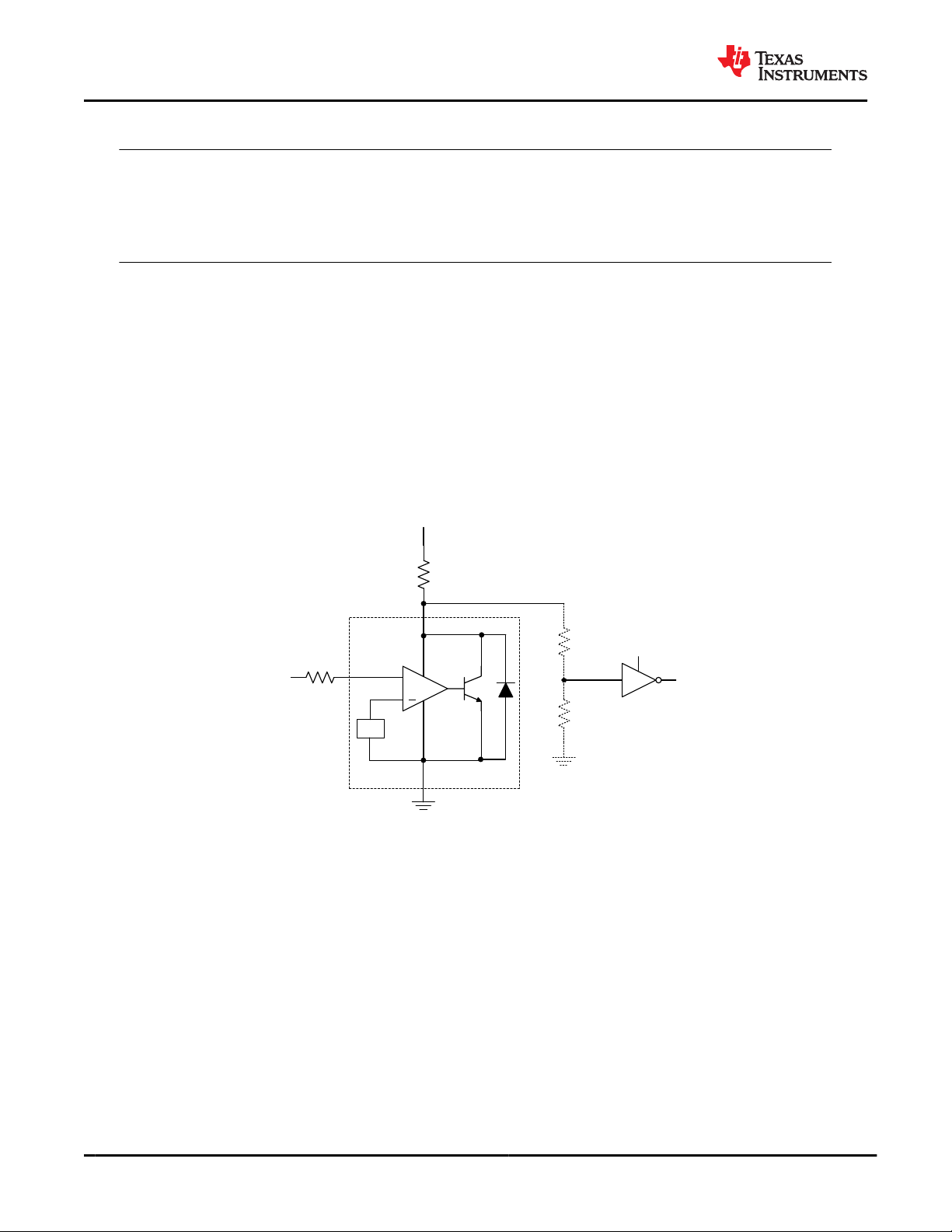
10.2.1 Comparator With Integrated Reference
Figure 10-1. Comparator Application Schematic
22 Submit Document Feedback
Product Folder Links: TL431 TL432
Copyright © 2022 Texas Instruments Incorporated
Page 23
www.ti.com
SLVS543Q – AUGUST 2004 – REVISED JULY 2022
10.2.1.1 Design Requirements
For this design example, use the parameters listed in Table 10-1 as the input parameters.
Table 10-1. Design Parameters
DESIGN PARAMETER EXAMPLE VALUE
Input Voltage Range 0 V to 5 V
Input Resistance 10 kΩ
Supply Voltage 24 V
Cathode Current (Ik) 5 mA
Output Voltage Level ~2 V – V
Logic Input Thresholds VIH/VIL V
L
10.2.1.2 Detailed Design Procedure
When using TL431 as a comparator with reference, determine the following:
• Input Voltage Range
• Reference Voltage Accuracy
• Output logic input high and low level thresholds
• Current Source resistance
10.2.1.2.1 Basic Operation
TL431, TL432
SUP
In the configuration shown in Figure 10-1 TL431 will behave as a comparator, comparing the V
pin voltage
REF
to the internal virtual reference voltage. When provided a proper cathode current (IK), TL43xx will have enough
open loop gain to provide a quick response. This can be seen in Figure 10-2, where the R
µA) situation responds much slower than R
(I
) being 1 mA, operation below that could result in low gain, leading to a slow response.
MIN
10.2.1.2.1.1 Overdrive
=1 kΩ (IKA=5 mA). With the TL43xx's max Operating Current
SUP
=10 kΩ (IKA=500
SUP
Slow or inaccurate responses can also occur when the reference pin is not provided enough overdrive voltage.
This is the amount of voltage that is higher than the internal virtual reference. The internal virtual reference
voltage will be within the range of 2.5 V ±(0.5%, 1.0% or 1.5%) depending on which version is being used. The
more overdrive voltage provided, the faster the TL431 will respond.
For applications where TL431 is being used as a comparator, it is best to set the trip point to greater than the
positive expected error (i.e. +1.0% for the A version). For fast response, setting the trip point to >10% of the
internal V
should suffice.
REF
For minimal voltage drop or difference from Vin to the ref pin, it is recommended to use an input resistor <10kΩ
to provide Iref.
Copyright © 2022 Texas Instruments Incorporated
Product Folder Links: TL431 TL432
Submit Document Feedback
23
Page 24
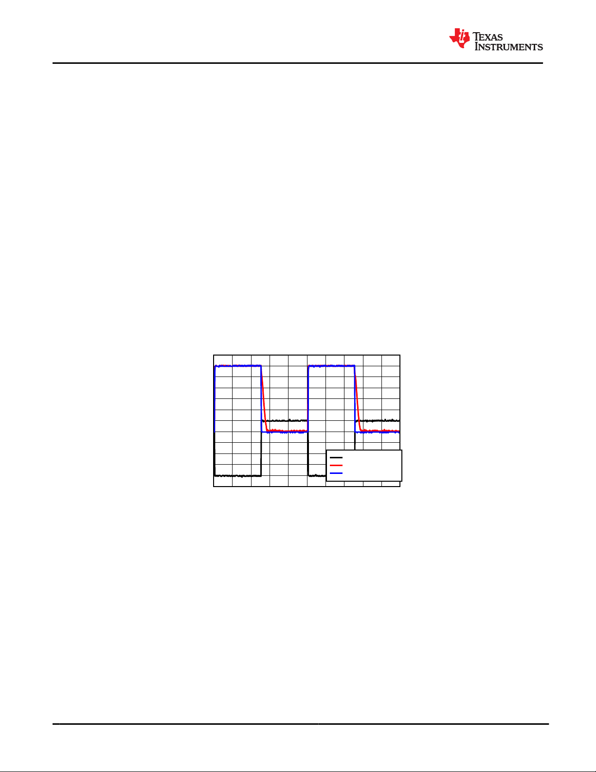
Time (s)
Voltage (V)
-0.001 -0.0006 -0.0002 0.0002 0.0006 0.001
-0.5
0
0.5
1
1.5
2
2.5
3
3.5
4
4.5
5
5.5
D001
Vin
Vka(Rsup=10k:)
Vka(Rsup=1k:)
TL431, TL432
SLVS543Q – AUGUST 2004 – REVISED JULY 2022
www.ti.com
10.2.1.2.2 Output Voltage and Logic Input Level
In order for TL431 to properly be used as a comparator, the logic output must be readable by the receiving logic
device. This is accomplished by knowing the input high and low level threshold voltage levels, typically denoted
by VIH & VIL.
As seen in Figure 10-2, TL431's output low level voltage in open-loop/comparator mode is ~2 V, which is
typically sufficient for 5V supplied logic. However, would not work for 3.3 V & 1.8 V supplied logic. In order to
accomodate this a resistive divider can be tied to the output to attenuate the output voltage to a voltage legible to
the receiving low voltage logic device.
TL431's output high voltage is equal to V
due to TL431 being open-collector. If V
SUP
is much higher than the
SUP
receiving logic's maximum input voltage tolerance, the output must be attenuated to accomadate the outgoing
logic's reliability.
When using a resistive divider on the output, be sure to make the sum of the resistive divider (R1 & R2 in Figure
10-1) is much greater than R
in order to not interfere with TL431's ability to pull close to V
SUP
when turning
SUP
off.
10.2.1.2.2.1 Input Resistance
TL431 requires an input resistance in this application in order to source the reference current (I
) needed from
REF
this device to be in the proper operating regions while turing on. The actual voltage seen at the ref pin will be
V
REF=VIN-IREF*RIN
will mitigate the error that I
. Since I
can be as high as 4 µA it is recommended to use a resistance small enough that
REF
creates from VIN.
REF
10.2.1.3 Application Curve
Figure 10-2. Output Response With Various Cathode Currents
24 Submit Document Feedback
Copyright © 2022 Texas Instruments Incorporated
Product Folder Links: TL431 TL432
Page 25
REF
CATHODE
ANODE
R2
V
SUP
R
SUP
R1
V
O
(
R1
V
ref
0.1%
R2
0.1%
TL431
= 1 + V
ref
)
C
L
www.ti.com
SLVS543Q – AUGUST 2004 – REVISED JULY 2022
10.2.2 Shunt Regulator/Reference
Figure 10-3. Shunt Regulator Schematic
10.2.2.1 Design Requirements
For this design example, use the parameters listed in Table 10-1 as the input parameters.
Table 10-2. Design Parameters
DESIGN PARAMETER EXAMPLE VALUE
Reference Initial Accuracy 1.0 %
Supply Voltage 24 V
Cathode Current (Ik) 5 mA
Output Voltage Level 2.5 V - 36 V
Load Capacitance 100 nF
Feedback Resistor Values and Accuracy (R1 & R2) 10 kΩ
TL431, TL432
10.2.2.2 Detailed Design Procedure
When using TL431 as a Shunt Regulator, determine the following:
• Input Voltage Range
• Temperature Range
• Total Accuracy
• Cathode Current
• Reference Initial Accuracy
• Output Capacitance
10.2.2.2.1 Programming Output/Cathode Voltage
In order to program the cathode voltage to a regulated voltage a resistive bridge must be shunted between
the cathode and anode pins with the mid point tied to the reference pin. This can be seen in Figure 10-3,
with R1 & R2 being the resistive bridge. The cathode/output voltage in the shunt regulator configuration can be
approximated by the equation shown in Figure 10-3. The cathode voltage can be more accuratel determined by
taking in to account the cathode current:
Vo=(1+R1/R2)*V
REF-IREF
*R1
In order for this equation to be valid, TL43xx must be fully biased so that it has enough open loop gain
to mitigate any gain error. This can be done by meeting the Imin spec denoted in Electrical Characteristics,
TL431C, TL432C.
Copyright © 2022 Texas Instruments Incorporated
Submit Document Feedback
25
Product Folder Links: TL431 TL432
Page 26

Time (s)
Voltage (V)
-5E-6 -3E-6 -1E-6 1E-6 3E-6 5E-6
-6
-3
0
3
6
9
12
15
18
21
24
27
D001
Vsup
Vka=Vref
R1=10k: & R2=10k:
R1=38k: & R2=10k:
TL431, TL432
SLVS543Q – AUGUST 2004 – REVISED JULY 2022
10.2.2.2.2 Total Accuracy
www.ti.com
When programming the output above unity gain (VKA=V
effect the overall accuracy beyond V
. These errors include:
REF
), TL43xx is susceptible to other errors that may
REF
• R1 and R2 accuracies
• V
• ΔV
- Change in reference voltage over temperature
I(dev)
/ ΔVKA - Change in reference voltage to the change in cathode voltage
REF
• |zKA| - Dynamic impedance, causing a change in cathode voltage with cathode current
Worst case cathode voltage can be determined taking all of the variables in to account. Application note Setting
the Shunt Voltage on an Adjustable Shunt Regulator (SLVA445) assists designers in setting the shunt voltage to
achieve optimum accuracy for this device.
10.2.2.2.3 Stability
Though TL43xx is stable with no capacitive load, the device that receives the shunt regulator's output voltage
could present a capacitive load that is within the TL43xx region of stability, shown inFigure 7-16 and Figure 7-18.
Also, designers may use capacitive loads to improve the transient response or for power supply decoupling.
When using additional capacitance between Cathode and Anode, refer to Figure 7-16 and Figure 7-18. Also,
application note Understanding Stability Boundary Conditions Charts in TL431, TL432 Data Sheet (SLVA482)
will provide a deeper understanding of this devices stability characteristics and aid the user in making the right
choices when choosing a load capacitor.
10.2.2.2.4 Start-Up Time
As shown in Figure 10-4, TL43xx has a fast response up to ~2 V and then slowly charges to it's programmed
value. This is due to the compensation capacitance (shown in Figure 9-2) the TL43xx has to meet it's stability
criteria. Despite the secondary delay, TL43xx still has a fast response suitable for many clamp applications.
10.2.2.3 Application Curve
26 Submit Document Feedback
Figure 10-4. TL43xx Start-Up Response
Copyright © 2022 Texas Instruments Incorporated
Product Folder Links: TL431 TL432
Page 27

R
(see Note A)
V
O
TL431
V
I(BATT)
2N222
2N222
4.7 kΩ
R1
0.1%
R2
0.1%
0.01 µF
30 Ω
O ref
R1
V = 1 + V
R2
æ ö
ç ÷
è ø
V
O
TL431
V
I(BATT)
uA7805
IN
OUT
Common
R1
R2
V
O
1
R1
R2
V
ref
Minimum V
O
V
ref
5 V
=
+
=
+
(
(
V
O
TL431
V
I(BATT)
R1
R2
V
O
1
R1
R2
V
ref
=
+
(
(
V
O
TL431
V
I(BATT)
R1
R2
C
(see Note A)
www.ti.com
10.3 System Examples
SLVS543Q – AUGUST 2004 – REVISED JULY 2022
TL431, TL432
A. R should provide cathode current ≥1 mA to the TL431 at minimum V
Figure 10-5. Precision High-Current Series Regulator
Figure 10-6. Output Control of a Three-Terminal Fixed Regulator
(BATT)
.
Figure 10-7. High-Current Shunt Regulator
A. Refer to the stability boundary conditions in Figure 7-16 and Figure 7-18 to determine allowable values for C.
Copyright © 2022 Texas Instruments Incorporated
Figure 10-8. Crowbar Circuit
Product Folder Links: TL431 TL432
Submit Document Feedback
27
Page 28

VO≈5 V, 1.5 A
TL431
V
I(BATT)
LM317
IN OUT
Adjust
243 Ω
0.1%
243 Ω
0.1%
8.2 kΩ
VO≈5 V
TL431
V
I(BATT)
27.4 kΩ
0.1%
R
b
(see Note A)
27.4 kΩ
0.1%
TL431
12 V
V
CC
5 V
6.8 kΩ
10 kΩ
10 kΩ
0.1%
10 kΩ
0.1%
X
Not
Used
Feedback
TL598
+
−
TL431, TL432
SLVS543Q – AUGUST 2004 – REVISED JULY 2022
Figure 10-9. Precision 5-V, 1.5-A Regulator
www.ti.com
A. Rb should provide cathode current ≥1 mA to the TL431.
Figure 10-10. Efficient 5-V Precision Regulator
Figure 10-11. PWM Converter With Reference
28 Submit Document Feedback
Copyright © 2022 Texas Instruments Incorporated
Product Folder Links: TL431 TL432
Page 29

TL431
V
I(BATT)
R3
(see Note A)
R1A
R4
(see Note A)
R2BR2A
R1B
Low Limit = 1 +
R1B
R2B
V
ref
High Li mi t = 1 +
R1A
R2A
V
ref
LED on When Low Limit < V
I(BATT)
< High Limit
TL431
650 Ω
2 kΩ
C
On
Off
R
12 V
n
ref
12 V
Delay = R × C × I
12 V – V
æ ö
ç ÷
ç ÷
è ø
TL431
I
O
R
CL
0.1%
R1
V
I(BATT)
I
out
V
ref
R
CL
I
KA
R1
V
I(BATT
)
I
O
h
FE
I
KA
+
+
=
=
TL431
R
S
0.1%
I
O
V
I(BATT)
I
O
V
ref
R
S
=
www.ti.com
SLVS543Q – AUGUST 2004 – REVISED JULY 2022
TL431, TL432
A. Select R3 and R4 to provide the desired LED intensity and cathode current ≥1 mA to the TL431 at the available V
Figure 10-12. Voltage Monitor
Figure 10-13. Delay Timer
I(BATT)
.
Copyright © 2022 Texas Instruments Incorporated
Figure 10-15. Precision Constant-Current Sink
Figure 10-14. Precision Current Limiter
Product Folder Links: TL431 TL432
Submit Document Feedback
29
Page 30

TL432 - DBZ
(TOP VIEW)
REF
1
CATHODE
2
3
ANODE
Rsup
Rref
Vsup
C
L
Vin
GND
GND
TL431, TL432
SLVS543Q – AUGUST 2004 – REVISED JULY 2022
www.ti.com
11 Power Supply Recommendations
When using TL43xx as a Linear Regulator to supply a load, designers will typically use a bypass capacitor on
the output/cathode pin. When doing this, be sure that the capacitance is within the stability criteria shown in
Figure 7-16 and Figure 7-18.
In order to not exceed the maximum cathode current, be sure that the supply voltage is current limited. Also, be
sure to limit the current being driven into the Ref pin, as not to exceed it's absolute maximum rating.
For applications shunting high currents, pay attention to the cathode and anode trace lengths, adjusting the
width of the traces to have the proper current density.
12 Layout
12.1 Layout Guidelines
Bypass capacitors should be placed as close to the part as possible. Current-carrying traces need to have
widths appropriate for the amount of current they are carrying; in the case of the TL43xx, these currents will be
low.
12.2 Layout Example
30 Submit Document Feedback
Figure 12-1. DBZ Layout Example
Copyright © 2022 Texas Instruments Incorporated
Product Folder Links: TL431 TL432
Page 31

TL431 X X XXX X XX
Product
Operating Free-Air
Temperature
Package
Type
Package
Quantity Eco Plan
Initial
Accuracy
1: TL431
2: TL432*
B: 0.5%
A: 1%
(Blank): 2%
LP: TO-92
LPM: TO-92
(Formed Lead)
DCK: SC-70
D: SOIC
P: PDIP
PK: SOT-89
PS: SO
DBV: SOT-23-5
DBZ: SOT-23-3
PW: TSSOP
C: 0°C to 70°C
I: -40°C to 85°C
Q: -40°C to 125°C
R: Tape & Reel
T: Small Tape & Reel
G3: Legacy Designator
G4: Legacy Designator
E3: Legacy Designator
E4: Legacy Designator
*(Cathode and REF
pins are switched)
www.ti.com
SLVS543Q – AUGUST 2004 – REVISED JULY 2022
TL431, TL432
13 Device and Documentation Support
13.1 Device Nomenclature
TI assigns suffixes and prefixes to differentiate all the combinations of the TL43x family. The Eco Plan designator
is a legacy designator that was used to differentiate Pb-free and Green devices. More details and possible
orderable combinations are located on the Package Option Addendum in Mechanical, Packaging, and Orderable
Information.
13.2 Related Links
The table below lists quick access links. Categories include technical documents, support and community
resources, tools and software, and quick access to sample or buy.
13.3 Receiving Notification of Documentation Updates
To receive notification of documentation updates, navigate to the device product folder on ti.com. Click on
Subscribe to updates to register and receive a weekly digest of any product information that has changed. For
change details, review the revision history included in any revised document.
13.4 Support Resources
TI E2E™ support forums are an engineer's go-to source for fast, verified answers and design help — straight
from the experts. Search existing answers or ask your own question to get the quick design help you need.
Linked content is provided "AS IS" by the respective contributors. They do not constitute TI specifications and do
not necessarily reflect TI's views; see TI's Terms of Use.
13.5 Trademarks
TI E2E™ is a trademark of Texas Instruments.
All trademarks are the property of their respective owners.
Copyright © 2022 Texas Instruments Incorporated
Table 13-1. Related Links
PARTS PRODUCT FOLDER SAMPLE & BUY
TL431 Click here Click here Click here Click here Click here
TL432 Click here Click here Click here Click here Click here
TECHNICAL
DOCUMENTS
TOOLS &
SOFTWARE
SUPPORT &
COMMUNITY
Product Folder Links: TL431 TL432
Submit Document Feedback
31
Page 32

TL431, TL432
SLVS543Q – AUGUST 2004 – REVISED JULY 2022
www.ti.com
13.6 Electrostatic Discharge Caution
This integrated circuit can be damaged by ESD. Texas Instruments recommends that all integrated circuits be handled
with appropriate precautions. Failure to observe proper handling and installation procedures can cause damage.
ESD damage can range from subtle performance degradation to complete device failure. Precision integrated circuits may
be more susceptible to damage because very small parametric changes could cause the device not to meet its published
specifications.
13.7 Glossary
TI Glossary This glossary lists and explains terms, acronyms, and definitions.
14 Mechanical, Packaging, and Orderable Information
The following pages include mechanical packaging and orderable information. This information is the most
current data available for the designated devices. This data is subject to change without notice and revision of
this document. For browser based versions of this data sheet, refer to the left hand navigation.
32 Submit Document Feedback
Copyright © 2022 Texas Instruments Incorporated
Product Folder Links: TL431 TL432
Page 33

PACKAGE OPTION ADDENDUM
www.ti.com
PACKAGING INFORMATION
Orderable Device Status
TL431ACD ACTIVE SOIC D 8 75 RoHS & Green NIPDAU Level-1-260C-UNLIM 0 to 70 431AC
TL431ACDBVR ACTIVE SOT-23 DBV 5 3000 RoHS & Green NIPDAU | SN Level-1-260C-UNLIM 0 to 70 (TACG, TACJ, TACS)
TL431ACDBVRE4 ACTIVE SOT-23 DBV 5 3000 RoHS & Green NIPDAU Level-1-260C-UNLIM 0 to 70 TACG
TL431ACDBVRG4 ACTIVE SOT-23 DBV 5 3000 RoHS & Green NIPDAU Level-1-260C-UNLIM 0 to 70 TACG
TL431ACDBVT ACTIVE SOT-23 DBV 5 250 RoHS & Green NIPDAU | SN Level-1-260C-UNLIM 0 to 70 (TACG, TACJ, TACU)
TL431ACDBZR ACTIVE SOT-23 DBZ 3 3000 RoHS & Green NIPDAU | SN
TL431ACDBZRG4 ACTIVE SOT-23 DBZ 3 3000 RoHS & Green NIPDAU Level-1-260C-UNLIM 0 to 70 TAC3
TL431ACDBZT ACTIVE SOT-23 DBZ 3 250 RoHS & Green NIPDAU | SN Level-1-260C-UNLIM 0 to 70 (TAC3, TACG, TACS,
TL431ACDBZTG4 ACTIVE SOT-23 DBZ 3 250 RoHS & Green NIPDAU Level-1-260C-UNLIM 0 to 70 TAC3
TL431ACDCKR ACTIVE SC70 DCK 6 3000 RoHS & Green NIPDAU Level-1-260C-UNLIM 0 to 70 (T4S, T4U)
TL431ACDG4 ACTIVE SOIC D 8 75 RoHS & Green NIPDAU Level-1-260C-UNLIM 0 to 70 431AC
TL431ACDR ACTIVE SOIC D 8 2500 RoHS & Green NIPDAU | SN Level-1-260C-UNLIM 0 to 70 431AC
TL431ACDRE4 ACTIVE SOIC D 8 2500 RoHS & Green NIPDAU Level-1-260C-UNLIM 0 to 70 431AC
TL431ACDRG4 ACTIVE SOIC D 8 2500 RoHS & Green NIPDAU Level-1-260C-UNLIM 0 to 70 431AC
TL431ACLP ACTIVE TO-92 LP 3 1000 RoHS & Green SN N / A for Pkg Type 0 to 70 TL431AC
TL431ACLPE3 ACTIVE TO-92 LP 3 1000 RoHS & Green SN N / A for Pkg Type 0 to 70 TL431AC
TL431ACLPM ACTIVE TO-92 LP 3 2000 RoHS & Green SN N / A for Pkg Type 0 to 70 TL431AC
TL431ACLPME3 ACTIVE TO-92 LP 3 2000 RoHS & Green SN N / A for Pkg Type 0 to 70 TL431AC
TL431ACLPR ACTIVE TO-92 LP 3 2000 RoHS & Green SN N / A for Pkg Type 0 to 70 TL431AC
Package Type Package
(1)
Drawing
Pins Package
Qty
Eco Plan
(2)
Lead finish/
Ball material
(6)
| NIPDAUAG
MSL Peak Temp
(3)
Op Temp (°C) Device Marking
Level-1-260C-UNLIM 0 to 70 (TAC3, TACG, TACS,
TACU)
TACU)
18-Aug-2022
Samples
(4/5)
Samples
Samples
Samples
Samples
Samples
Samples
Samples
Samples
Samples
Samples
Samples
Samples
Samples
Samples
Samples
Samples
Samples
Samples
Samples
Addendum-Page 1
Page 34

PACKAGE OPTION ADDENDUM
www.ti.com
Orderable Device Status
Package Type Package
(1)
Drawing
Pins Package
Qty
Eco Plan
(2)
Lead finish/
Ball material
(6)
MSL Peak Temp
(3)
Op Temp (°C) Device Marking
TL431ACLPRE3 ACTIVE TO-92 LP 3 2000 RoHS & Green SN N / A for Pkg Type 0 to 70 TL431AC
TL431ACP ACTIVE PDIP P 8 50 RoHS & Green NIPDAU N / A for Pkg Type 0 to 70 TL431ACP
TL431ACPK ACTIVE SOT-89 PK 3 1000 RoHS & Green SN Level-2-260C-1 YEAR 0 to 70 4A
TL431ACPKG3 ACTIVE SOT-89 PK 3 1000 RoHS & Green SN Level-2-260C-1 YEAR 0 to 70 4A
TL431ACPSR ACTIVE SO PS 8 2000 RoHS & Green NIPDAU Level-1-260C-UNLIM 0 to 70 T431A
TL431ACPW ACTIVE TSSOP PW 8 150 RoHS & Green NIPDAU Level-1-260C-UNLIM 0 to 70 T431A
TL431ACPWR ACTIVE TSSOP PW 8 2000 RoHS & Green NIPDAU Level-1-260C-UNLIM 0 to 70 T431A
TL431AID ACTIVE SOIC D 8 75 RoHS & Green NIPDAU Level-1-260C-UNLIM -40 to 85 431AI
TL431AIDBVR ACTIVE SOT-23 DBV 5 3000 RoHS & Green NIPDAU | SN Level-1-260C-UNLIM -40 to 85 (TAIG, TAIJ, TAIS)
TL431AIDBVRE4 ACTIVE SOT-23 DBV 5 3000 RoHS & Green NIPDAU Level-1-260C-UNLIM -40 to 85 TAIG
TL431AIDBVRG4 ACTIVE SOT-23 DBV 5 3000 RoHS & Green NIPDAU Level-1-260C-UNLIM -40 to 85 TAIG
TL431AIDBVT ACTIVE SOT-23 DBV 5 250 RoHS & Green NIPDAU | SN Level-1-260C-UNLIM -40 to 85 (TAIG, TAIJ, TAIU)
TL431AIDBVTG4 ACTIVE SOT-23 DBV 5 250 RoHS & Green NIPDAU Level-1-260C-UNLIM -40 to 85 TAIG
TL431AIDBZR ACTIVE SOT-23 DBZ 3 3000 RoHS & Green NIPDAU | SN Level-1-260C-UNLIM -40 to 85 (T3AG, TAI3, TAIS,
TL431AIDBZRG4 ACTIVE SOT-23 DBZ 3 3000 RoHS & Green NIPDAU Level-1-260C-UNLIM -40 to 85 TAI3
TL431AIDBZT ACTIVE SOT-23 DBZ 3 250 RoHS & Green NIPDAU | SN Level-1-260C-UNLIM -40 to 85 (T3AG, TAI3, TAIS,
TL431AIDBZTG4 ACTIVE SOT-23 DBZ 3 250 RoHS & Green NIPDAU Level-1-260C-UNLIM -40 to 85 TAI3
TL431AIDCKR ACTIVE SC70 DCK 6 3000 RoHS & Green NIPDAU Level-1-260C-UNLIM -40 to 85 T5U
TL431AIDCKRE4 ACTIVE SC70 DCK 6 3000 RoHS & Green NIPDAU Level-1-260C-UNLIM -40 to 85 T5U
TL431AIDCKT ACTIVE SC70 DCK 6 250 RoHS & Green NIPDAU Level-1-260C-UNLIM -40 to 85 T5U
TAIU)
TAIU)
18-Aug-2022
Samples
(4/5)
Samples
Samples
Samples
Samples
Samples
Samples
Samples
Samples
Samples
Samples
Samples
Samples
Samples
Samples
Samples
Samples
Samples
Samples
Samples
Samples
Addendum-Page 2
Page 35

PACKAGE OPTION ADDENDUM
www.ti.com
Orderable Device Status
Package Type Package
(1)
Drawing
Pins Package
Qty
Eco Plan
(2)
Lead finish/
Ball material
(6)
MSL Peak Temp
(3)
Op Temp (°C) Device Marking
TL431AIDG4 ACTIVE SOIC D 8 75 RoHS & Green NIPDAU Level-1-260C-UNLIM -40 to 85 431AI
TL431AIDR ACTIVE SOIC D 8 2500 RoHS & Green NIPDAU | SN Level-1-260C-UNLIM -40 to 85 431AI
TL431AIDRG4 ACTIVE SOIC D 8 2500 RoHS & Green NIPDAU Level-1-260C-UNLIM -40 to 85 431AI
TL431AILP ACTIVE TO-92 LP 3 1000 RoHS & Green SN N / A for Pkg Type -40 to 85 TL431AI
TL431AILPE3 ACTIVE TO-92 LP 3 1000 RoHS & Green SN N / A for Pkg Type -40 to 85 TL431AI
TL431AILPM ACTIVE TO-92 LP 3 2000 RoHS & Green SN N / A for Pkg Type -40 to 85 TL431AI
TL431AILPME3 ACTIVE TO-92 LP 3 2000 RoHS & Green SN N / A for Pkg Type -40 to 85 TL431AI
TL431AILPR ACTIVE TO-92 LP 3 2000 RoHS & Green SN N / A for Pkg Type -40 to 85 TL431AI
TL431AILPRE3 ACTIVE TO-92 LP 3 2000 RoHS & Green SN N / A for Pkg Type -40 to 85 TL431AI
TL431AIP ACTIVE PDIP P 8 50 RoHS & Green NIPDAU N / A for Pkg Type -40 to 85 TL431AIP
TL431AIPE4 ACTIVE PDIP P 8 50 RoHS & Green NIPDAU N / A for Pkg Type -40 to 85 TL431AIP
TL431AIPK ACTIVE SOT-89 PK 3 1000 RoHS & Green SN Level-2-260C-1 YEAR -40 to 85 4B
TL431AIPKG3 ACTIVE SOT-89 PK 3 1000 RoHS & Green SN Level-2-260C-1 YEAR -40 to 85 4B
TL431AQDBVR ACTIVE SOT-23 DBV 5 3000 RoHS & Green NIPDAU | SN Level-1-260C-UNLIM -40 to 125 (TAQG, TAQJ, TAQU)
TL431AQDBVT ACTIVE SOT-23 DBV 5 250 RoHS & Green NIPDAU | SN Level-1-260C-UNLIM -40 to 125 (TAQG, TAQJ, TAQU)
TL431AQDBZR ACTIVE SOT-23 DBZ 3 3000 RoHS & Green NIPDAUAG | SN Level-1-260C-UNLIM -40 to 125 (TAQ3, TAQG, TAQS,
TL431AQDBZRG4 ACTIVE SOT-23 DBZ 3 3000 RoHS & Green NIPDAUAG Level-1-260C-UNLIM -40 to 125 TAQS
TL431AQDBZT ACTIVE SOT-23 DBZ 3 250 RoHS & Green NIPDAUAG | SN Level-1-260C-UNLIM -40 to 125 (TAQG, TAQS, TAQU)
TL431AQDBZTG4 ACTIVE SOT-23 DBZ 3 250 RoHS & Green NIPDAUAG Level-1-260C-UNLIM -40 to 125 TAQS
TL431AQDCKR ACTIVE SC70 DCK 6 3000 RoHS & Green NIPDAU Level-1-260C-UNLIM -40 to 125 T7U
TAQU)
18-Aug-2022
Samples
(4/5)
Samples
Samples
Samples
Samples
Samples
Samples
Samples
Samples
Samples
Samples
Samples
Samples
Samples
Samples
Samples
Samples
Samples
Samples
Samples
Samples
Addendum-Page 3
Page 36

PACKAGE OPTION ADDENDUM
www.ti.com
Orderable Device Status
Package Type Package
(1)
Drawing
Pins Package
Qty
Eco Plan
(2)
Lead finish/
Ball material
(6)
MSL Peak Temp
(3)
Op Temp (°C) Device Marking
TL431AQDCKT ACTIVE SC70 DCK 6 250 RoHS & Green NIPDAU Level-1-260C-UNLIM -40 to 125 T7U
TL431AQPK ACTIVE SOT-89 PK 3 1000 RoHS & Green SN Level-2-260C-1 YEAR -40 to 125 4D
TL431AQPKG3 ACTIVE SOT-89 PK 3 1000 RoHS & Green SN Level-2-260C-1 YEAR -40 to 125 4D
TL431BCD ACTIVE SOIC D 8 75 RoHS & Green NIPDAU Level-1-260C-UNLIM 0 to 70 T431B
TL431BCDBVR ACTIVE SOT-23 DBV 5 3000 RoHS & Green NIPDAU | SN Level-1-260C-UNLIM 0 to 70 (T3GG, T3GJ, T3GU)
TL431BCDBVT ACTIVE SOT-23 DBV 5 250 RoHS & Green NIPDAU | SN Level-1-260C-UNLIM 0 to 70 (T3GG, T3GJ, T3GU)
TL431BCDBVTG4 ACTIVE SOT-23 DBV 5 250 RoHS & Green NIPDAU Level-1-260C-UNLIM 0 to 70 T3GG
TL431BCDBZR ACTIVE SOT-23 DBZ 3 3000 RoHS & Green NIPDAU | SN Level-1-260C-UNLIM 0 to 70 (T3G3, T3GG, T3GS,
TL431BCDBZRG4 ACTIVE SOT-23 DBZ 3 3000 RoHS & Green NIPDAU Level-1-260C-UNLIM 0 to 70 T3G3
TL431BCDBZT ACTIVE SOT-23 DBZ 3 250 RoHS & Green NIPDAU | SN Level-1-260C-UNLIM 0 to 70 (T3G3, T3GG, T3GS,
TL431BCDBZTG4 ACTIVE SOT-23 DBZ 3 250 RoHS & Green NIPDAU Level-1-260C-UNLIM 0 to 70 T3G3
TL431BCDCKR ACTIVE SC70 DCK 6 3000 RoHS & Green NIPDAU Level-1-260C-UNLIM 0 to 70 T2U
TL431BCDCKT ACTIVE SC70 DCK 6 250 RoHS & Green NIPDAU Level-1-260C-UNLIM 0 to 70 T2U
TL431BCDE4 ACTIVE SOIC D 8 75 RoHS & Green NIPDAU Level-1-260C-UNLIM 0 to 70 T431B
TL431BCDR ACTIVE SOIC D 8 2500 RoHS & Green NIPDAU Level-1-260C-UNLIM 0 to 70 T431B
TL431BCDRG4 ACTIVE SOIC D 8 2500 TBD Call TI Call TI 0 to 70
TL431BCLP ACTIVE TO-92 LP 3 1000 RoHS & Green SN N / A for Pkg Type 0 to 70 T431B
TL431BCLPE3 ACTIVE TO-92 LP 3 1000 RoHS & Green SN N / A for Pkg Type 0 to 70 T431B
TL431BCLPR ACTIVE TO-92 LP 3 2000 RoHS & Green SN N / A for Pkg Type 0 to 70 T431B
TL431BCP ACTIVE PDIP P 8 50 RoHS & Green NIPDAU N / A for Pkg Type 0 to 70 TL431BCP
T3GU)
T3GU)
18-Aug-2022
Samples
(4/5)
Samples
Samples
Samples
Samples
Samples
Samples
Samples
Samples
Samples
Samples
Samples
Samples
Samples
Samples
Samples
Samples
Samples
Samples
Samples
Samples
Addendum-Page 4
Page 37

PACKAGE OPTION ADDENDUM
www.ti.com
Orderable Device Status
Package Type Package
(1)
Drawing
Pins Package
Qty
Eco Plan
(2)
Lead finish/
Ball material
(6)
MSL Peak Temp
(3)
Op Temp (°C) Device Marking
TL431BCPK ACTIVE SOT-89 PK 3 1000 RoHS & Green SN Level-2-260C-1 YEAR 0 to 70 4C
TL431BCPKG3 ACTIVE SOT-89 PK 3 1000 RoHS & Green SN Level-2-260C-1 YEAR 0 to 70 4C
TL431BCPSR ACTIVE SO PS 8 2000 RoHS & Green NIPDAU Level-1-260C-UNLIM 0 to 70 T431B
TL431BCPWR ACTIVE TSSOP PW 8 2000 RoHS & Green NIPDAU Level-1-260C-UNLIM 0 to 70 T431B
TL431BID ACTIVE SOIC D 8 75 RoHS & Green NIPDAU Level-1-260C-UNLIM -40 to 85 Z431B
TL431BIDBVR ACTIVE SOT-23 DBV 5 3000 RoHS & Green NIPDAU | SN Level-1-260C-UNLIM -40 to 85 (T3FG, T3FJ, T3FU)
TL431BIDBVT ACTIVE SOT-23 DBV 5 250 RoHS & Green NIPDAU | SN Level-1-260C-UNLIM -40 to 85 (T3FG, T3FJ, T3FU)
TL431BIDBVTG4 ACTIVE SOT-23 DBV 5 250 RoHS & Green NIPDAU Level-1-260C-UNLIM -40 to 85 T3FG
TL431BIDBZR ACTIVE SOT-23 DBZ 3 3000 RoHS & Green NIPDAU | SN Level-1-260C-UNLIM -40 to 85 (T3F3, T3FG, T3FS,
TL431BIDBZRG4 ACTIVE SOT-23 DBZ 3 3000 RoHS & Green NIPDAU Level-1-260C-UNLIM -40 to 85 T3F3
TL431BIDBZT ACTIVE SOT-23 DBZ 3 250 RoHS & Green NIPDAU | SN
Level-1-260C-UNLIM -40 to 85 (T3F3, T3FG, T3FS,
| NIPDAUAG
TL431BIDBZTG4 ACTIVE SOT-23 DBZ 3 250 RoHS & Green NIPDAU Level-1-260C-UNLIM -40 to 85 T3F3
TL431BIDCKR ACTIVE SC70 DCK 6 3000 RoHS & Green NIPDAU Level-1-260C-UNLIM -40 to 85 T3U
TL431BIDCKT ACTIVE SC70 DCK 6 250 RoHS & Green NIPDAU Level-1-260C-UNLIM -40 to 85 T3U
TL431BIDE4 ACTIVE SOIC D 8 75 RoHS & Green NIPDAU Level-1-260C-UNLIM -40 to 85 Z431B
TL431BIDG4 ACTIVE SOIC D 8 75 RoHS & Green NIPDAU Level-1-260C-UNLIM -40 to 85 Z431B
TL431BIDR ACTIVE SOIC D 8 2500 RoHS & Green NIPDAU | SN Level-1-260C-UNLIM -40 to 85 Z431B
TL431BIDRE4 ACTIVE SOIC D 8 2500 RoHS & Green NIPDAU Level-1-260C-UNLIM -40 to 85 Z431B
TL431BIDRG4 ACTIVE SOIC D 8 2500 RoHS & Green NIPDAU Level-1-260C-UNLIM -40 to 85 Z431B
TL431BILP ACTIVE TO-92 LP 3 1000 RoHS & Green SN N / A for Pkg Type -40 to 85 Z431B
T3FU)
T3FU)
18-Aug-2022
Samples
(4/5)
Samples
Samples
Samples
Samples
Samples
Samples
Samples
Samples
Samples
Samples
Samples
Samples
Samples
Samples
Samples
Samples
Samples
Samples
Samples
Samples
Addendum-Page 5
Page 38

PACKAGE OPTION ADDENDUM
www.ti.com
Orderable Device Status
Package Type Package
(1)
Drawing
Pins Package
Qty
Eco Plan
(2)
Lead finish/
Ball material
(6)
MSL Peak Temp
(3)
Op Temp (°C) Device Marking
TL431BILPE3 ACTIVE TO-92 LP 3 1000 RoHS & Green SN N / A for Pkg Type -40 to 85 Z431B
TL431BILPR ACTIVE TO-92 LP 3 2000 RoHS & Green SN N / A for Pkg Type -40 to 85 Z431B
TL431BILPRE3 ACTIVE TO-92 LP 3 2000 RoHS & Green SN N / A for Pkg Type -40 to 85 Z431B
TL431BIP ACTIVE PDIP P 8 50 RoHS & Green NIPDAU N / A for Pkg Type -40 to 85 TL431BIP
TL431BIPK ACTIVE SOT-89 PK 3 1000 RoHS & Green SN Level-2-260C-1 YEAR -40 to 85 4I
TL431BIPKG3 ACTIVE SOT-89 PK 3 1000 RoHS & Green SN Level-2-260C-1 YEAR -40 to 85 4I
TL431BQD ACTIVE SOIC D 8 75 RoHS & Green NIPDAU Level-1-260C-UNLIM -40 to 125 T431BQ
TL431BQDBVR ACTIVE SOT-23 DBV 5 3000 RoHS & Green NIPDAU | SN Level-1-260C-UNLIM -40 to 125 (T3HJ, T3HU)
TL431BQDBVRG4 ACTIVE SOT-23 DBV 5 3000 RoHS & Green NIPDAU Level-1-260C-UNLIM -40 to 125 (T3HJ, T3HU)
TL431BQDBVT ACTIVE SOT-23 DBV 5 250 RoHS & Green NIPDAU | SN Level-1-260C-UNLIM -40 to 125 (T3HJ, T3HU)
TL431BQDBZR ACTIVE SOT-23 DBZ 3 3000 RoHS & Green NIPDAU | SN
Level-1-260C-UNLIM -40 to 125 (T3H3, T3HG, T3HS,
| NIPDAUAG
TL431BQDBZRG4 ACTIVE SOT-23 DBZ 3 3000 RoHS & Green NIPDAUAG Level-1-260C-UNLIM -40 to 125 T3HS
TL431BQDBZT ACTIVE SOT-23 DBZ 3 250 RoHS & Green NIPDAUAG | SN Level-1-260C-UNLIM -40 to 125 (T3HG, T3HS, T3HU)
TL431BQDBZTG4 ACTIVE SOT-23 DBZ 3 250 RoHS & Green NIPDAUAG Level-1-260C-UNLIM -40 to 125 T3HS
TL431BQDCKR ACTIVE SC70 DCK 6 3000 RoHS & Green NIPDAU Level-1-260C-UNLIM -40 to 125 T8U
TL431BQDCKT ACTIVE SC70 DCK 6 250 RoHS & Green NIPDAU Level-1-260C-UNLIM -40 to 125 T8U
TL431BQDE4 ACTIVE SOIC D 8 75 RoHS & Green NIPDAU Level-1-260C-UNLIM -40 to 125 T431BQ
TL431BQDR ACTIVE SOIC D 8 2500 RoHS & Green NIPDAU Level-1-260C-UNLIM -40 to 125 T431BQ
TL431BQDRG4 ACTIVE SOIC D 8 2500 RoHS & Green NIPDAU Level-1-260C-UNLIM -40 to 125 T431BQ
TL431BQLP ACTIVE TO-92 LP 3 1000 RoHS & Green SN N / A for Pkg Type -40 to 125 T431BQ
TL431BQLPM ACTIVE TO-92 LP 3 2000 RoHS & Green SN N / A for Pkg Type -40 to 125 T431BQ
T3HU)
18-Aug-2022
Samples
(4/5)
Samples
Samples
Samples
Samples
Samples
Samples
Samples
Samples
Samples
Samples
Samples
Samples
Samples
Samples
Samples
Samples
Samples
Samples
Samples
Samples
Samples
Addendum-Page 6
Page 39

PACKAGE OPTION ADDENDUM
www.ti.com
Orderable Device Status
TL431BQLPME3 ACTIVE TO-92 LP 3 2000 RoHS & Green SN N / A for Pkg Type -40 to 125 T431BQ
TL431BQLPR ACTIVE TO-92 LP 3 2000 RoHS & Green SN N / A for Pkg Type -40 to 125 T431BQ
TL431BQLPRE3 ACTIVE TO-92 LP 3 2000 RoHS & Green SN N / A for Pkg Type -40 to 125 T431BQ
TL431BQPK ACTIVE SOT-89 PK 3 1000 RoHS & Green SN Level-2-260C-1 YEAR -40 to 125 3H
TL431BQPKG3 ACTIVE SOT-89 PK 3 1000 RoHS & Green SN Level-2-260C-1 YEAR -40 to 125 3H
TL431CD ACTIVE SOIC D 8 75 RoHS & Green NIPDAU Level-1-260C-UNLIM 0 to 70 TL431C
TL431CDBVR ACTIVE SOT-23 DBV 5 3000 RoHS & Green NIPDAU | SN Level-1-260C-UNLIM 0 to 70 (T3CG, T3CJ, T3CS)
TL431CDBVT ACTIVE SOT-23 DBV 5 250 RoHS & Green NIPDAU | SN Level-1-260C-UNLIM 0 to 70 (T3CG, T3CJ, T3CS)
TL431CDBVTG4 ACTIVE SOT-23 DBV 5 250 RoHS & Green NIPDAU Level-1-260C-UNLIM 0 to 70 T3CG
TL431CDBZR ACTIVE SOT-23 DBZ 3 3000 RoHS & Green NIPDAU | SN Level-1-260C-UNLIM 0 to 70 (T3C3, T3CG, T3CS,
TL431CDBZRG4 ACTIVE SOT-23 DBZ 3 3000 RoHS & Green NIPDAU Level-1-260C-UNLIM 0 to 70 T3C3
TL431CDBZT ACTIVE SOT-23 DBZ 3 250 RoHS & Green NIPDAUAG | SN Level-1-260C-UNLIM 0 to 70 (T3CG, T3CS, T3CU)
TL431CDBZTG4 ACTIVE SOT-23 DBZ 3 250 RoHS & Green NIPDAUAG Level-1-260C-UNLIM 0 to 70 T3CS
TL431CDE4 ACTIVE SOIC D 8 75 RoHS & Green NIPDAU Level-1-260C-UNLIM 0 to 70 TL431C
TL431CDG4 ACTIVE SOIC D 8 75 RoHS & Green NIPDAU Level-1-260C-UNLIM 0 to 70 TL431C
TL431CDR ACTIVE SOIC D 8 2500 RoHS & Green NIPDAU | SN Level-1-260C-UNLIM 0 to 70 TL431C
TL431CDRG4 ACTIVE SOIC D 8 2500 RoHS & Green NIPDAU Level-1-260C-UNLIM 0 to 70 TL431C
TL431CLP ACTIVE TO-92 LP 3 1000 RoHS & Green SN N / A for Pkg Type 0 to 70 TL431C
TL431CLPE3 ACTIVE TO-92 LP 3 1000 RoHS & Green SN N / A for Pkg Type 0 to 70 TL431C
TL431CLPM ACTIVE TO-92 LP 3 2000 RoHS & Green SN N / A for Pkg Type 0 to 70 TL431C
Package Type Package
(1)
Drawing
Pins Package
Qty
Eco Plan
(2)
Lead finish/
Ball material
(6)
MSL Peak Temp
(3)
18-Aug-2022
Op Temp (°C) Device Marking
(4/5)
T3CU)
Samples
Samples
Samples
Samples
Samples
Samples
Samples
Samples
Samples
Samples
Samples
Samples
Samples
Samples
Samples
Samples
Samples
Samples
Samples
Samples
Samples
Addendum-Page 7
Page 40

PACKAGE OPTION ADDENDUM
www.ti.com
Orderable Device Status
TL431CLPME3 ACTIVE TO-92 LP 3 2000 RoHS & Green SN N / A for Pkg Type 0 to 70 TL431C
TL431CLPR ACTIVE TO-92 LP 3 2000 RoHS & Green SN N / A for Pkg Type 0 to 70 TL431C
TL431CLPRE3 ACTIVE TO-92 LP 3 2000 RoHS & Green SN N / A for Pkg Type 0 to 70 TL431C
TL431CP ACTIVE PDIP P 8 50 RoHS & Green NIPDAU N / A for Pkg Type 0 to 70 TL431CP
TL431CPE4 ACTIVE PDIP P 8 50 RoHS & Green NIPDAU N / A for Pkg Type 0 to 70 TL431CP
TL431CPK ACTIVE SOT-89 PK 3 1000 RoHS & Green SN Level-2-260C-1 YEAR 0 to 70 43
TL431CPKE6 ACTIVE SOT-89 PK 3 1000 RoHS &
TL431CPKG3 ACTIVE SOT-89 PK 3 1000 RoHS & Green SN Level-2-260C-1 YEAR 0 to 70 43
TL431CPSR ACTIVE SO PS 8 2000 RoHS & Green NIPDAU Level-1-260C-UNLIM 0 to 70 T431
TL431CPSRG4 ACTIVE SO PS 8 2000 RoHS & Green NIPDAU Level-1-260C-UNLIM 0 to 70 T431
TL431CPWR ACTIVE TSSOP PW 8 2000 RoHS & Green NIPDAU Level-1-260C-UNLIM 0 to 70 T431
TL431ID ACTIVE SOIC D 8 75 RoHS & Green NIPDAU Level-1-260C-UNLIM -40 to 85 TL431I
TL431IDBVR ACTIVE SOT-23 DBV 5 3000 RoHS & Green NIPDAU | SN Level-1-260C-UNLIM -40 to 85 (T3IG, T3IJ, T3IS)
TL431IDBVRE4 ACTIVE SOT-23 DBV 5 3000 RoHS & Green NIPDAU Level-1-260C-UNLIM -40 to 85 T3IG
TL431IDBVRG4 ACTIVE SOT-23 DBV 5 3000 RoHS & Green NIPDAU Level-1-260C-UNLIM -40 to 85 T3IG
TL431IDBVT ACTIVE SOT-23 DBV 5 250 RoHS & Green NIPDAU | SN Level-1-260C-UNLIM -40 to 85 (T3IG, T3IJ, T3IU)
TL431IDBZR ACTIVE SOT-23 DBZ 3 3000 RoHS & Green NIPDAUAG | SN Level-1-260C-UNLIM -40 to 85 (T3I3, T3IG, T3IS,
TL431IDBZRG4 ACTIVE SOT-23 DBZ 3 3000 RoHS & Green NIPDAUAG Level-1-260C-UNLIM -40 to 85 T3IS
TL431IDBZT ACTIVE SOT-23 DBZ 3 250 RoHS & Green NIPDAUAG | SN Level-1-260C-UNLIM -40 to 85 (T3IG, T3IS, T3IU)
TL431IDBZTG4 ACTIVE SOT-23 DBZ 3 250 RoHS & Green NIPDAUAG Level-1-260C-UNLIM -40 to 85 T3IS
Package Type Package
(1)
Drawing
Pins Package
Qty
Eco Plan
(2)
Non-Green
Lead finish/
Ball material
(6)
MSL Peak Temp
(3)
Op Temp (°C) Device Marking
SNBI Level-1-260C-UNLIM 0 to 70 43
T3IU)
18-Aug-2022
Samples
(4/5)
Samples
Samples
Samples
Samples
Samples
Samples
Samples
Samples
Samples
Samples
Samples
Samples
Samples
Samples
Samples
Samples
Samples
Samples
Samples
Samples
Addendum-Page 8
Page 41

PACKAGE OPTION ADDENDUM
www.ti.com
Orderable Device Status
Package Type Package
(1)
Drawing
Pins Package
Qty
Eco Plan
(2)
Lead finish/
Ball material
(6)
MSL Peak Temp
(3)
Op Temp (°C) Device Marking
TL431IDG4 ACTIVE SOIC D 8 75 RoHS & Green NIPDAU Level-1-260C-UNLIM -40 to 85 TL431I
TL431IDR ACTIVE SOIC D 8 2500 RoHS & Green NIPDAU | SN Level-1-260C-UNLIM -40 to 85 TL431I
TL431IDRE4 ACTIVE SOIC D 8 2500 TBD Call TI Call TI -40 to 85
TL431IDRG4 ACTIVE SOIC D 8 2500 RoHS & Green NIPDAU Level-1-260C-UNLIM -40 to 85 TL431I
TL431ILP ACTIVE TO-92 LP 3 1000 RoHS & Green SN N / A for Pkg Type -40 to 85 TL431I
TL431ILPE3 ACTIVE TO-92 LP 3 1000 RoHS & Green SN N / A for Pkg Type -40 to 85 TL431I
TL431ILPR ACTIVE TO-92 LP 3 2000 RoHS & Green SN N / A for Pkg Type -40 to 85 TL431I
TL431ILPRE3 ACTIVE TO-92 LP 3 2000 RoHS & Green SN N / A for Pkg Type -40 to 85 TL431I
TL431IP ACTIVE PDIP P 8 50 RoHS & Green NIPDAU N / A for Pkg Type -40 to 85 TL431IP
TL431IPE4 ACTIVE PDIP P 8 50 RoHS & Green NIPDAU N / A for Pkg Type -40 to 85 TL431IP
TL431IPK ACTIVE SOT-89 PK 3 1000 RoHS & Green SN Level-2-260C-1 YEAR -40 to 85 3I
TL431IPKG3 ACTIVE SOT-89 PK 3 1000 RoHS & Green SN Level-2-260C-1 YEAR -40 to 85 3I
TL431QD ACTIVE SOIC D 8 75 RoHS & Green NIPDAU Level-1-260C-UNLIM -40 to 125 T431Q
TL431QDBVR ACTIVE SOT-23 DBV 5 3000 RoHS & Green NIPDAU | SN Level-1-260C-UNLIM -40 to 125 (T3QG, T3QJ, T3QU)
TL431QDBVRG4 ACTIVE SOT-23 DBV 5 3000 RoHS & Green NIPDAU Level-1-260C-UNLIM -40 to 125 T3QG
TL431QDBVT ACTIVE SOT-23 DBV 5 250 RoHS & Green NIPDAU | SN Level-1-260C-UNLIM -40 to 125 (T3QG, T3QJ, T3QU)
TL431QDBZR ACTIVE SOT-23 DBZ 3 3000 RoHS & Green NIPDAUAG | SN Level-1-260C-UNLIM -40 to 125 (T3Q3, T3QG, T3QS,
TL431QDBZRG4 ACTIVE SOT-23 DBZ 3 3000 RoHS & Green NIPDAUAG Level-1-260C-UNLIM -40 to 125 T3QS
TL431QDBZT ACTIVE SOT-23 DBZ 3 250 RoHS & Green NIPDAUAG | SN Level-1-260C-UNLIM -40 to 125 (T3QG, T3QS, T3QU)
TL431QDBZTG4 ACTIVE SOT-23 DBZ 3 250 RoHS & Green NIPDAUAG Level-1-260C-UNLIM -40 to 125 T3QS
T3QU)
18-Aug-2022
Samples
(4/5)
Samples
Samples
Samples
Samples
Samples
Samples
Samples
Samples
Samples
Samples
Samples
Samples
Samples
Samples
Samples
Samples
Samples
Samples
Samples
Samples
Addendum-Page 9
Page 42

PACKAGE OPTION ADDENDUM
www.ti.com
Orderable Device Status
Package Type Package
(1)
Drawing
Pins Package
Qty
Eco Plan
(2)
Lead finish/
Ball material
(6)
MSL Peak Temp
(3)
Op Temp (°C) Device Marking
TL431QDCKR ACTIVE SC70 DCK 6 3000 RoHS & Green NIPDAU Level-1-260C-UNLIM -40 to 125 T6U
TL431QDCKT ACTIVE SC70 DCK 6 250 RoHS & Green NIPDAU Level-1-260C-UNLIM -40 to 125 T6U
TL431QDR ACTIVE SOIC D 8 2500 RoHS & Green NIPDAU Level-1-260C-UNLIM -40 to 125 T431Q
TL431QPK ACTIVE SOT-89 PK 3 1000 RoHS & Green SN Level-2-260C-1 YEAR -40 to 125 3Q
TL431QPKG3 ACTIVE SOT-89 PK 3 1000 RoHS & Green SN Level-2-260C-1 YEAR -40 to 125 3Q
TL432ACDBVR ACTIVE SOT-23 DBV 5 3000 RoHS & Green NIPDAU | SN Level-1-260C-UNLIM 0 to 70 (T4BG, T4BJ, T4BU)
TL432ACDBZR ACTIVE SOT-23 DBZ 3 3000 RoHS & Green NIPDAUAG | SN Level-1-260C-UNLIM 0 to 70 (T4B3, T4BG, T4BS,
TL432ACDBZRG4 ACTIVE SOT-23 DBZ 3 3000 RoHS & Green NIPDAUAG Level-1-260C-UNLIM 0 to 70 T4BS
TL432ACDBZT ACTIVE SOT-23 DBZ 3 250 RoHS & Green NIPDAUAG | SN Level-1-260C-UNLIM 0 to 70 (T4BG, T4BS, T4BU)
TL432ACDBZTG4 ACTIVE SOT-23 DBZ 3 250 RoHS & Green NIPDAUAG Level-1-260C-UNLIM 0 to 70 T4BS
TL432AIDBVR ACTIVE SOT-23 DBV 5 3000 RoHS & Green NIPDAU | SN Level-1-260C-UNLIM -40 to 85 (T4AG, T4AJ, T4AU)
TL432AIDBZR ACTIVE SOT-23 DBZ 3 3000 RoHS & Green NIPDAU | SN Level-1-260C-UNLIM -40 to 85 (T4A3, T4AG, T4AS,
TL432AIDBZRG4 ACTIVE SOT-23 DBZ 3 3000 RoHS & Green NIPDAU Level-1-260C-UNLIM -40 to 85 T4A3
TL432AIDBZT ACTIVE SOT-23 DBZ 3 250 RoHS & Green NIPDAU | SN Level-1-260C-UNLIM -40 to 85 (T4A3, T4AG, T4AS,
TL432AIDBZTG4 ACTIVE SOT-23 DBZ 3 250 RoHS & Green NIPDAU Level-1-260C-UNLIM -40 to 85 T4A3
TL432AIPK ACTIVE SOT-89 PK 3 1000 RoHS & Green SN Level-2-260C-1 YEAR -40 to 85 2E
TL432AQDBVR ACTIVE SOT-23 DBV 5 3000 RoHS & Green NIPDAU | SN Level-1-260C-UNLIM -40 to 125 (T4DJ, T4DU)
TL432AQDBVT ACTIVE SOT-23 DBV 5 250 RoHS & Green NIPDAU | SN Level-1-260C-UNLIM -40 to 125 (T4DJ, T4DU)
TL432AQDBZR ACTIVE SOT-23 DBZ 3 3000 RoHS & Green NIPDAUAG | SN Level-1-260C-UNLIM -40 to 125 (T4D3, T4DG, T4DS,
TL432AQDBZRG4 ACTIVE SOT-23 DBZ 3 3000 RoHS & Green NIPDAUAG Level-1-260C-UNLIM -40 to 125 T4DS
T4BU)
T4AU)
T4AU)
T4DU)
18-Aug-2022
Samples
(4/5)
Samples
Samples
Samples
Samples
Samples
Samples
Samples
Samples
Samples
Samples
Samples
Samples
Samples
Samples
Samples
Samples
Samples
Samples
Samples
Samples
Addendum-Page 10
Page 43

PACKAGE OPTION ADDENDUM
www.ti.com
Orderable Device Status
Package Type Package
(1)
Drawing
Pins Package
Qty
Eco Plan
(2)
Lead finish/
Ball material
(6)
MSL Peak Temp
(3)
Op Temp (°C) Device Marking
TL432AQDBZT ACTIVE SOT-23 DBZ 3 250 RoHS & Green NIPDAUAG | SN Level-1-260C-UNLIM -40 to 125 (T4DG, T4DS, T4DU)
TL432AQDBZTG4 ACTIVE SOT-23 DBZ 3 250 RoHS & Green NIPDAUAG Level-1-260C-UNLIM -40 to 125 T4DS
TL432AQPK ACTIVE SOT-89 PK 3 1000 RoHS & Green SN Level-2-260C-1 YEAR -40 to 125 2F
TL432AQPKG3 ACTIVE SOT-89 PK 3 1000 RoHS & Green SN Level-2-260C-1 YEAR -40 to 125 2F
TL432BCDBVR ACTIVE SOT-23 DBV 5 3000 RoHS & Green NIPDAU | SN Level-1-260C-UNLIM 0 to 70 (TBCJ, TBCU)
TL432BCDBZR ACTIVE SOT-23 DBZ 3 3000 RoHS & Green NIPDAUAG | SN Level-1-260C-UNLIM 0 to 70 (TBCG, TBCS, TBCU)
TL432BCDBZRG4 ACTIVE SOT-23 DBZ 3 3000 RoHS & Green NIPDAUAG Level-1-260C-UNLIM 0 to 70 TBCS
TL432BCDBZT ACTIVE SOT-23 DBZ 3 250 RoHS & Green NIPDAUAG | SN Level-1-260C-UNLIM 0 to 70 (TBCG, TBCS, TBCU)
TL432BCDBZTG4 ACTIVE SOT-23 DBZ 3 250 RoHS & Green NIPDAUAG Level-1-260C-UNLIM 0 to 70 TBCS
TL432BCPK ACTIVE SOT-89 PK 3 1000 RoHS & Green SN Level-2-260C-1 YEAR 0 to 70 2G
TL432BIDBZR ACTIVE SOT-23 DBZ 3 3000 RoHS & Green NIPDAU | SN Level-1-260C-UNLIM -40 to 85 (T4F3, T4FG, T4FS,
T4FU)
TL432BIDBZRG4 ACTIVE SOT-23 DBZ 3 3000 RoHS & Green NIPDAU Level-1-260C-UNLIM -40 to 85 T4F3
TL432BIDBZT ACTIVE SOT-23 DBZ 3 250 RoHS & Green NIPDAU | SN Level-1-260C-UNLIM -40 to 85 (T4F3, T4FG, T4FS,
T4FU)
TL432BIDBZTG4 ACTIVE SOT-23 DBZ 3 250 RoHS & Green NIPDAU Level-1-260C-UNLIM -40 to 85 T4F3
TL432BIPK ACTIVE SOT-89 PK 3 1000 RoHS & Green SN Level-2-260C-1 YEAR -40 to 85 2H
TL432BQDBZR ACTIVE SOT-23 DBZ 3 3000 RoHS & Green NIPDAU | NIPDAUAG Level-1-260C-UNLIM -40 to 125 (T4H3, T4HS, T4HU)
TL432BQDBZRG4 ACTIVE SOT-23 DBZ 3 3000 RoHS & Green NIPDAU Level-1-260C-UNLIM -40 to 125 (T4H3, T4HS, T4HU)
TL432BQPK ACTIVE SOT-89 PK 3 1000 RoHS & Green SN Level-2-260C-1 YEAR -40 to 125 2J
TL432CDBVR ACTIVE SOT-23 DBV 5 3000 RoHS & Green NIPDAU | SN Level-1-260C-UNLIM 0 to 70 (T4CG, T4CJ, T4CU)
18-Aug-2022
Samples
(4/5)
Samples
Samples
Samples
Samples
Samples
Samples
Samples
Samples
Samples
Samples
Samples
Samples
Samples
Samples
Samples
Samples
Samples
Samples
Samples
Addendum-Page 11
Page 44

PACKAGE OPTION ADDENDUM
www.ti.com
Orderable Device Status
Package Type Package
(1)
Drawing
Pins Package
Qty
Eco Plan
(2)
Lead finish/
Ball material
(6)
MSL Peak Temp
(3)
Op Temp (°C) Device Marking
18-Aug-2022
(4/5)
TL432CDBZR ACTIVE SOT-23 DBZ 3 3000 RoHS & Green NIPDAUAG | SN Level-1-260C-UNLIM 0 to 70 (T4CG, T4CS, T4CU)
TL432CDBZRG4 ACTIVE SOT-23 DBZ 3 3000 RoHS & Green NIPDAUAG Level-1-260C-UNLIM 0 to 70 T4CS
TL432CPK ACTIVE SOT-89 PK 3 1000 RoHS & Green SN Level-2-260C-1 YEAR 0 to 70 2A
TL432IDBVR ACTIVE SOT-23 DBV 5 3000 RoHS & Green NIPDAU | SN Level-1-260C-UNLIM -40 to 85 (T4IG, T4IJ, T4IU)
TL432IDBZR ACTIVE SOT-23 DBZ 3 3000 RoHS & Green NIPDAUAG | SN Level-1-260C-UNLIM -40 to 85 (T4IG, T4IS, T4IU)
TL432IDBZRG4 ACTIVE SOT-23 DBZ 3 3000 RoHS & Green NIPDAUAG Level-1-260C-UNLIM -40 to 85 T4IS
TL432IDBZT ACTIVE SOT-23 DBZ 3 250 RoHS & Green NIPDAUAG | SN Level-1-260C-UNLIM -40 to 85 (T4IG, T4IS, T4IU)
TL432IDBZTG4 ACTIVE SOT-23 DBZ 3 250 RoHS & Green NIPDAUAG Level-1-260C-UNLIM -40 to 85 T4IS
TL432IPK ACTIVE SOT-89 PK 3 1000 RoHS & Green SN Level-2-260C-1 YEAR -40 to 85 2B
TL432QDBZR ACTIVE SOT-23 DBZ 3 3000 RoHS & Green NIPDAUAG | SN Level-1-260C-UNLIM -40 to 125 (T4QG, T4QS, T4QU)
TL432QDBZRG4 ACTIVE SOT-23 DBZ 3 3000 RoHS & Green NIPDAUAG Level-1-260C-UNLIM -40 to 125 T4QS
TL432QPK ACTIVE SOT-89 PK 3 1000 RoHS & Green SN Level-2-260C-1 YEAR -40 to 125 2C
TL432QPKG3 ACTIVE SOT-89 PK 3 1000 RoHS & Green SN Level-2-260C-1 YEAR -40 to 125 2C
(1)
The marketing status values are defined as follows:
ACTIVE: Product device recommended for new designs.
LIFEBUY: TI has announced that the device will be discontinued, and a lifetime-buy period is in effect.
NRND: Not recommended for new designs. Device is in production to support existing customers, but TI does not recommend using this part in a new design.
PREVIEW: Device has been announced but is not in production. Samples may or may not be available.
OBSOLETE: TI has discontinued the production of the device.
(2)
RoHS: TI defines "RoHS" to mean semiconductor products that are compliant with the current EU RoHS requirements for all 10 RoHS substances, including the requirement that RoHS substance
do not exceed 0.1% by weight in homogeneous materials. Where designed to be soldered at high temperatures, "RoHS" products are suitable for use in specified lead-free processes. TI may
reference these types of products as "Pb-Free".
RoHS Exempt: TI defines "RoHS Exempt" to mean products that contain lead but are compliant with EU RoHS pursuant to a specific EU RoHS exemption.
Green: TI defines "Green" to mean the content of Chlorine (Cl) and Bromine (Br) based flame retardants meet JS709B low halogen requirements of <=1000ppm threshold. Antimony trioxide based
flame retardants must also meet the <=1000ppm threshold requirement.
Samples
Samples
Samples
Samples
Samples
Samples
Samples
Samples
Samples
Samples
Samples
Samples
Samples
Samples
Addendum-Page 12
Page 45

PACKAGE OPTION ADDENDUM
www.ti.com
18-Aug-2022
(3)
MSL, Peak Temp. - The Moisture Sensitivity Level rating according to the JEDEC industry standard classifications, and peak solder temperature.
(4)
There may be additional marking, which relates to the logo, the lot trace code information, or the environmental category on the device.
(5)
Multiple Device Markings will be inside parentheses. Only one Device Marking contained in parentheses and separated by a "~" will appear on a device. If a line is indented then it is a continuation
of the previous line and the two combined represent the entire Device Marking for that device.
(6)
Lead finish/Ball material - Orderable Devices may have multiple material finish options. Finish options are separated by a vertical ruled line. Lead finish/Ball material values may wrap to two
lines if the finish value exceeds the maximum column width.
Important Information and Disclaimer:The information provided on this page represents TI's knowledge and belief as of the date that it is provided. TI bases its knowledge and belief on information
provided by third parties, and makes no representation or warranty as to the accuracy of such information. Efforts are underway to better integrate information from third parties. TI has taken and
continues to take reasonable steps to provide representative and accurate information but may not have conducted destructive testing or chemical analysis on incoming materials and chemicals.
TI and TI suppliers consider certain information to be proprietary, and thus CAS numbers and other limited information may not be available for release.
In no event shall TI's liability arising out of such information exceed the total purchase price of the TI part(s) at issue in this document sold by TI to Customer on an annual basis.
OTHER QUALIFIED VERSIONS OF TL431, TL432 :
Automotive : TL431-Q1, TL432-Q1
•
NOTE: Qualified Version Definitions:
Automotive - Q100 devices qualified for high-reliability automotive applications targeting zero defects
•
Addendum-Page 13
Page 46

PACKAGE MATERIALS INFORMATION
Reel Width (W1)
REEL DIMENSIONS
A0
B0
K0
W
Dimension designed to accommodate the component length
Dimension designed to accommodate the component thickness
Overall width of the carrier tape
Pitch between successive cavity centers
Dimension designed to accommodate the component width
TAPE DIMENSIONS
K0 P1
B0
W
A0
Cavity
QUADRANT ASSIGNMENTS FOR PIN 1 ORIENTATION IN TAPE
Pocket Quadrants
Sprocket Holes
Q1
Q1Q2 Q2
Q3 Q3Q4 Q4
User Direction of Feed
P1
Reel
Diameter
www.ti.com 3-Jun-2022
TAPE AND REEL INFORMATION
*All dimensions are nominal
TL431ACDBVR SOT-23 DBV 5 3000 178.0 9.0 3.3 3.2 1.4 4.0 8.0 Q3
TL431ACDBVR SOT-23 DBV 5 3000 178.0 9.0 3.3 3.2 1.4 4.0 8.0 Q3
TL431ACDBVR SOT-23 DBV 5 3000 180.0 8.4 3.23 3.17 1.37 4.0 8.0 Q3
TL431ACDBVRG4 SOT-23 DBV 5 3000 178.0 9.0 3.3 3.2 1.4 4.0 8.0 Q3
TL431ACDBVT SOT-23 DBV 5 250 178.0 9.0 3.3 3.2 1.4 4.0 8.0 Q3
TL431ACDBVT SOT-23 DBV 5 250 178.0 9.0 3.23 3.17 1.37 4.0 8.0 Q3
TL431ACDBZR SOT-23 DBZ 3 3000 178.0 9.0 3.15 2.77 1.22 4.0 8.0 Q3
TL431ACDBZR SOT-23 DBZ 3 3000 178.0 9.2 3.15 2.77 1.22 4.0 8.0 Q3
TL431ACDBZRG4 SOT-23 DBZ 3 3000 178.0 9.2 3.15 2.77 1.22 4.0 8.0 Q3
TL431ACDBZT SOT-23 DBZ 3 250 178.0 9.0 3.15 2.77 1.22 4.0 8.0 Q3
TL431ACDBZT SOT-23 DBZ 3 250 178.0 9.2 3.15 2.77 1.22 4.0 8.0 Q3
TL431ACDBZTG4 SOT-23 DBZ 3 250 178.0 9.2 3.15 2.77 1.22 4.0 8.0 Q3
TL431ACDCKR SC70 DCK 6 3000 180.0 8.4 2.41 2.41 1.2 4.0 8.0 Q3
TL431ACDR SOIC D 8 2500 330.0 12.4 6.4 5.2 2.1 8.0 12.0 Q1
TL431ACDR SOIC D 8 2500 330.0 12.8 6.4 5.2 2.1 8.0 12.0 Q1
TL431ACDRG4 SOIC D 8 2500 330.0 12.4 6.4 5.2 2.1 8.0 12.0 Q1
Device Package
Type
Package
Drawing
Pins SPQ Reel
Diameter
(mm)
Reel
Width
W1 (mm)
A0
(mm)B0(mm)K0(mm)P1(mm)W(mm)
Pin1
Quadrant
Pack Materials-Page 1
Page 47

PACKAGE MATERIALS INFORMATION
www.ti.com 3-Jun-2022
Device Package
Type
TL431ACPK SOT-89 PK 3 1000 180.0 12.4 4.91 4.52 1.9 8.0 12.0 Q3
TL431ACPSR SO PS 8 2000 330.0 16.4 8.35 6.6 2.4 12.0 16.0 Q1
TL431ACPWR TSSOP PW 8 2000 330.0 12.4 7.0 3.6 1.6 8.0 12.0 Q1
TL431AIDBVR SOT-23 DBV 5 3000 178.0 9.0 3.3 3.2 1.4 4.0 8.0 Q3
TL431AIDBVR SOT-23 DBV 5 3000 178.0 9.0 3.23 3.17 1.37 4.0 8.0 Q3
TL431AIDBVR SOT-23 DBV 5 3000 180.0 8.4 3.23 3.17 1.37 4.0 8.0 Q3
TL431AIDBVRG4 SOT-23 DBV 5 3000 178.0 9.0 3.23 3.17 1.37 4.0 8.0 Q3
TL431AIDBVT SOT-23 DBV 5 250 178.0 9.0 3.23 3.17 1.37 4.0 8.0 Q3
TL431AIDBVT SOT-23 DBV 5 250 178.0 9.0 3.3 3.2 1.4 4.0 8.0 Q3
TL431AIDBVTG4 SOT-23 DBV 5 250 178.0 9.0 3.23 3.17 1.37 4.0 8.0 Q3
TL431AIDBZR SOT-23 DBZ 3 3000 178.0 9.2 3.15 2.77 1.22 4.0 8.0 Q3
TL431AIDBZR SOT-23 DBZ 3 3000 178.0 9.0 3.15 2.77 1.22 4.0 8.0 Q3
TL431AIDBZRG4 SOT-23 DBZ 3 3000 178.0 9.2 3.15 2.77 1.22 4.0 8.0 Q3
TL431AIDBZT SOT-23 DBZ 3 250 178.0 9.0 3.15 2.77 1.22 4.0 8.0 Q3
TL431AIDBZT SOT-23 DBZ 3 250 178.0 9.2 3.15 2.77 1.22 4.0 8.0 Q3
TL431AIDBZTG4 SOT-23 DBZ 3 250 178.0 9.2 3.15 2.77 1.22 4.0 8.0 Q3
TL431AIDCKR SC70 DCK 6 3000 179.0 8.4 2.2 2.5 1.2 4.0 8.0 Q3
TL431AIDCKT SC70 DCK 6 250 179.0 8.4 2.2 2.5 1.2 4.0 8.0 Q3
TL431AIDR SOIC D 8 2500 330.0 12.4 6.4 5.2 2.1 8.0 12.0 Q1
TL431AIDR SOIC D 8 2500 330.0 12.8 6.4 5.2 2.1 8.0 12.0 Q1
TL431AIDRG4 SOIC D 8 2500 330.0 12.4 6.4 5.2 2.1 8.0 12.0 Q1
TL431AIPK SOT-89 PK 3 1000 180.0 12.4 4.91 4.52 1.9 8.0 12.0 Q3
TL431AQDBVR SOT-23 DBV 5 3000 178.0 9.0 3.3 3.2 1.4 4.0 8.0 Q3
TL431AQDBVR SOT-23 DBV 5 3000 178.0 9.0 3.23 3.17 1.37 4.0 8.0 Q3
TL431AQDBVT SOT-23 DBV 5 250 178.0 9.0 3.3 3.2 1.4 4.0 8.0 Q3
TL431AQDBVT SOT-23 DBV 5 250 178.0 9.0 3.3 3.2 1.4 4.0 8.0 Q3
TL431AQDBZR SOT-23 DBZ 3 3000 178.0 9.0 3.15 2.77 1.22 4.0 8.0 Q3
TL431AQDBZR SOT-23 DBZ 3 3000 180.0 8.4 3.15 2.77 1.22 4.0 8.0 Q3
TL431AQDBZRG4 SOT-23 DBZ 3 3000 180.0 8.4 3.15 2.77 1.22 4.0 8.0 Q3
TL431AQDBZT SOT-23 DBZ 3 250 178.0 9.0 3.15 2.77 1.22 4.0 8.0 Q3
TL431AQDBZT SOT-23 DBZ 3 250 180.0 8.4 3.15 2.77 1.22 4.0 8.0 Q3
TL431AQDBZTG4 SOT-23 DBZ 3 250 180.0 8.4 3.15 2.77 1.22 4.0 8.0 Q3
TL431AQDCKR SC70 DCK 6 3000 179.0 8.4 2.2 2.5 1.2 4.0 8.0 Q3
TL431AQDCKT SC70 DCK 6 250 179.0 8.4 2.2 2.5 1.2 4.0 8.0 Q3
TL431AQPK SOT-89 PK 3 1000 180.0 12.4 4.91 4.52 1.9 8.0 12.0 Q3
TL431BCDBVR SOT-23 DBV 5 3000 178.0 9.0 3.3 3.2 1.4 4.0 8.0 Q3
TL431BCDBVR SOT-23 DBV 5 3000 178.0 9.0 3.23 3.17 1.37 4.0 8.0 Q3
TL431BCDBVT SOT-23 DBV 5 250 178.0 9.0 3.23 3.17 1.37 4.0 8.0 Q3
TL431BCDBVT SOT-23 DBV 5 250 178.0 9.0 3.3 3.2 1.4 4.0 8.0 Q3
TL431BCDBVTG4 SOT-23 DBV 5 250 178.0 9.0 3.23 3.17 1.37 4.0 8.0 Q3
TL431BCDBZR SOT-23 DBZ 3 3000 178.0 9.0 3.15 2.77 1.22 4.0 8.0 Q3
Package
Drawing
Pins SPQ Reel
Diameter
(mm)
Reel
Width
W1 (mm)
A0
(mm)B0(mm)K0(mm)P1(mm)W(mm)
Pin1
Quadrant
Pack Materials-Page 2
Page 48

PACKAGE MATERIALS INFORMATION
www.ti.com 3-Jun-2022
Device Package
Type
TL431BCDBZR SOT-23 DBZ 3 3000 178.0 9.2 3.15 2.77 1.22 4.0 8.0 Q3
TL431BCDBZRG4 SOT-23 DBZ 3 3000 178.0 9.2 3.15 2.77 1.22 4.0 8.0 Q3
TL431BCDBZT SOT-23 DBZ 3 250 178.0 9.0 3.15 2.77 1.22 4.0 8.0 Q3
TL431BCDBZT SOT-23 DBZ 3 250 178.0 9.2 3.15 2.77 1.22 4.0 8.0 Q3
TL431BCDBZTG4 SOT-23 DBZ 3 250 178.0 9.2 3.15 2.77 1.22 4.0 8.0 Q3
TL431BCDCKR SC70 DCK 6 3000 179.0 8.4 2.2 2.5 1.2 4.0 8.0 Q3
TL431BCDCKT SC70 DCK 6 250 179.0 8.4 2.2 2.5 1.2 4.0 8.0 Q3
TL431BCDR SOIC D 8 2500 330.0 12.4 6.4 5.2 2.1 8.0 12.0 Q1
TL431BCPK SOT-89 PK 3 1000 180.0 12.4 4.91 4.52 1.9 8.0 12.0 Q3
TL431BCPSR SO PS 8 2000 330.0 16.4 8.35 6.6 2.4 12.0 16.0 Q1
TL431BCPWR TSSOP PW 8 2000 330.0 12.4 7.0 3.6 1.6 8.0 12.0 Q1
TL431BIDBVR SOT-23 DBV 5 3000 178.0 9.0 3.3 3.2 1.4 4.0 8.0 Q3
TL431BIDBVR SOT-23 DBV 5 3000 178.0 9.0 3.23 3.17 1.37 4.0 8.0 Q3
TL431BIDBVT SOT-23 DBV 5 250 178.0 9.0 3.23 3.17 1.37 4.0 8.0 Q3
TL431BIDBVT SOT-23 DBV 5 250 178.0 9.0 3.3 3.2 1.4 4.0 8.0 Q3
TL431BIDBVTG4 SOT-23 DBV 5 250 178.0 9.0 3.23 3.17 1.37 4.0 8.0 Q3
TL431BIDBZR SOT-23 DBZ 3 3000 178.0 9.0 3.15 2.77 1.22 4.0 8.0 Q3
TL431BIDBZR SOT-23 DBZ 3 3000 178.0 9.2 3.15 2.77 1.22 4.0 8.0 Q3
TL431BIDBZRG4 SOT-23 DBZ 3 3000 178.0 9.2 3.15 2.77 1.22 4.0 8.0 Q3
TL431BIDBZT SOT-23 DBZ 3 250 178.0 9.0 3.15 2.77 1.22 4.0 8.0 Q3
TL431BIDBZT SOT-23 DBZ 3 250 178.0 9.2 3.15 2.77 1.22 4.0 8.0 Q3
TL431BIDBZTG4 SOT-23 DBZ 3 250 178.0 9.2 3.15 2.77 1.22 4.0 8.0 Q3
TL431BIDCKR SC70 DCK 6 3000 179.0 8.4 2.2 2.5 1.2 4.0 8.0 Q3
TL431BIDCKT SC70 DCK 6 250 179.0 8.4 2.2 2.5 1.2 4.0 8.0 Q3
TL431BIDR SOIC D 8 2500 330.0 12.8 6.4 5.2 2.1 8.0 12.0 Q1
TL431BIDR SOIC D 8 2500 330.0 12.4 6.4 5.2 2.1 8.0 12.0 Q1
TL431BIDRG4 SOIC D 8 2500 330.0 12.4 6.4 5.2 2.1 8.0 12.0 Q1
TL431BIPK SOT-89 PK 3 1000 180.0 12.4 4.91 4.52 1.9 8.0 12.0 Q3
TL431BQDBVR SOT-23 DBV 5 3000 180.0 8.4 3.2 3.2 1.4 4.0 8.0 Q3
TL431BQDBVR SOT-23 DBV 5 3000 178.0 9.0 3.3 3.2 1.4 4.0 8.0 Q3
TL431BQDBVT SOT-23 DBV 5 250 180.0 8.4 3.2 3.2 1.4 4.0 8.0 Q3
TL431BQDBVT SOT-23 DBV 5 250 178.0 9.0 3.3 3.2 1.4 4.0 8.0 Q3
TL431BQDBZR SOT-23 DBZ 3 3000 180.0 8.4 3.15 2.77 1.22 4.0 8.0 Q3
TL431BQDBZR SOT-23 DBZ 3 3000 178.0 9.2 3.15 2.77 1.22 4.0 8.0 Q3
TL431BQDBZR SOT-23 DBZ 3 3000 178.0 9.0 3.15 2.77 1.22 4.0 8.0 Q3
TL431BQDBZRG4 SOT-23 DBZ 3 3000 180.0 8.4 3.15 2.77 1.22 4.0 8.0 Q3
TL431BQDBZT SOT-23 DBZ 3 250 180.0 8.4 3.15 2.77 1.22 4.0 8.0 Q3
TL431BQDBZT SOT-23 DBZ 3 250 178.0 9.0 3.15 2.77 1.22 4.0 8.0 Q3
TL431BQDBZTG4 SOT-23 DBZ 3 250 180.0 8.4 3.15 2.77 1.22 4.0 8.0 Q3
TL431BQDCKR SC70 DCK 6 3000 179.0 8.4 2.2 2.5 1.2 4.0 8.0 Q3
TL431BQDCKT SC70 DCK 6 250 179.0 8.4 2.2 2.5 1.2 4.0 8.0 Q3
Package
Drawing
Pins SPQ Reel
Diameter
(mm)
Reel
Width
W1 (mm)
A0
(mm)B0(mm)K0(mm)P1(mm)W(mm)
Pin1
Quadrant
Pack Materials-Page 3
Page 49

PACKAGE MATERIALS INFORMATION
www.ti.com 3-Jun-2022
Device Package
Type
TL431BQDR SOIC D 8 2500 330.0 12.4 6.4 5.2 2.1 8.0 12.0 Q1
TL431CDBVR SOT-23 DBV 5 3000 178.0 9.0 3.3 3.2 1.4 4.0 8.0 Q3
TL431CDBVR SOT-23 DBV 5 3000 178.0 9.0 3.23 3.17 1.37 4.0 8.0 Q3
TL431CDBVR SOT-23 DBV 5 3000 180.0 8.4 3.23 3.17 1.37 4.0 8.0 Q3
TL431CDBVT SOT-23 DBV 5 250 178.0 9.0 3.23 3.17 1.37 4.0 8.0 Q3
TL431CDBVT SOT-23 DBV 5 250 178.0 9.0 3.3 3.2 1.4 4.0 8.0 Q3
TL431CDBVT SOT-23 DBV 5 250 180.0 8.4 3.23 3.17 1.37 4.0 8.0 Q3
TL431CDBVTG4 SOT-23 DBV 5 250 178.0 9.0 3.23 3.17 1.37 4.0 8.0 Q3
TL431CDBZR SOT-23 DBZ 3 3000 178.0 9.2 3.15 2.77 1.22 4.0 8.0 Q3
TL431CDBZR SOT-23 DBZ 3 3000 178.0 9.0 3.15 2.77 1.22 4.0 8.0 Q3
TL431CDBZRG4 SOT-23 DBZ 3 3000 178.0 9.2 3.15 2.77 1.22 4.0 8.0 Q3
TL431CDBZT SOT-23 DBZ 3 250 178.0 9.0 3.15 2.77 1.22 4.0 8.0 Q3
TL431CDBZTG4 SOT-23 DBZ 3 250 180.0 8.4 3.15 2.77 1.22 4.0 8.0 Q3
TL431CDR SOIC D 8 2500 330.0 12.4 6.4 5.2 2.1 8.0 12.0 Q1
TL431CDR SOIC D 8 2500 330.0 12.8 6.4 5.2 2.1 8.0 12.0 Q1
TL431CDRG4 SOIC D 8 2500 330.0 12.4 6.4 5.2 2.1 8.0 12.0 Q1
TL431CPK SOT-89 PK 3 1000 180.0 12.4 4.91 4.52 1.9 8.0 12.0 Q3
TL431CPKE6 SOT-89 PK 3 1000 180.0 13.0 4.91 4.52 1.9 8.0 12.0 Q3
TL431CPSR SO PS 8 2000 330.0 16.4 8.35 6.6 2.4 12.0 16.0 Q1
TL431CPWR TSSOP PW 8 2000 330.0 12.4 7.0 3.6 1.6 8.0 12.0 Q1
TL431IDBVR SOT-23 DBV 5 3000 180.0 8.4 3.23 3.17 1.37 4.0 8.0 Q3
TL431IDBVR SOT-23 DBV 5 3000 178.0 9.0 3.3 3.2 1.4 4.0 8.0 Q3
TL431IDBVR SOT-23 DBV 5 3000 178.0 9.0 3.23 3.17 1.37 4.0 8.0 Q3
TL431IDBVRG4 SOT-23 DBV 5 3000 178.0 9.0 3.23 3.17 1.37 4.0 8.0 Q3
TL431IDBVT SOT-23 DBV 5 250 178.0 9.0 3.3 3.2 1.4 4.0 8.0 Q3
TL431IDBVT SOT-23 DBV 5 250 178.0 9.0 3.23 3.17 1.37 4.0 8.0 Q3
TL431IDBZR SOT-23 DBZ 3 3000 178.0 9.0 3.15 2.77 1.22 4.0 8.0 Q3
TL431IDBZR SOT-23 DBZ 3 3000 180.0 8.4 3.15 2.77 1.22 4.0 8.0 Q3
TL431IDBZRG4 SOT-23 DBZ 3 3000 180.0 8.4 3.15 2.77 1.22 4.0 8.0 Q3
TL431IDBZT SOT-23 DBZ 3 250 180.0 8.4 3.15 2.77 1.22 4.0 8.0 Q3
TL431IDBZT SOT-23 DBZ 3 250 178.0 9.0 3.15 2.77 1.22 4.0 8.0 Q3
TL431IDBZTG4 SOT-23 DBZ 3 250 180.0 8.4 3.15 2.77 1.22 4.0 8.0 Q3
TL431IDR SOIC D 8 2500 330.0 12.8 6.4 5.2 2.1 8.0 12.0 Q1
TL431IDR SOIC D 8 2500 330.0 12.4 6.4 5.2 2.1 8.0 12.0 Q1
TL431IDRG4 SOIC D 8 2500 330.0 12.4 6.4 5.2 2.1 8.0 12.0 Q1
TL431IPK SOT-89 PK 3 1000 180.0 12.4 4.91 4.52 1.9 8.0 12.0 Q3
TL431QDBVR SOT-23 DBV 5 3000 178.0 9.0 3.23 3.17 1.37 4.0 8.0 Q3
TL431QDBVR SOT-23 DBV 5 3000 178.0 9.0 3.3 3.2 1.4 4.0 8.0 Q3
TL431QDBVRG4 SOT-23 DBV 5 3000 178.0 9.0 3.23 3.17 1.37 4.0 8.0 Q3
TL431QDBVT SOT-23 DBV 5 250 178.0 9.0 3.3 3.2 1.4 4.0 8.0 Q3
TL431QDBVT SOT-23 DBV 5 250 178.0 9.0 3.23 3.17 1.37 4.0 8.0 Q3
Package
Drawing
Pins SPQ Reel
Diameter
(mm)
Reel
Width
W1 (mm)
A0
(mm)B0(mm)K0(mm)P1(mm)W(mm)
Pin1
Quadrant
Pack Materials-Page 4
Page 50

PACKAGE MATERIALS INFORMATION
www.ti.com 3-Jun-2022
Device Package
Type
TL431QDBZR SOT-23 DBZ 3 3000 180.0 8.4 3.15 2.77 1.22 4.0 8.0 Q3
TL431QDBZR SOT-23 DBZ 3 3000 178.0 9.0 3.15 2.77 1.22 4.0 8.0 Q3
TL431QDBZRG4 SOT-23 DBZ 3 3000 180.0 8.4 3.15 2.77 1.22 4.0 8.0 Q3
TL431QDBZT SOT-23 DBZ 3 250 180.0 8.4 3.15 2.77 1.22 4.0 8.0 Q3
TL431QDBZT SOT-23 DBZ 3 250 178.0 9.0 3.15 2.77 1.22 4.0 8.0 Q3
TL431QDBZTG4 SOT-23 DBZ 3 250 180.0 8.4 3.15 2.77 1.22 4.0 8.0 Q3
TL431QDCKR SC70 DCK 6 3000 179.0 8.4 2.2 2.5 1.2 4.0 8.0 Q3
TL431QDCKT SC70 DCK 6 250 179.0 8.4 2.2 2.5 1.2 4.0 8.0 Q3
TL431QDR SOIC D 8 2500 330.0 12.4 6.4 5.2 2.1 8.0 12.0 Q1
TL432ACDBVR SOT-23 DBV 5 3000 178.0 9.0 3.3 3.2 1.4 4.0 8.0 Q3
TL432ACDBVR SOT-23 DBV 5 3000 178.0 9.0 3.23 3.17 1.37 4.0 8.0 Q3
TL432ACDBZR SOT-23 DBZ 3 3000 180.0 8.4 3.15 2.77 1.22 4.0 8.0 Q3
TL432ACDBZR SOT-23 DBZ 3 3000 178.0 9.0 3.15 2.77 1.22 4.0 8.0 Q3
TL432ACDBZRG4 SOT-23 DBZ 3 3000 180.0 8.4 3.15 2.77 1.22 4.0 8.0 Q3
TL432ACDBZT SOT-23 DBZ 3 250 178.0 9.0 3.15 2.77 1.22 4.0 8.0 Q3
TL432ACDBZT SOT-23 DBZ 3 250 180.0 8.4 3.15 2.77 1.22 4.0 8.0 Q3
TL432ACDBZTG4 SOT-23 DBZ 3 250 180.0 8.4 3.15 2.77 1.22 4.0 8.0 Q3
TL432AIDBVR SOT-23 DBV 5 3000 178.0 9.0 3.3 3.2 1.4 4.0 8.0 Q3
TL432AIDBVR SOT-23 DBV 5 3000 178.0 9.0 3.23 3.17 1.37 4.0 8.0 Q3
TL432AIDBZR SOT-23 DBZ 3 3000 178.0 9.2 3.15 2.77 1.22 4.0 8.0 Q3
TL432AIDBZR SOT-23 DBZ 3 3000 178.0 9.0 3.15 2.77 1.22 4.0 8.0 Q3
TL432AIDBZRG4 SOT-23 DBZ 3 3000 178.0 9.2 3.15 2.77 1.22 4.0 8.0 Q3
TL432AIDBZT SOT-23 DBZ 3 250 178.0 9.2 3.15 2.77 1.22 4.0 8.0 Q3
TL432AIDBZT SOT-23 DBZ 3 250 178.0 9.0 3.15 2.77 1.22 4.0 8.0 Q3
TL432AIDBZTG4 SOT-23 DBZ 3 250 178.0 9.2 3.15 2.77 1.22 4.0 8.0 Q3
TL432AIPK SOT-89 PK 3 1000 180.0 12.4 4.91 4.52 1.9 8.0 12.0 Q3
TL432AQDBVR SOT-23 DBV 5 3000 179.0 8.4 3.2 3.2 1.4 4.0 8.0 Q3
TL432AQDBVR SOT-23 DBV 5 3000 178.0 9.0 3.3 3.2 1.4 4.0 8.0 Q3
TL432AQDBVT SOT-23 DBV 5 250 179.0 8.4 3.2 3.2 1.4 4.0 8.0 Q3
TL432AQDBVT SOT-23 DBV 5 250 178.0 9.0 3.3 3.2 1.4 4.0 8.0 Q3
TL432AQDBZR SOT-23 DBZ 3 3000 180.0 8.4 3.15 2.77 1.22 4.0 8.0 Q3
TL432AQDBZR SOT-23 DBZ 3 3000 178.0 9.0 3.15 2.77 1.22 4.0 8.0 Q3
TL432AQDBZRG4 SOT-23 DBZ 3 3000 180.0 8.4 3.15 2.77 1.22 4.0 8.0 Q3
TL432AQDBZT SOT-23 DBZ 3 250 180.0 8.4 3.15 2.77 1.22 4.0 8.0 Q3
TL432AQDBZT SOT-23 DBZ 3 250 178.0 9.0 3.15 2.77 1.22 4.0 8.0 Q3
TL432AQDBZTG4 SOT-23 DBZ 3 250 180.0 8.4 3.15 2.77 1.22 4.0 8.0 Q3
TL432AQPK SOT-89 PK 3 1000 180.0 12.4 4.91 4.52 1.9 8.0 12.0 Q3
TL432BCDBVR SOT-23 DBV 5 3000 178.0 9.0 3.3 3.2 1.4 4.0 8.0 Q3
TL432BCDBVR SOT-23 DBV 5 3000 180.0 8.4 3.2 3.2 1.4 4.0 8.0 Q3
TL432BCDBZR SOT-23 DBZ 3 3000 180.0 8.4 3.15 2.77 1.22 4.0 8.0 Q3
TL432BCDBZR SOT-23 DBZ 3 3000 178.0 9.0 3.15 2.77 1.22 4.0 8.0 Q3
Package
Drawing
Pins SPQ Reel
Diameter
(mm)
Reel
Width
W1 (mm)
A0
(mm)B0(mm)K0(mm)P1(mm)W(mm)
Pin1
Quadrant
Pack Materials-Page 5
Page 51

PACKAGE MATERIALS INFORMATION
www.ti.com 3-Jun-2022
Device Package
Type
TL432BCDBZRG4 SOT-23 DBZ 3 3000 180.0 8.4 3.15 2.77 1.22 4.0 8.0 Q3
TL432BCDBZT SOT-23 DBZ 3 250 178.0 9.0 3.15 2.77 1.22 4.0 8.0 Q3
TL432BCDBZTG4 SOT-23 DBZ 3 250 180.0 8.4 3.15 2.77 1.22 4.0 8.0 Q3
TL432BCPK SOT-89 PK 3 1000 180.0 12.4 4.91 4.52 1.9 8.0 12.0 Q3
TL432BIDBZR SOT-23 DBZ 3 3000 178.0 9.2 3.15 2.77 1.22 4.0 8.0 Q3
TL432BIDBZR SOT-23 DBZ 3 3000 178.0 9.0 3.15 2.77 1.22 4.0 8.0 Q3
TL432BIDBZRG4 SOT-23 DBZ 3 3000 178.0 9.2 3.15 2.77 1.22 4.0 8.0 Q3
TL432BIDBZT SOT-23 DBZ 3 250 178.0 9.0 3.15 2.77 1.22 4.0 8.0 Q3
TL432BIDBZT SOT-23 DBZ 3 250 178.0 9.2 3.15 2.77 1.22 4.0 8.0 Q3
TL432BIDBZTG4 SOT-23 DBZ 3 250 178.0 9.2 3.15 2.77 1.22 4.0 8.0 Q3
TL432BIPK SOT-89 PK 3 1000 180.0 12.4 4.91 4.52 1.9 8.0 12.0 Q3
TL432BQDBZR SOT-23 DBZ 3 3000 178.0 9.2 3.15 2.77 1.22 4.0 8.0 Q3
TL432BQDBZR SOT-23 DBZ 3 3000 179.0 8.4 3.15 2.95 1.22 4.0 8.0 Q3
TL432BQDBZR SOT-23 DBZ 3 3000 180.0 8.4 3.15 2.77 1.22 4.0 8.0 Q3
TL432BQPK SOT-89 PK 3 1000 180.0 12.4 4.91 4.52 1.9 8.0 12.0 Q3
TL432CDBVR SOT-23 DBV 5 3000 178.0 9.0 3.23 3.17 1.37 4.0 8.0 Q3
TL432CDBVR SOT-23 DBV 5 3000 178.0 9.0 3.3 3.2 1.4 4.0 8.0 Q3
TL432CDBZR SOT-23 DBZ 3 3000 178.0 9.0 3.15 2.77 1.22 4.0 8.0 Q3
TL432CDBZR SOT-23 DBZ 3 3000 180.0 8.4 3.15 2.77 1.22 4.0 8.0 Q3
TL432CDBZRG4 SOT-23 DBZ 3 3000 180.0 8.4 3.15 2.77 1.22 4.0 8.0 Q3
TL432CPK SOT-89 PK 3 1000 180.0 12.4 4.91 4.52 1.9 8.0 12.0 Q3
TL432IDBVR SOT-23 DBV 5 3000 178.0 9.0 3.3 3.2 1.4 4.0 8.0 Q3
TL432IDBVR SOT-23 DBV 5 3000 178.0 9.0 3.23 3.17 1.37 4.0 8.0 Q3
TL432IDBZR SOT-23 DBZ 3 3000 178.0 9.0 3.15 2.77 1.22 4.0 8.0 Q3
TL432IDBZR SOT-23 DBZ 3 3000 180.0 8.4 3.15 2.77 1.22 4.0 8.0 Q3
TL432IDBZRG4 SOT-23 DBZ 3 3000 180.0 8.4 3.15 2.77 1.22 4.0 8.0 Q3
TL432IDBZT SOT-23 DBZ 3 250 180.0 8.4 3.15 2.77 1.22 4.0 8.0 Q3
TL432IDBZT SOT-23 DBZ 3 250 178.0 9.0 3.15 2.77 1.22 4.0 8.0 Q3
TL432IDBZTG4 SOT-23 DBZ 3 250 180.0 8.4 3.15 2.77 1.22 4.0 8.0 Q3
TL432IPK SOT-89 PK 3 1000 180.0 12.4 4.91 4.52 1.9 8.0 12.0 Q3
TL432QDBZR SOT-23 DBZ 3 3000 178.0 9.0 3.15 2.77 1.22 4.0 8.0 Q3
TL432QDBZR SOT-23 DBZ 3 3000 180.0 8.4 3.15 2.77 1.22 4.0 8.0 Q3
TL432QDBZRG4 SOT-23 DBZ 3 3000 180.0 8.4 3.15 2.77 1.22 4.0 8.0 Q3
TL432QPK SOT-89 PK 3 1000 180.0 12.4 4.91 4.52 1.9 8.0 12.0 Q3
Package
Drawing
Pins SPQ Reel
Diameter
(mm)
Reel
Width
W1 (mm)
A0
(mm)B0(mm)K0(mm)P1(mm)W(mm)
Pin1
Quadrant
Pack Materials-Page 6
Page 52

PACKAGE MATERIALS INFORMATION
TAPE AND REEL BOX DIMENSIONS
Width (mm)
W
L
H
www.ti.com 3-Jun-2022
*All dimensions are nominal
Device Package Type Package Drawing Pins SPQ Length (mm) Width (mm) Height (mm)
TL431ACDBVR SOT-23 DBV 5 3000 180.0 180.0 18.0
TL431ACDBVR SOT-23 DBV 5 3000 180.0 180.0 18.0
TL431ACDBVR SOT-23 DBV 5 3000 183.0 183.0 20.0
TL431ACDBVRG4 SOT-23 DBV 5 3000 180.0 180.0 18.0
TL431ACDBVT SOT-23 DBV 5 250 180.0 180.0 18.0
TL431ACDBVT SOT-23 DBV 5 250 180.0 180.0 18.0
TL431ACDBZR SOT-23 DBZ 3 3000 180.0 180.0 18.0
TL431ACDBZR SOT-23 DBZ 3 3000 180.0 180.0 18.0
TL431ACDBZRG4 SOT-23 DBZ 3 3000 180.0 180.0 18.0
TL431ACDBZT SOT-23 DBZ 3 250 180.0 180.0 18.0
TL431ACDBZT SOT-23 DBZ 3 250 180.0 180.0 18.0
TL431ACDBZTG4 SOT-23 DBZ 3 250 180.0 180.0 18.0
TL431ACDCKR SC70 DCK 6 3000 183.0 183.0 20.0
TL431ACDR SOIC D 8 2500 340.5 336.1 25.0
TL431ACDR SOIC D 8 2500 364.0 364.0 27.0
TL431ACDRG4 SOIC D 8 2500 340.5 336.1 25.0
TL431ACPK SOT-89 PK 3 1000 340.0 340.0 38.0
TL431ACPSR SO PS 8 2000 356.0 356.0 35.0
Pack Materials-Page 7
Page 53

PACKAGE MATERIALS INFORMATION
www.ti.com 3-Jun-2022
Device Package Type Package Drawing Pins SPQ Length (mm) Width (mm) Height (mm)
TL431ACPWR TSSOP PW 8 2000 356.0 356.0 35.0
TL431AIDBVR SOT-23 DBV 5 3000 180.0 180.0 18.0
TL431AIDBVR SOT-23 DBV 5 3000 180.0 180.0 18.0
TL431AIDBVR SOT-23 DBV 5 3000 183.0 183.0 20.0
TL431AIDBVRG4 SOT-23 DBV 5 3000 180.0 180.0 18.0
TL431AIDBVT SOT-23 DBV 5 250 180.0 180.0 18.0
TL431AIDBVT SOT-23 DBV 5 250 180.0 180.0 18.0
TL431AIDBVTG4 SOT-23 DBV 5 250 180.0 180.0 18.0
TL431AIDBZR SOT-23 DBZ 3 3000 180.0 180.0 18.0
TL431AIDBZR SOT-23 DBZ 3 3000 180.0 180.0 18.0
TL431AIDBZRG4 SOT-23 DBZ 3 3000 180.0 180.0 18.0
TL431AIDBZT SOT-23 DBZ 3 250 180.0 180.0 18.0
TL431AIDBZT SOT-23 DBZ 3 250 180.0 180.0 18.0
TL431AIDBZTG4 SOT-23 DBZ 3 250 180.0 180.0 18.0
TL431AIDCKR SC70 DCK 6 3000 200.0 183.0 25.0
TL431AIDCKT SC70 DCK 6 250 200.0 183.0 25.0
TL431AIDR SOIC D 8 2500 340.5 336.1 25.0
TL431AIDR SOIC D 8 2500 364.0 364.0 27.0
TL431AIDRG4 SOIC D 8 2500 340.5 336.1 25.0
TL431AIPK SOT-89 PK 3 1000 340.0 340.0 38.0
TL431AQDBVR SOT-23 DBV 5 3000 180.0 180.0 18.0
TL431AQDBVR SOT-23 DBV 5 3000 180.0 180.0 18.0
TL431AQDBVT SOT-23 DBV 5 250 180.0 180.0 18.0
TL431AQDBVT SOT-23 DBV 5 250 180.0 180.0 18.0
TL431AQDBZR SOT-23 DBZ 3 3000 180.0 180.0 18.0
TL431AQDBZR SOT-23 DBZ 3 3000 183.0 183.0 20.0
TL431AQDBZRG4 SOT-23 DBZ 3 3000 183.0 183.0 20.0
TL431AQDBZT SOT-23 DBZ 3 250 180.0 180.0 18.0
TL431AQDBZT SOT-23 DBZ 3 250 183.0 183.0 20.0
TL431AQDBZTG4 SOT-23 DBZ 3 250 183.0 183.0 20.0
TL431AQDCKR SC70 DCK 6 3000 200.0 183.0 25.0
TL431AQDCKT SC70 DCK 6 250 200.0 183.0 25.0
TL431AQPK SOT-89 PK 3 1000 340.0 340.0 38.0
TL431BCDBVR SOT-23 DBV 5 3000 180.0 180.0 18.0
TL431BCDBVR SOT-23 DBV 5 3000 180.0 180.0 18.0
TL431BCDBVT SOT-23 DBV 5 250 180.0 180.0 18.0
TL431BCDBVT SOT-23 DBV 5 250 180.0 180.0 18.0
TL431BCDBVTG4 SOT-23 DBV 5 250 180.0 180.0 18.0
TL431BCDBZR SOT-23 DBZ 3 3000 180.0 180.0 18.0
TL431BCDBZR SOT-23 DBZ 3 3000 180.0 180.0 18.0
TL431BCDBZRG4 SOT-23 DBZ 3 3000 180.0 180.0 18.0
TL431BCDBZT SOT-23 DBZ 3 250 180.0 180.0 18.0
TL431BCDBZT SOT-23 DBZ 3 250 180.0 180.0 18.0
Pack Materials-Page 8
Page 54

PACKAGE MATERIALS INFORMATION
www.ti.com 3-Jun-2022
Device Package Type Package Drawing Pins SPQ Length (mm) Width (mm) Height (mm)
TL431BCDBZTG4 SOT-23 DBZ 3 250 180.0 180.0 18.0
TL431BCDCKR SC70 DCK 6 3000 200.0 183.0 25.0
TL431BCDCKT SC70 DCK 6 250 200.0 183.0 25.0
TL431BCDR SOIC D 8 2500 340.5 336.1 25.0
TL431BCPK SOT-89 PK 3 1000 340.0 340.0 38.0
TL431BCPSR SO PS 8 2000 356.0 356.0 35.0
TL431BCPWR TSSOP PW 8 2000 356.0 356.0 35.0
TL431BIDBVR SOT-23 DBV 5 3000 180.0 180.0 18.0
TL431BIDBVR SOT-23 DBV 5 3000 180.0 180.0 18.0
TL431BIDBVT SOT-23 DBV 5 250 180.0 180.0 18.0
TL431BIDBVT SOT-23 DBV 5 250 180.0 180.0 18.0
TL431BIDBVTG4 SOT-23 DBV 5 250 180.0 180.0 18.0
TL431BIDBZR SOT-23 DBZ 3 3000 180.0 180.0 18.0
TL431BIDBZR SOT-23 DBZ 3 3000 180.0 180.0 18.0
TL431BIDBZRG4 SOT-23 DBZ 3 3000 180.0 180.0 18.0
TL431BIDBZT SOT-23 DBZ 3 250 180.0 180.0 18.0
TL431BIDBZT SOT-23 DBZ 3 250 180.0 180.0 18.0
TL431BIDBZTG4 SOT-23 DBZ 3 250 180.0 180.0 18.0
TL431BIDCKR SC70 DCK 6 3000 200.0 183.0 25.0
TL431BIDCKT SC70 DCK 6 250 203.0 203.0 35.0
TL431BIDR SOIC D 8 2500 364.0 364.0 27.0
TL431BIDR SOIC D 8 2500 340.5 336.1 25.0
TL431BIDRG4 SOIC D 8 2500 340.5 336.1 25.0
TL431BIPK SOT-89 PK 3 1000 340.0 340.0 38.0
TL431BQDBVR SOT-23 DBV 5 3000 200.0 183.0 25.0
TL431BQDBVR SOT-23 DBV 5 3000 180.0 180.0 18.0
TL431BQDBVT SOT-23 DBV 5 250 200.0 183.0 25.0
TL431BQDBVT SOT-23 DBV 5 250 180.0 180.0 18.0
TL431BQDBZR SOT-23 DBZ 3 3000 183.0 183.0 20.0
TL431BQDBZR SOT-23 DBZ 3 3000 180.0 180.0 18.0
TL431BQDBZR SOT-23 DBZ 3 3000 180.0 180.0 18.0
TL431BQDBZRG4 SOT-23 DBZ 3 3000 183.0 183.0 20.0
TL431BQDBZT SOT-23 DBZ 3 250 183.0 183.0 20.0
TL431BQDBZT SOT-23 DBZ 3 250 180.0 180.0 18.0
TL431BQDBZTG4 SOT-23 DBZ 3 250 183.0 183.0 20.0
TL431BQDCKR SC70 DCK 6 3000 200.0 183.0 25.0
TL431BQDCKT SC70 DCK 6 250 203.0 203.0 35.0
TL431BQDR SOIC D 8 2500 340.5 336.1 25.0
TL431CDBVR SOT-23 DBV 5 3000 180.0 180.0 18.0
TL431CDBVR SOT-23 DBV 5 3000 180.0 180.0 18.0
TL431CDBVR SOT-23 DBV 5 3000 183.0 183.0 20.0
TL431CDBVT SOT-23 DBV 5 250 180.0 180.0 18.0
TL431CDBVT SOT-23 DBV 5 250 180.0 180.0 18.0
Pack Materials-Page 9
Page 55

PACKAGE MATERIALS INFORMATION
www.ti.com 3-Jun-2022
Device Package Type Package Drawing Pins SPQ Length (mm) Width (mm) Height (mm)
TL431CDBVT SOT-23 DBV 5 250 183.0 183.0 20.0
TL431CDBVTG4 SOT-23 DBV 5 250 180.0 180.0 18.0
TL431CDBZR SOT-23 DBZ 3 3000 180.0 180.0 18.0
TL431CDBZR SOT-23 DBZ 3 3000 180.0 180.0 18.0
TL431CDBZRG4 SOT-23 DBZ 3 3000 180.0 180.0 18.0
TL431CDBZT SOT-23 DBZ 3 250 180.0 180.0 18.0
TL431CDBZTG4 SOT-23 DBZ 3 250 183.0 183.0 20.0
TL431CDR SOIC D 8 2500 340.5 336.1 25.0
TL431CDR SOIC D 8 2500 364.0 364.0 27.0
TL431CDRG4 SOIC D 8 2500 340.5 336.1 25.0
TL431CPK SOT-89 PK 3 1000 340.0 340.0 38.0
TL431CPKE6 SOT-89 PK 3 1000 182.0 182.0 20.0
TL431CPSR SO PS 8 2000 356.0 356.0 35.0
TL431CPWR TSSOP PW 8 2000 356.0 356.0 35.0
TL431IDBVR SOT-23 DBV 5 3000 183.0 183.0 20.0
TL431IDBVR SOT-23 DBV 5 3000 180.0 180.0 18.0
TL431IDBVR SOT-23 DBV 5 3000 180.0 180.0 18.0
TL431IDBVRG4 SOT-23 DBV 5 3000 180.0 180.0 18.0
TL431IDBVT SOT-23 DBV 5 250 180.0 180.0 18.0
TL431IDBVT SOT-23 DBV 5 250 180.0 180.0 18.0
TL431IDBZR SOT-23 DBZ 3 3000 180.0 180.0 18.0
TL431IDBZR SOT-23 DBZ 3 3000 183.0 183.0 20.0
TL431IDBZRG4 SOT-23 DBZ 3 3000 183.0 183.0 20.0
TL431IDBZT SOT-23 DBZ 3 250 183.0 183.0 20.0
TL431IDBZT SOT-23 DBZ 3 250 180.0 180.0 18.0
TL431IDBZTG4 SOT-23 DBZ 3 250 183.0 183.0 20.0
TL431IDR SOIC D 8 2500 364.0 364.0 27.0
TL431IDR SOIC D 8 2500 340.5 336.1 25.0
TL431IDRG4 SOIC D 8 2500 340.5 336.1 25.0
TL431IPK SOT-89 PK 3 1000 340.0 340.0 38.0
TL431QDBVR SOT-23 DBV 5 3000 180.0 180.0 18.0
TL431QDBVR SOT-23 DBV 5 3000 180.0 180.0 18.0
TL431QDBVRG4 SOT-23 DBV 5 3000 180.0 180.0 18.0
TL431QDBVT SOT-23 DBV 5 250 180.0 180.0 18.0
TL431QDBVT SOT-23 DBV 5 250 180.0 180.0 18.0
TL431QDBZR SOT-23 DBZ 3 3000 183.0 183.0 20.0
TL431QDBZR SOT-23 DBZ 3 3000 180.0 180.0 18.0
TL431QDBZRG4 SOT-23 DBZ 3 3000 183.0 183.0 20.0
TL431QDBZT SOT-23 DBZ 3 250 183.0 183.0 20.0
TL431QDBZT SOT-23 DBZ 3 250 180.0 180.0 18.0
TL431QDBZTG4 SOT-23 DBZ 3 250 183.0 183.0 20.0
TL431QDCKR SC70 DCK 6 3000 203.0 203.0 35.0
TL431QDCKT SC70 DCK 6 250 203.0 203.0 35.0
Pack Materials-Page 10
Page 56

PACKAGE MATERIALS INFORMATION
www.ti.com 3-Jun-2022
Device Package Type Package Drawing Pins SPQ Length (mm) Width (mm) Height (mm)
TL431QDR SOIC D 8 2500 340.5 336.1 25.0
TL432ACDBVR SOT-23 DBV 5 3000 180.0 180.0 18.0
TL432ACDBVR SOT-23 DBV 5 3000 180.0 180.0 18.0
TL432ACDBZR SOT-23 DBZ 3 3000 183.0 183.0 20.0
TL432ACDBZR SOT-23 DBZ 3 3000 180.0 180.0 18.0
TL432ACDBZRG4 SOT-23 DBZ 3 3000 183.0 183.0 20.0
TL432ACDBZT SOT-23 DBZ 3 250 180.0 180.0 18.0
TL432ACDBZT SOT-23 DBZ 3 250 183.0 183.0 20.0
TL432ACDBZTG4 SOT-23 DBZ 3 250 183.0 183.0 20.0
TL432AIDBVR SOT-23 DBV 5 3000 180.0 180.0 18.0
TL432AIDBVR SOT-23 DBV 5 3000 180.0 180.0 18.0
TL432AIDBZR SOT-23 DBZ 3 3000 180.0 180.0 18.0
TL432AIDBZR SOT-23 DBZ 3 3000 180.0 180.0 18.0
TL432AIDBZRG4 SOT-23 DBZ 3 3000 180.0 180.0 18.0
TL432AIDBZT SOT-23 DBZ 3 250 180.0 180.0 18.0
TL432AIDBZT SOT-23 DBZ 3 250 180.0 180.0 18.0
TL432AIDBZTG4 SOT-23 DBZ 3 250 180.0 180.0 18.0
TL432AIPK SOT-89 PK 3 1000 340.0 340.0 38.0
TL432AQDBVR SOT-23 DBV 5 3000 203.0 203.0 35.0
TL432AQDBVR SOT-23 DBV 5 3000 180.0 180.0 18.0
TL432AQDBVT SOT-23 DBV 5 250 203.0 203.0 35.0
TL432AQDBVT SOT-23 DBV 5 250 180.0 180.0 18.0
TL432AQDBZR SOT-23 DBZ 3 3000 183.0 183.0 20.0
TL432AQDBZR SOT-23 DBZ 3 3000 180.0 180.0 18.0
TL432AQDBZRG4 SOT-23 DBZ 3 3000 183.0 183.0 20.0
TL432AQDBZT SOT-23 DBZ 3 250 183.0 183.0 20.0
TL432AQDBZT SOT-23 DBZ 3 250 180.0 180.0 18.0
TL432AQDBZTG4 SOT-23 DBZ 3 250 183.0 183.0 20.0
TL432AQPK SOT-89 PK 3 1000 340.0 340.0 38.0
TL432BCDBVR SOT-23 DBV 5 3000 180.0 180.0 18.0
TL432BCDBVR SOT-23 DBV 5 3000 200.0 183.0 25.0
TL432BCDBZR SOT-23 DBZ 3 3000 183.0 183.0 20.0
TL432BCDBZR SOT-23 DBZ 3 3000 180.0 180.0 18.0
TL432BCDBZRG4 SOT-23 DBZ 3 3000 183.0 183.0 20.0
TL432BCDBZT SOT-23 DBZ 3 250 180.0 180.0 18.0
TL432BCDBZTG4 SOT-23 DBZ 3 250 183.0 183.0 20.0
TL432BCPK SOT-89 PK 3 1000 340.0 340.0 38.0
TL432BIDBZR SOT-23 DBZ 3 3000 180.0 180.0 18.0
TL432BIDBZR SOT-23 DBZ 3 3000 180.0 180.0 18.0
TL432BIDBZRG4 SOT-23 DBZ 3 3000 180.0 180.0 18.0
TL432BIDBZT SOT-23 DBZ 3 250 180.0 180.0 18.0
TL432BIDBZT SOT-23 DBZ 3 250 180.0 180.0 18.0
TL432BIDBZTG4 SOT-23 DBZ 3 250 180.0 180.0 18.0
Pack Materials-Page 11
Page 57

PACKAGE MATERIALS INFORMATION
www.ti.com 3-Jun-2022
Device Package Type Package Drawing Pins SPQ Length (mm) Width (mm) Height (mm)
TL432BIPK SOT-89 PK 3 1000 340.0 340.0 38.0
TL432BQDBZR SOT-23 DBZ 3 3000 180.0 180.0 18.0
TL432BQDBZR SOT-23 DBZ 3 3000 200.0 183.0 25.0
TL432BQDBZR SOT-23 DBZ 3 3000 183.0 183.0 20.0
TL432BQPK SOT-89 PK 3 1000 340.0 340.0 38.0
TL432CDBVR SOT-23 DBV 5 3000 180.0 180.0 18.0
TL432CDBVR SOT-23 DBV 5 3000 180.0 180.0 18.0
TL432CDBZR SOT-23 DBZ 3 3000 180.0 180.0 18.0
TL432CDBZR SOT-23 DBZ 3 3000 183.0 183.0 20.0
TL432CDBZRG4 SOT-23 DBZ 3 3000 183.0 183.0 20.0
TL432CPK SOT-89 PK 3 1000 340.0 340.0 38.0
TL432IDBVR SOT-23 DBV 5 3000 180.0 180.0 18.0
TL432IDBVR SOT-23 DBV 5 3000 180.0 180.0 18.0
TL432IDBZR SOT-23 DBZ 3 3000 180.0 180.0 18.0
TL432IDBZR SOT-23 DBZ 3 3000 183.0 183.0 20.0
TL432IDBZRG4 SOT-23 DBZ 3 3000 183.0 183.0 20.0
TL432IDBZT SOT-23 DBZ 3 250 183.0 183.0 20.0
TL432IDBZT SOT-23 DBZ 3 250 180.0 180.0 18.0
TL432IDBZTG4 SOT-23 DBZ 3 250 183.0 183.0 20.0
TL432IPK SOT-89 PK 3 1000 340.0 340.0 38.0
TL432QDBZR SOT-23 DBZ 3 3000 180.0 180.0 18.0
TL432QDBZR SOT-23 DBZ 3 3000 183.0 183.0 20.0
TL432QDBZRG4 SOT-23 DBZ 3 3000 183.0 183.0 20.0
TL432QPK SOT-89 PK 3 1000 340.0 340.0 38.0
Pack Materials-Page 12
Page 58

PACKAGE MATERIALS INFORMATION
www.ti.com 3-Jun-2022
TUBE
T - Tube
height
W - Tube
width
B - Alignment groove width
*All dimensions are nominal
Device Package Name Package Type Pins SPQ L (mm) W (mm) T (µm) B (mm)
TL431ACD D SOIC 8 75 507 8 3940 4.32
TL431ACDG4 D SOIC 8 75 507 8 3940 4.32
TL431ACP P PDIP 8 50 506 13.97 11230 4.32
TL431ACPW PW TSSOP 8 150 530 10.2 3600 3.5
TL431AID D SOIC 8 75 507 8 3940 4.32
TL431AIDG4 D SOIC 8 75 507 8 3940 4.32
TL431AIP P PDIP 8 50 506 13.97 11230 4.32
TL431AIPE4 P PDIP 8 50 506 13.97 11230 4.32
TL431BCD D SOIC 8 75 507 8 3940 4.32
TL431BCDE4 D SOIC 8 75 507 8 3940 4.32
TL431BCP P PDIP 8 50 506 13.97 11230 4.32
TL431BID D SOIC 8 75 507 8 3940 4.32
TL431BIDE4 D SOIC 8 75 507 8 3940 4.32
TL431BIDG4 D SOIC 8 75 507 8 3940 4.32
TL431BIP P PDIP 8 50 506 13.97 11230 4.32
TL431BQD D SOIC 8 75 507 8 3940 4.32
TL431BQDE4 D SOIC 8 75 507 8 3940 4.32
TL431CD D SOIC 8 75 507 8 3940 4.32
TL431CDE4 D SOIC 8 75 507 8 3940 4.32
TL431CDG4 D SOIC 8 75 507 8 3940 4.32
TL431CP P PDIP 8 50 506 13.97 11230 4.32
TL431CPE4 P PDIP 8 50 506 13.97 11230 4.32
TL431ID D SOIC 8 75 507 8 3940 4.32
TL431IDG4 D SOIC 8 75 507 8 3940 4.32
TL431IP P PDIP 8 50 506 13.97 11230 4.32
TL431IPE4 P PDIP 8 50 506 13.97 11230 4.32
TL431QD D SOIC 8 75 507 8 3940 4.32
L - Tube length
Pack Materials-Page 13
Page 59

PACKAGE OUTLINE
PIN 1
INDEX AREA
2X 0.95
1.9
0.5
5X
0.3
0.2 C A B
A
3.05
2.75
SOT-23 - 1.45 mm max heightDBV0005A
SMALL OUTLINE TRANSISTOR
C
0.1 C
1.45
0.90
(1.1)
0.15
0.00
TYP
SCALE 4.000
3.0
2.6
1.75
1.45
1
2
3
B
5
1.9
4
0.25
GAGE PLANE
8
TYP
0
0.6
0.3
TYP
SEATING PLANE
0.22
0.08
TYP
4214839/F 06/2021
NOTES:
1. All linear dimensions are in millimeters. Any dimensions in parenthesis are for reference only. Dimensioning and tolerancing
per ASME Y14.5M.
2. This drawing is subject to change without notice.
3. Refernce JEDEC MO-178.
4. Body dimensions do not include mold flash, protrusions, or gate burrs. Mold flash, protrusions, or gate burrs shall not
exceed 0.25 mm per side.
www.ti.com
Page 60

EXAMPLE BOARD LAYOUT
SOT-23 - 1.45 mm max heightDBV0005A
SMALL OUTLINE TRANSISTOR
2X (0.95)
(R0.05) TYP
SOLDER MASK
OPENING
5X (0.6)
5X (1.1)
PKG
1
2
3
(2.6)
LAND PATTERN EXAMPLE
EXPOSED METAL SHOWN
SCALE:15X
METAL
METAL UNDER
SOLDER MASK
5
SYMM
(1.9)
4
SOLDER MASK
OPENING
EXPOSED METAL
0.07 MAX
ARROUND
NON SOLDER MASK
DEFINED
(PREFERRED)
EXPOSED METAL
0.07 MIN
ARROUND
SOLDER MASK
DEFINED
SOLDER MASK DETAILS
NOTES: (continued)
5. Publication IPC-7351 may have alternate designs.
6. Solder mask tolerances between and around signal pads can vary based on board fabrication site.
4214839/F 06/2021
www.ti.com
Page 61

5X (0.6)
2X(0.95)
1
2
EXAMPLE STENCIL DESIGN
SOT-23 - 1.45 mm max heightDBV0005A
SMALL OUTLINE TRANSISTOR
PKG
5X (1.1)
5
SYMM
(1.9)
(R0.05) TYP
3
(2.6)
SOLDER PASTE EXAMPLE
BASED ON 0.125 mm THICK STENCIL
SCALE:15X
4
4214839/F 06/2021
NOTES: (continued)
7. Laser cutting apertures with trapezoidal walls and rounded corners may offer better paste release. IPC-7525 may have alternate
design recommendations.
8. Board assembly site may have different recommendations for stencil design.
www.ti.com
Page 62

Page 63

Page 64

Page 65

Page 66

Page 67

PACKAGE OUTLINE
A
3.1
2.9
NOTE 3
SCALE 2.800
6.6
TYP
6.2
PIN 1 ID
AREA
1
4
B
4.5
4.3
NOTE 4
8
5
6X 0.65
2X
1.95
0.30
8X
0.19
0.1 C A B
TSSOP - 1.2 mm max heightPW0008A
SMALL OUTLINE PACKAGE
C
SEATING PLANE
0.1 C
1.2 MAX
SEE DETAIL A
(0.15) TYP
0.25
GAGE PLANE
0 - 8
0.75
0.50
DETAIL A
TYPICAL
4221848/A 02/2015
NOTES:
1. All linear dimensions are in millimeters. Any dimensions in parenthesis are for reference only. Dimensioning and tolerancing
per ASME Y14.5M.
2. This drawing is subject to change without notice.
3. This dimension does not include mold flash, protrusions, or gate burrs. Mold flash, protrusions, or gate burrs shall not
exceed 0.15 mm per side.
4. This dimension does not include interlead flash. Interlead flash shall not exceed 0.25 mm per side.
5. Reference JEDEC registration MO-153, variation AA.
0.15
0.05
www.ti.com
Page 68

EXAMPLE BOARD LAYOUT
TSSOP - 1.2 mm max heightPW0008A
SMALL OUTLINE PACKAGE
8X (0.45)
6X (0.65)
SOLDER MASK
OPENING
1
4
8X (1.5)
METAL
SYMM
(5.8)
LAND PATTERN EXAMPLE
SCALE:10X
METAL UNDER
SOLDER MASK
(R )
TYP
8
SYMM
5
0.05
SOLDER MASK
OPENING
0.05 MAX
ALL AROUND
NON SOLDER MASK
DEFINED
0.05 MIN
ALL AROUND
SOLDER MASK
DEFINED
SOLDER MASK DETAILS
NOT TO SCALE
NOTES: (continued)
6. Publication IPC-7351 may have alternate designs.
7. Solder mask tolerances between and around signal pads can vary based on board fabrication site.
www.ti.com
4221848/A 02/2015
Page 69

EXAMPLE STENCIL DESIGN
TSSOP - 1.2 mm max heightPW0008A
SMALL OUTLINE PACKAGE
8X (0.45)
6X (0.65)
1
4
8X (1.5)
SYMM
(5.8)
SOLDER PASTE EXAMPLE
BASED ON 0.125 mm THICK STENCIL
SCALE:10X
(R ) TYP0.05
8
SYMM
5
4221848/A 02/2015
NOTES: (continued)
8. Laser cutting apertures with trapezoidal walls and rounded corners may offer better paste release. IPC-7525 may have alternate
design recommendations.
9. Board assembly site may have different recommendations for stencil design.
www.ti.com
Page 70

Page 71

PACKAGE OUTLINE
2X
4 MAX
SEATING
PLANE
SCALE 1.200
5.34
4.32
3X
12.7 MIN
(2.54)
NOTE 3
SCALE 1.200
TO-92 - 5.34 mm max heightLP0003A
TO-92
5.21
4.44
EJECTOR PIN
OPTIONAL
(1.5) TYP
SEATING
PLANE
(0.51) TYP
6X
0.076 MAX
0.43
2X
2.6
0.2
3X
0.55
0.38
2X 1.27 0.13
3X
0.35
FORMED LEAD OPTION
OTHER DIMENSIONS IDENTICAL
TO STRAIGHT LEAD OPTION
NOTES:
1. All linear dimensions are in millimeters. Any dimensions in parenthesis are for reference only. Dimensioning and tolerancing
per ASME Y14.5M.
2. This drawing is subject to change without notice.
3. Lead dimensions are not controlled within this area.
4. Reference JEDEC TO-226, variation AA.
5. Shipping method:
a. Straight lead option available in bulk pack only.
b. Formed lead option available in tape and reel or ammo pack.
c. Specific products can be offered in limited combinations of shipping medium and lead options.
d. Consult product folder for more information on available options.
STRAIGHT LEAD OPTION
2.67
3X
2.03
3
3.43 MIN
1
2
4.19
3.17
4215214/B 04/2017
www.ti.com
Page 72

0.05 MAX
ALL AROUND
TYP
(1.5)
(R0.05) TYP
SOLDER MASK
OPENING
EXAMPLE BOARD LAYOUT
FULL R
(1.07)
1
(1.27)
LAND PATTERN EXAMPLE
STRAIGHT LEAD OPTION
NON-SOLDER MASK DEFINED
SCALE:15X
TYP
METAL
TYP
2 3
(2.54)
TO-92 - 5.34 mm max heightLP0003A
TO-92
3X ( 0.85) HOLE
2X
METAL
2X (1.5)
2X
SOLDER MASK
OPENING
2X (1.07)
ALL AROUND
TYP
METAL
(R0.05) TYP
SOLDER MASK
OPENING
( 1.4)0.05 MAX
1
(2.6)
2
(5.2)
2X ( 1.4)
METAL
3X ( 0.9) HOLE
3
2X
SOLDER MASK
OPENING
LAND PATTERN EXAMPLE
FORMED LEAD OPTION
NON-SOLDER MASK DEFINED
SCALE:15X
4215214/B 04/2017
www.ti.com
Page 73

32
23
TAPE SPECIFICATIONS
TO-92 - 5.34 mm max heightLP0003A
TO-92
13.7
11.7
16.5
15.5
11.0
8.5
(2.5) TYP
2.9
2.4
TYP
6.75
5.95
13.0
12.4
FOR FORMED LEAD OPTION PACKAGE
0.5 MIN
9.75
8.50
19.0
17.5
TYP-4.33.7
www.ti.com
4215214/B 04/2017
Page 74

4203227/C
Page 75

PACKAGE OUTLINE
PIN 1
INDEX AREA
0.95
1.9
0.5
3X
0.3
0.2 C A B
SCALE 4.000
2.64
2.10
1.4
1.2
1
2
B
3
A
3.04
2.80
SOT-23 - 1.12 mm max heightDBZ0003A
SMALL OUTLINE TRANSISTOR
C
1.12 MAX
0.1 C
0.10
(0.95)
0.01
TYP
0.25
GAGE PLANE
0.6
TYP
TYP-80
0.2
SEATING PLANE
0.20
0.08
TYP
4214838/C 04/2017
NOTES:
1. All linear dimensions are in millimeters. Any dimensions in parenthesis are for reference only. Dimensioning and tolerancing
per ASME Y14.5M.
2. This drawing is subject to change without notice.
3. Reference JEDEC registration TO-236, except minimum foot length.
www.ti.com
Page 76

EXAMPLE BOARD LAYOUT
SOT-23 - 1.12 mm max heightDBZ0003A
SMALL OUTLINE TRANSISTOR
SOLDER MASK
OPENING
3X (0.6)
2X (0.95)
(R0.05) TYP
3X (1.3)
1
2
PKG
(2.1)
LAND PATTERN EXAMPLE
SCALE:15X
METAL
METAL UNDER
SOLDER MASK
SYMM
3
SOLDER MASK
OPENING
0.07 MAX
ALL AROUND
NON SOLDER MASK
DEFINED
(PREFERRED)
0.07 MIN
ALL AROUND
SOLDER MASK
DEFINED
SOLDER MASK DETAILS
NOTES: (continued)
4. Publication IPC-7351 may have alternate designs.
5. Solder mask tolerances between and around signal pads can vary based on board fabrication site.
www.ti.com
4214838/C 04/2017
Page 77

3X (0.6)
2X(0.95)
EXAMPLE STENCIL DESIGN
SOT-23 - 1.12 mm max heightDBZ0003A
SMALL OUTLINE TRANSISTOR
PKG
3X (1.3)
1
SYMM
3
2
(R0.05) TYP
(2.1)
SOLDER PASTE EXAMPLE
BASED ON 0.125 THICK STENCIL
NOTES: (continued)
6. Laser cutting apertures with trapezoidal walls and rounded corners may offer better paste release. IPC-7525 may have alternate
design recommendations.
7. Board assembly site may have different recommendations for stencil design.
SCALE:15X
4214838/C 04/2017
www.ti.com
Page 78

PACKAGE OUTLINE
A
.189-.197
[4.81-5.00]
NOTE 3
.228-.244 TYP
[5.80-6.19]
1
4
B .150-.157
[3.81-3.98]
PIN 1 ID AREA
NOTE 4
SCALE 2.800
6X .050
[1.27]
8
2X
.150
[3.81]
5
8X .012-.020
[0.31-0.51]
.010 [0.25] C A B
SOIC - 1.75 mm max heightD0008A
SMALL OUTLINE INTEGRATED CIRCUIT
C
SEATING PLANE
.004 [0.1] C
4X (0 -15 )
.069 MAX
[1.75]
.005-.010 TYP
[0.13-0.25]
4X (0 -15 )
SEE DETAIL A
.010
[0.25]
0 - 8
.016-.050
[0.41-1.27]
(.041)
[1.04]
DETAIL A
TYPICAL
.004-.010
[0.11-0.25]
4214825/C 02/2019
NOTES:
1. Linear dimensions are in inches [millimeters]. Dimensions in parenthesis are for reference only. Controlling dimensions are in inches.
Dimensioning and tolerancing per ASME Y14.5M.
2. This drawing is subject to change without notice.
3. This dimension does not include mold flash, protrusions, or gate burrs. Mold flash, protrusions, or gate burrs shall not
exceed .006 [0.15] per side.
4. This dimension does not include interlead flash.
5. Reference JEDEC registration MS-012, variation AA.
www.ti.com
Page 79

8X (.061 )
8X (.024)
6X (.050 )
[1.27]
[0.6]
[1.55]
SYMM
1
4
(.213)
[5.4]
LAND PATTERN EXAMPLE
EXPOSED METAL SHOWN
SCALE:8X
EXAMPLE BOARD LAYOUT
SOIC - 1.75 mm max heightD0008A
SMALL OUTLINE INTEGRATED CIRCUIT
SEE
DETAILS
8
SYMM
(R.002 ) TYP
5
[0.05]
EXPOSED
METAL
METAL
NON SOLDER MASK
SOLDER MASK
OPENING
.0028 MAX
[0.07]
ALL AROUND
DEFINED
SOLDER MASK
OPENING
EXPOSED
METAL
.0028 MIN
[0.07]
ALL AROUND
SOLDER MASK
DEFINED
SOLDER MASK DETAILS
NOTES: (continued)
6. Publication IPC-7351 may have alternate designs.
7. Solder mask tolerances between and around signal pads can vary based on board fabrication site.
METAL UNDER
SOLDER MASK
4214825/C 02/2019
www.ti.com
Page 80

8X (.061 )
8X (.024)
[0.6]
6X (.050 )
[1.27]
[1.55]
EXAMPLE STENCIL DESIGN
SOIC - 1.75 mm max heightD0008A
SMALL OUTLINE INTEGRATED CIRCUIT
SYMM
1
8
SYMM
(R.002 ) TYP
4
(.213)
[5.4]
5
[0.05]
BASED ON .005 INCH [0.125 MM] THICK STENCIL
NOTES: (continued)
8. Laser cutting apertures with trapezoidal walls and rounded corners may offer better paste release. IPC-7525 may have alternate
design recommendations.
9. Board assembly site may have different recommendations for stencil design.
SCALE:8X
4214825/C 02/2019
SOLDER PASTE EXAMPLE
www.ti.com
Page 81

Page 82

Page 83

IMPORTANT NOTICE AND DISCLAIMER
TI PROVIDES TECHNICAL AND RELIABILITY DATA (INCLUDING DATA SHEETS), DESIGN RESOURCES (INCLUDING REFERENCE
DESIGNS), APPLICATION OR OTHER DESIGN ADVICE, WEB TOOLS, SAFETY INFORMATION, AND OTHER RESOURCES “AS IS”
AND WITH ALL FAULTS, AND DISCLAIMS ALL WARRANTIES, EXPRESS AND IMPLIED, INCLUDING WITHOUT LIMITATION ANY
IMPLIED WARRANTIES OF MERCHANTABILITY, FITNESS FOR A PARTICULAR PURPOSE OR NON-INFRINGEMENT OF THIRD
PARTY INTELLECTUAL PROPERTY RIGHTS.
These resources are intended for skilled developers designing with TI products. You are solely responsible for (1) selecting the appropriate
TI products for your application, (2) designing, validating and testing your application, and (3) ensuring your application meets applicable
standards, and any other safety, security, regulatory or other requirements.
These resources are subject to change without notice. TI grants you permission to use these resources only for development of an
application that uses the TI products described in the resource. Other reproduction and display of these resources is prohibited. No license
is granted to any other TI intellectual property right or to any third party intellectual property right. TI disclaims responsibility for, and you
will fully indemnify TI and its representatives against, any claims, damages, costs, losses, and liabilities arising out of your use of these
resources.
TI’s products are provided subject to TI’s Terms of Sale or other applicable terms available either on ti.com or provided in conjunction with
such TI products. TI’s provision of these resources does not expand or otherwise alter TI’s applicable warranties or warranty disclaimers for
TI products.
TI objects to and rejects any additional or different terms you may have proposed. IMPORTANT NOTICE
Mailing Address: Texas Instruments, Post Office Box 655303, Dallas, Texas 75265
Copyright © 2022, Texas Instruments Incorporated
 Loading...