


www.DataSheet4U.com
www.ti.com
1.8-V to 5-V DUAL UART WITH 64-BYTE FIFOS
TL16C2752
SLWS188 – JUNE 2006
FEATURES
• Larger FIFOs Reduce CPU Overhead
• Programmable Auto-RTS and Auto-CTS
• In Auto-CTS Mode, CTS Controls the
Transmitter
• In Auto-RTS Mode, RCV FIFO Contents, and
• Fully Programmable Serial Interface
Characteristics:
– 5-, 6-, 7-, or 8-Bit Characters
– Even-, Odd-, or No-Parity Bit Generation
and Detection
– 1-, 1 ½-, or 2-Stop Bit Generation
Threshold Control RTS – Baud Generation (dc to 1 Mbit/s)
• Serial and Modem Control Outputs Drive a • False-Start Bit Detection
RJ11 Cable Directly When Equipment is on
the Same Power Drop
• Capable of Running With All Existing
TL16C450 Software
• After Reset, All Registers Are Identical to the
TL16C450 Register Set
• Up to 48 MHz Clock Rate for up to 3-Mbps
(standard 16X sampling) Operation, or up to
6-Mbps (optional 8X sampling) Operation
With V
= 5 V Nominal
CC
• Up to 32 MHz Clock Rate for up to 2-Mbps
(standard 16X sampling) Operation, or up to
4-Mbps (optional 8X sampling) Operation
With V
= 3.3 V Nominal • Available in 44-Pin PLCC (FN) or 32-Pin QFN
CC
• Up to 24 MHz Clock Rate for up to 1.5-Mbps
• Complete Status Reporting Capabilities
• 3-State Output TTL Drive Capabilities for
Bidirectional Data Bus and Control Bus
• Line Break Generation and Detection
• Internal Diagnostic Capabilities:
– Loopback Controls for Communications
Link Fault Isolation
– Break, Parity, Overrun, and Framing Error
Simulation
• Fully Prioritized Interrupt System Controls
• Modem Control Functions ( CTS, RTS, DSR,
DTR, RI, and DCD)
(RHB) Packages
(standard 16X sampling) Operation, or up to • Each UART's Internal Register Set May Be
3-Mbps (optional 8X sampling) Operation Written Concurrently to Save Setup Time
With V
= 2.5 V Nominal
CC
• Multi-Function Output ( MF) Allows Users to
• Up to 16 MHz Clock Rate for up to 1-Mbps Select Among Several Functions, Saving
(standard 16X sampling) Operation, or up to Package Pins
2-Mbps (optional 8X sampling) Operation
With V
= 1.8 V Nominal
CC
• In the TL16C450 Mode, Hold and Shift
Registers Eliminate the Need for Precise
Synchronization Between the CPU and Serial
Data
• Programmable Baud Rate Generator Allows
Division of Any Input Reference Clock by 1 to
16
(2
- 1) and Generates an Internal 16 × Clock
APPLICATIONS
• Point-of-Sale Terminals
• Gaming Terminals
• Portable Applications
• Router Control
• Cellular Data
• Factory Automation
• Standard Asynchronous Communication Bits
(Start, Stop, and Parity) Added to or Deleted
From the Serial Data Stream
• 5-V, 3.3-V, 2.5-V, and 1.8 V Operation
• Independent Receiver Clock Input
• Transmit, Receive, Line Status, and Data Set
Interrupts Independently Controlled
Please be aware that an important notice concerning availability, standard warranty, and use in critical applications of Texas
Instruments semiconductor products and disclaimers thereto appears at the end of this data sheet.
PRODUCT PREVIEW information concerns products in the
formative or design phase of development. Characteristic data and
other specifications are design goals. Texas Instruments reserves
the right to change or discontinue these products without notice.
Copyright © 2006, Texas Instruments Incorporated
www.ti.com
PRODUCT PREVIEW
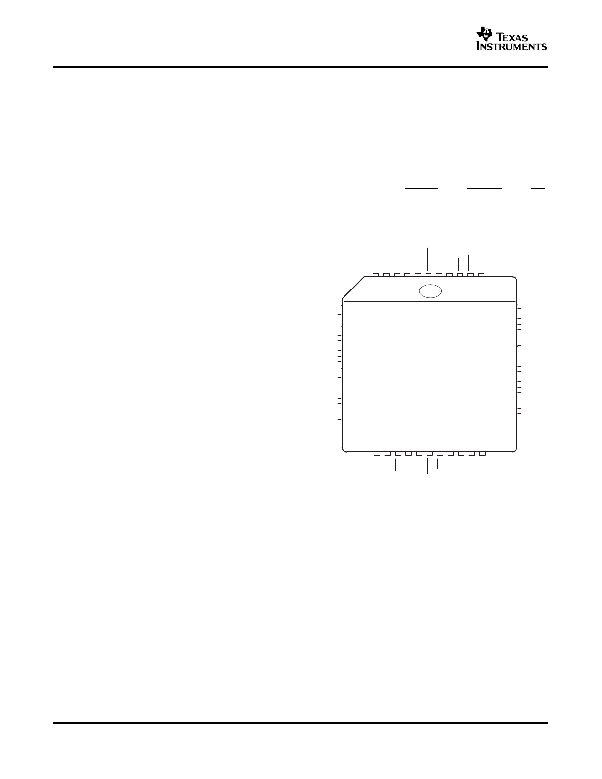
RXA
MFA
D5
D6
RIB
DSRB
CDB
TXRDYB
V
CC
INTA
RTSA
DTRA
TXA
39
35
31
29
30
32
33
34
36
37
38
246 1 42 4041434435
7
8
9
10
11
12
13
14
15
16
17
1918 26 2820 21 22 23 24 25 27
A0
XTAL1
GND
XTAL2
A1
A2
CHSEL
INTB
D7
IOW
CS
MFB
RESET
GND
RTSB
IOR
RXB
TXB
DTRB
CTSB
D4
D0
CDA
CTSA
DSRA
RIA
V
CC
TXRDYA
D1
D2
D3
TL16C2752FN
FN PACKAGE
(TOP VIEW)
TL16C2752
SLWS188 – JUNE 2006
DESCRIPTION
The TL16C2752 is a speed and functional upgrade
of the TL16C2552. Since they are pinout and
software compatible, designs can easily migrate from
the TL16C2552 to the TL16C2752 if needed. The
additional functionality within the TL16C2752 is
accessed via an extended register set. Some of the
key new features are larger receive and transmit
fifos, embedded IrDA encoders and decoders,
RS-485 transceiver controls, software flow control
(Xon/Xoff) modes, programmable transmit fifo
thresholds, extended receive and transmit threshold
levels for interrupts, and extended receive threshold
levels for flow control halt/resume operation.
The TL16C2752 is a dual universal asynchronous
receiver and transmitter (UART). It incorporates the
functionality of two independent UARTs, each UART
having its own register set and transmit and receive
FIFOs. The two UARTs share only the data bus
interface and clock source, otherwise they operate
independently. Another name for the UART function
is Asynchronous Communications Element (ACE),
and these terms will be used interchangeably. The
bulk of this document describes the behavior of each
ACE, with the understanding that two such devices
are incorporated into the TL16C2752.
Functionally equivalent to the TL16C450 on power
up or reset (single character or TL16C450 mode),
each ACE can be placed in an alternate FIFO mode.
This relieves the CPU of excessive software
overhead by buffering received and to be transmitted
characters. Each receiver and transmitter store up to
64 bytes in their respective FIFOs, with the receive
FIFO including three additional bits per byte for error
status. In the FIFO mode, selectable hardware or
software autoflow control features can significantly
reduce program overload and increase system
efficiency by automatically controlling serial data
flow.
Each ACE performs serial-to-parallel conversions on
data received from a peripheral device or modem
and stores the parallel data in its receive buffer or
FIFO, and each ACE performs parallel-to-serial
conversions on data sent from its CPU after storing
the parallel data in its transmit buffer or FIFO. The
CPU can read the status of either ACE at any time.
Each ACE includes complete modem control
capability and a processor interrupt system that can
be tailored to the application.
2
Each ACE includes a programmable baud rate
generator capable of dividing a reference clock with
divisors of from 1 to 65535, thus producing a 16× or
8× internal reference clock for the transmitter and
receiver logic. Each ACE accommodates up to a
3-Mbaud serial data rate (48-MHz input clock). As a
reference point, that speed would generate a 333-ns
bit time and a 3.33-µs character time (for 8,N,1 serial
data), with the internal clock running at 48 MHz and
16× sampling.
Each ACE has a TXRDY and RXRDY (via MF)
output that can be used to interface to a DMA
controller.
Submit Documentation Feedback
www.ti.com
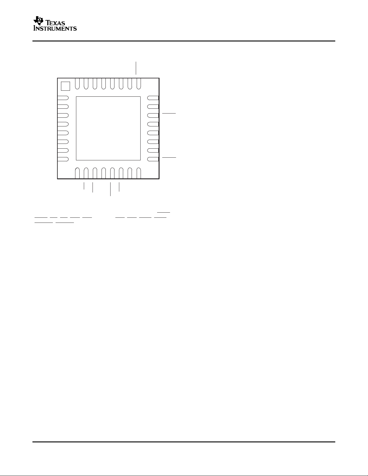
INTB
CS
IOW
RESET
RTSB
IOR
RXB
TXB
1
2
3
4
5
6
7
8
9
10
11
12
13
14
15
16
24
23
22
21
20
19
18
17
D6
D7
A0
XTAL1
XTAL2
A1
A2
CHSEL
RXA
TXA
RTSA
INTA
GND
NC
NC
CTSB
32
31
30
29
28
27
26
25
D5D4D3D2D1D0V
CC
CTSA
RHB PACKAGE
(TOP VIEW)
NC − No internal connection
NOTE: The 32-pin RHB package does not provide access to DSRA
,
DSRB, RIA, RIB, CDA, CDB inputs and MFA, MFB, DTRA , DTRB,
TXRDYA
, TXRDYB outputs.
TL16C2752RHB
TL16C2752
SLWS188 – JUNE 2006
Submit Documentation Feedback
3
www.ti.com
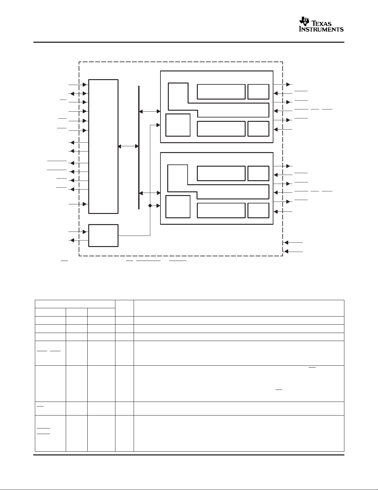
PRODUCT PREVIEW
Crystal
OSC
Buffer
Data Bus
Interface
A2 − A0
D7 − D0
CS
CHSEL
IOR
IOW
INTA
INTB
TXRDYA
TXRDYB
MFA
MFB
RESET
XTAL1
XTAL2
BAUD
Rate
Gen
64 Byte Tx FIFO
64 Byte Rx FIFO
Tx
IR ENC
UART Channel A
BAUD
Rate
Gen
64 Byte Tx FIFO
64 Byte Rx FIFO
UART Channel B
CTSA
DTRA
DSRA, RIA, CDA
RTSA
CTSB
DTRB
DSRB, RIB, CDB
RTSB
V
CC
GND
TXA
RXA
TXB
RXB
UART Regs
UART Regs
Rx
IR DEC
Tx
IR ENC
Rx
IR DEC
TL16C2752
SLWS188 – JUNE 2006
TL16C2752 Block Diagram
A. MF output allows selection of OP, BAUDOUT, or RXRDY per channel.
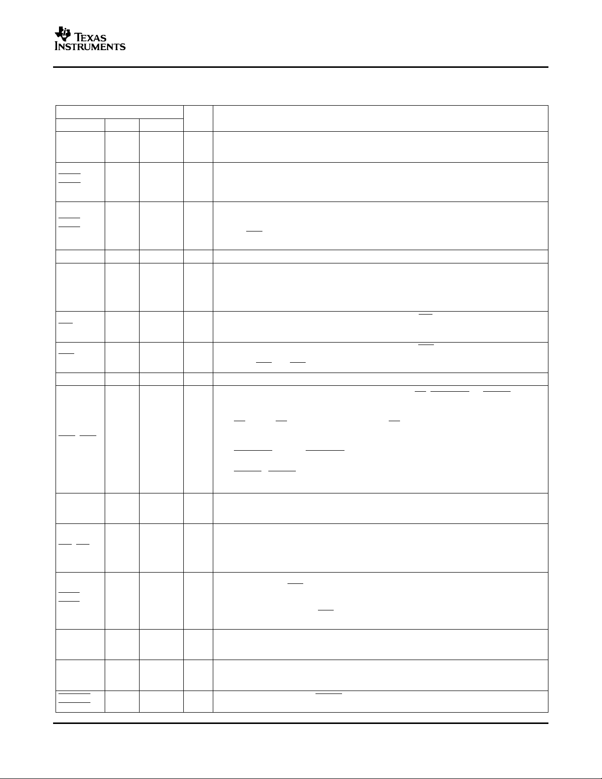
TERMINAL
NAME FN NO. RHB NO.
A0 10 3 I Address 0 select bit. Internal registers address selection
A1 14 6 I Address 1 select bit. Internal registers address selection
A2 15 7 I Address 2 select bit. Internal registers address selection
CDA, CDB 42, 30 – I
CHSEL 16 8 I
CS 18 10 I
CTSA, data from the 2552. Status can be tested by reading MSR bit 4. These pins only affect the
CTSB transmit and receive operations when auto CTS function is enabled through the enhanced
40, 28 25, 17 I
DEVICE INFORMATION
TERMINAL FUNCTIONS
I/O DESCRIPTION
Carrier detect (active low). These inputs are associated with individual UART channels A and
B. A low on these pins indicates that a carrier has been detected by the modem for that
channel. The state of these inputs is reflected in the modem status register (MSR). These
inputs should be pulled high if unused.
Channel select. UART channel A or B is selected by the state of this pin when CS is a logic 0.
A logic 0 on the CHSEL selects the UART channel B while a logic 1 selects UART channel A.
CHSEL could just be an address line from the user CPU such as A3. Bit 0 of the alternate
function register (AFR) can temporarily override CHSEL function, allowing the user to write to
both channel register simultaneously with one write cycle when CS is low. It is especially
useful during the initialization routine.
UART chip select (active low). This pin selects channel A or B in accordance with the state of
the CHSEL pin. This allows data to be transferred between the user CPU and the 2552.
Clear to send (active low). These inputs are associated with individual UART channels A and
B. A logic low on the CTS pins indicates the modem or data set is ready to accept transmit
feature register (EFR) bit 7, for hardware flow control operation. These inputs should be
pulled high if unused.
4
Submit Documentation Feedback
www.ti.com
TL16C2752
SLWS188 – JUNE 2006
DEVICE INFORMATION (continued)
TERMINAL FUNCTIONS (continued)
TERMINAL
NAME FN NO. RHB NO.
D0-D4 2 - 6 27 - 31 Data bus (bidirectional). These pins are the eight bit, 3-state data bus for transferring
D5-D7 7 - 9 32, 1, 2
DSRA, and B. A logic low on these pins indicates the modem or data set is powered on and is ready
DSRB for data exchange with the UART. The state of these inputs is reflected in the modem status
DTRA,
DTRB
GND 12, 22 20 Signal and power ground.
INTA, INTB 34, 17 21, 9 O the interrupt enable register (IER). Interrupt conditions include: receiver errors, available
IOR 24 14 I internal register defined by address bits A0-A2 onto the TL16C2552 data bus (D0-D7) for
IOW 20 11 I data bus (D0-D7) from the external CPU to an internal register that is defined by address bits
NC – 18, 19 No internal connection
MFA, MFB 35, 19 – O
RESET 21 12 I output and the receiver input will be disabled during reset time. See TL16C2552 external
RIA, RIB 43, 31 – I telephone line. A low to high transition on these input pins generates a modem status
RTSA, Writing a 1 in the modem control register (MCR bit 1) sets these pins to low, indicating data is
RTSB available. After a reset, these pins are set to high. These pins only affects the transmit and
RXA, RXB 39, 25 24, 15 I 2552. During the local loopback mode, these RX input pins are disabled and TX data is
TXA, TXB 38, 26 23, 16 O the 2552. During the local loopback mode, the TX input pin is disabled and TX data is
TXRDYA, Transmit ready (active low). TXRDY A and B go low when there are at least a trigger level
TXRDYB numbers of spaces available. They go high when the TX buffer is full.
41, 29 – I
37, 27 – O These pins can be controlled through the modem control register. Writing a 1 to MCR bit 0
36, 23 22, 13 O
1, 32 – O
I/O DESCRIPTION
I/O information to or from the controlling CPU. D0 is the least significant bit and the first data bit in
a transmit or receive serial data stream.
Data set ready (active low). These inputs are associated with individual UART channels A
register (MSR). These inputs should be pulled high if unused.
Data terminal ready (active low). These outputs are associated with individual UART channels
A and B. A logic low on these pins indicates that theTLl16C2552 is powered on and ready.
sets the DTR output to low, enabling the modem. The output of these pins is high after writing
a 0 to MCR bit 0, or after a reset.
Interrupt A and B (active high). These pins provide individual channel interrupts, INT A and B.
INT A and B are enabled when MCR bit 3 is set to a logic 1, interrupt sources are enabled in
receiver buffer data, available transmit buffer space or when a modem status flag is detected.
INTA-B are in the high-impedance state after reset.
Read input (active low strobe). A high to low transition on IOR will load the contents of an
access by an external CPU.
Write input (active low strobe). A low to high transition on IOW will transfer the contents of the
A0-A2 and CSA and CSB
Multi-function output. This output pin can function as the OP, BAUDOUT, or RXRDY pin. One
of these output signal functions can be selected by the user programmable bits 1-2 of the
alternate function register (AFR). These signal functions are described as follows:
1. OP - When OP (active low) is selected, the MF pin is a logic 0 when MCR bit 3 is set to
a logic 1 (see MCR bit 3). MCR bit 3 defaults to a logic 1 condition after a reset or
power-up.
2. BAUDOUT - When BAUDOUT function is selected, the 16× baud rate clock output is
available at this pin.
3. RXRDY - RXRDY (active low) is intended for monitoring DMA data transfers.
If it is not used, leave it unconnected.
Reset. RESET will reset the internal registers and all the outputs. The UART transmitter
reset conditions for initialization details. RESET is an active-high input.
Ring indicator (active low). These inputs are associated with individual UART channels A and
B. A logic low on these pins indicates the modem has received a ringing signal from the
interrupt, if enabled. The state of these inputs is reflected in the modem status register (MSR).
These inputs should be pulled high if unused.
Request to send (active low). These outputs are associated with individual UART channels A
and B. A low on the RTS pin indicates the transmitter has data ready and waiting to send.
receive operation when auto RTS function is enabled through the enhanced feature register
(EFR) bit 6, for hardware flow control operation.
Receive data input. These inputs are associated with individual serial channel data to the
internally connected to the UART RX input internally.
Transmit data. These outputs are associated with individual serial transmit channel data from
internally connected to the UART RX input.
Submit Documentation Feedback
5
www.ti.com
PRODUCT PREVIEW
RCV
FIFO
Serial to
Parallel
Flow
Control
XMT
FIFO
Parallel
to Serial
Flow
Control
Parallel
to Serial
Flow
Control
Serial to
Parallel
Flow
Control
XMT
FIFO
RCV
FIFO
ACE1 ACE2
D7−D0
RX TX
RTS CTS
TX RX
CTS RTS
D7−D0
TL16C2752
SLWS188 – JUNE 2006
DEVICE INFORMATION (continued)
TERMINAL FUNCTIONS (continued)
TERMINAL
NAME FN NO. RHB NO.
V
CC
XTAL1 11 4 I
XTAL2 13 5 O
33, 44 26 I Power supply inputs.
Detailed Description
Hardware Autoflow Control (see Figure 1 )
Hardware Autoflow control is comprised of auto- CTS and auto- RTS. With auto- CTS, the CTS input must be
active before the transmitter FIFO can emit data. With auto- RTS, RTS becomes active when the receiver needs
more data and notifies the sending serial device. When RTS is connected to CTS, data transmission does not
occur unless the receiver FIFO has space for the data; thus, overrun errors are eliminated using ACE1 and
ACE2 from a TLC16C2752 with the autoflow control enabled. If not, overrun errors can occur when the transmit
data rate exceeds the receiver FIFO read latency.
I/O DESCRIPTION
Crystal or external clock input. XTAL1 functions as a crystal input or as an external clock
input. A crystal can be connected between XTAL1 and XTAL2 to form an internal oscillator
circuit (see Figure 4 ). Alternatively, an external clock can be connected to XTAL1 to provide
custom data rates.
Output of the crystal oscillator or buffered clock. See also XTAL1. XTAL2 is used as a crystal
oscillator output or buffered a clock output.
Figure 1. Autoflow Control (Auto- RTS and Auto- CTS) Example
Auto- RTS (See Figure 2 and Figure 3 )
Auto- RTS data flow control originates in the receiver timing and control block (see functional block diagram) and
is linked to the programmed receiver FIFO trigger level. When the receiver FIFO level reaches the defined halt
trigger level 8 (see Figure 3 ), RTS is deasserted. The sending ACE may send an additional byte after the trigger
level is reached (assuming the sending ACE has another byte to send) because it may not recognize the
deassertion of RTS until after it has begun sending the additional byte. RTS is automatically reasserted once the
defined resume trigger level is reached.
Auto- CTS (See Figure 2 )
The transmitter circuitry checks CTS before sending the next data byte. When CTS is active, it sends the next
byte. To stop the transmitter from sending the following byte, CTS must be released before the middle of the last
stop bit that is currently being sent (see Figure 2 ). The auto- CTS function reduces interrupts to the host system.
When flow control is enabled, CTS level changes do not trigger host interrupts because the device automatically
controls its own transmitter. Without auto- CTS, the transmitter sends any data present in the transmit FIFO and
a receiver overrun error may result.
6
Submit Documentation Feedback
www.ti.com
Auto- CTS and Auto- RTS Functional Timing
Start Bits 0−7 Start Bits 0−7 Start Bits 0−7
Stop Stop Stop
SOUT
CTS
Start Byte N Start Byte N+1 Start Byte
Stop Stop Stop
SIN
RTS
RD
(RD RBR)
1 2
N N+1
Figure 2. CTS Functional Timing Waveforms
Figure 3. RTS Functional Timing Waveforms
TL16C2752
SLWS188 – JUNE 2006
Submit Documentation Feedback
7
www.ti.com
PRODUCT PREVIEW
Receiver
Buffer
Register
Divisor
Latch (LS)
Divisor
Latch (MS)
Baud
Generator
Receiver
FIFO
Line
Status
Register
Transmitter
Holding
Register
Modem
Control
Register
Modem
Status
Register
Line
Control
Register
Transmitter
FIFO
Interrupt
Enable
Register
Interrupt
Identification
Register
FIFO
Control
Register
Select
and
Control
Logic
Interrupt
Control
Logic
S
e
l
e
c
t
Data
Bus
Buffer
RXA, B
TXA, B
CTSA, B
DTRA, B
DSRA, b
CDA,B
RIA, B
INTA, B
40, 28
37, 27
41, 29
42, 30
43, 31
34, 17
38, 26
39, 25
A0
10
D(7−0)
9−2
Internal
Data Bus
14
15
18
16
13
21
24
20
11
1
35
A1
A2
CS
CHSEL
XTAL2
RESET
IOR
IOW
XTAL1
TXRDYA
MFA
S
e
l
e
c
t
Receiver
Shift
Register
IrDA Decoder
Receiver
Timing and
Control
Transmitter
Timing and
Control
Modem
Control
Logic
8
33, 44
12, 22
V
CC
GND
Power
Supply
RTSA, B
36, 23
Autoflow
Control
(AFE)
8
8
8
8
8
8
8
32
19
TXRDYB
MFB
Crystal
OSC
Buffer
Transmitter
Shift
Register
IrDA Encoder
TL16C2752
SLWS188 – JUNE 2006
A. Pin numbers shown are for 44-pin PLCC FN package.
8
Figure 4. Functional Block Diagram
Submit Documentation Feedback

www.ti.com
SLWS188 – JUNE 2006
ABSOLUTE MAXIMUM RATINGS
(1)
over operating free-air temperature range (unless otherwise noted)
UNIT
Supply voltage range, V
Input voltage range at any input, V
Output voltage range, V
(2)
CC
I
O
-0.5 V to 7 V
-0.5 V to 7 V
-0.5 V to 7 V
Operating free-air temperature, TA, TL16C2552 0°C to 70°C
Operating free-air temperature, TA, TL16C2552I -40°C to 85°C
Storage temperature range, T
stg
-65°C to 150°C
Lead temperature 1,6 mm (1/16 inch) from case for 10 seconds 260°C
(1) Stresses beyond those listed under "absolute maximum ratings" may cause permanent damage to the device. These are stress ratings
only, and functional operation of the device at these or any other conditions beyond those indicated under "recommended operating
conditions" is not implied. Exposure to absolute-maximum-rated conditions for extended periods may affect device reliability.
(2) All voltage values are with respect to VSS.
RECOMMENDED OPERATING CONDITIONS
over operating free-air temperature range (unless otherwise noted)
1.8 V ±10% MIN NOM MAX UNIT
V
CC
V
I
V
IH
V
IL
V
O
I
OH
I
OL
Supply voltage 1.62 1.8 1.98 V
Input voltage 0 V
CC
High-level input voltage 1.4 1.98 V
Low-level input voltage -0.3 0.4 V
Output voltage 0 V
CC
High-level output current (all outputs) 0.5 mA
Low-level output current (all outputs) 1 mA
Oscillator/clock speed 10 MHz
TL16C2752
V
V
2.5 V ±10% MIN NOM MAX UNIT
V
CC
V
I
V
IH
V
IL
V
O
I
OH
I
OL
Supply voltage 2.25 2.5 2.75 V
Input voltage 0 V
CC
High-level input voltage 1.8 2.75 V
Low-level input voltage -0.3 0.6 V
Output voltage 0 V
CC
High-level output current (all outputs) 1 mA
Low-level output current (all outputs) 2 mA
Oscillator/clock speed 16 MHz
3.3 V ±10% MIN NOM MAX UNIT
V
CC
V
I
V
IH
V
IL
V
O
I
OH
I
OL
Supply voltage 3 3.3 3.6 V
Input voltage 0 V
High-level input voltage 0.7V
CC
Low-level input voltage 0.3V
Output voltage 0 V
CC
CC
CC
High-level output current (all outputs) 1.8 mA
Low-level output current (all outputs) 3.2 mA
Oscillator/clock speed 20 MHz
5 V ±10% MIN NOM MAX UNIT
V
CC
V
I
Supply voltage 4.5 5 5.5 V
Input voltage 0 V
CC
V
V
V
V
V
V
V
Submit Documentation Feedback
9
www.ti.com
PRODUCT PREVIEW
TL16C2752
SLWS188 – JUNE 2006
RECOMMENDED OPERATING CONDITIONS (continued)
over operating free-air temperature range (unless otherwise noted)
5 V ±10% MIN NOM MAX UNIT
V
IH
V
IL
V
O
I
OH
I
OL
ELECTRICAL CHARACTERISTICS
over recommended ranges of supply voltage and operating free-air temperature (unless otherwise noted)
V
High-level output voltage
OH
V
Low-level output voltage
OL
I
Input current V
I
I
High-impedance-state output V
OZ
current mode or chip deselected
I
Supply current V
CC
C
Clock input impedance 15 20 pF
i(CL
K)
C
Clock output impedance 20 30 pF
O(C
LK)
C
Input impedance 6 10 pF
I
C
Output impedance 10 20 pF
O
(1) All typical values are at V
(2) These parameters apply for all outputs except XTAL2.
High-level input voltage All except XTAL1, XTAL2 2 V
XTAL1, XTAL2 0.7V
CC
Low-level input voltage All except XTAL1, XTAL2 0.8 V
XTAL1, XTAL2 0.3V
Output voltage 0 V
High-level output current (all outputs) 4 mA
Low-level output current (all outputs) 4 mA
Oscillator/clock speed 24 MHz
1.8 V Nominal
PARAMETER TEST CONDITIONS MIN TYP
(2)
(2)
IOH= -0.5 mA 1.3 V
IOL= 1 mA 0.5 V
= 1.98 V, V
CC
floating
= 1.98 V, V
CC
= 1.98 V, TA= 0°C, RXA, RXB, DSRA, DSRB, CDA, CDB, mA
CC
CTSA, CTSB, RIA, and RIB at 1.4 V, All other inputs at 0.4 V,
= 0, VI= 0 to 1.98 V, All other terminals 10 µA
SS
= 0, VI= 0 to 1.98 V, Chip selected in write ±20 µA
SS
XTAL1 at 16 MHz, No load on outputs
V
CC
TA= 25°C, All other terminals grounded
= 1.8 V and TA= 25°C.
CC
= 0, V
= 0, f = 1 MHz,
SS
CC
CC
(1)
V
MAX UNIT
ELECTRICAL CHARACTERISTICS
over recommended ranges of supply voltage and operating free-air temperature (unless otherwise noted)
2.5 V Nominal
PARAMETER TEST CONDITIONS MIN TYP
V
V
I
I
I
OZ
I
CC
(1) All typical values are at V
(2) These parameters apply for all outputs except XTAL2.
10
High-level output voltage
OH
Low-level output voltage
OL
Input current V
High-impedance-state output V
current write mode or chip deselected
Supply current V
CC
ADDED SPACE
(2)
IOH= -1 mA 1.8 V
(2)
IOL= 2 mA 0.5 V
= 2.75 V, V
CC
floating
= 2.75 V, V
CC
= 2.75 V, TA= 0°C, RXA, RXB, DSRA, DSRB, CDA, mA
CC
CDB, CTSA, CTSB, RIA, and RIB at 1.8 V, All other inputs at
0.6 V, XTAL1 at 24 MHz, No load on outputs
= 2.5 V and TA= 25°C.
= 0, VI= 0 to 2.75 V, All other terminals 10 µA
SS
= 0, VI= 0 to 2.75 V, Chip selected in ±20 µA
SS
Submit Documentation Feedback
(1)
MAX UNIT

www.ti.com
ELECTRICAL CHARACTERISTICS (continued)
over recommended ranges of supply voltage and operating free-air temperature (unless otherwise noted)
2.5 V Nominal
PARAMETER TEST CONDITIONS MIN TYP
C
C
C
C
Clock input impedance 15 20 pF
i(CLK)
Clock output impedance 20 30 pF
O(CLK)
Input impedance 6 10 pF
I
Output impedance 10 20 pF
O
V
= 0, V
CC
TA= 25°C, All other terminals grounded
= 0, f = 1 MHz,
SS
ELECTRICAL CHARACTERISTICS
over recommended ranges of supply voltage and operating free-air temperature (unless otherwise noted)
3.3 V Nominal
PARAMETER TEST CONDITIONS MIN TYP
V
OH
V
OL
I
I
I
OZ
I
CC
C
i(CLK)
C
O(CLK)
C
I
C
O
High-level output voltage
Low-level output voltage
Input current V
High-impedance-state output V
current write mode or chip deselected
Supply current V
Clock input impedance 15 20 pF
Clock output impedance 20 30 pF
Input impedance 6 10 pF
Output impedance 10 20 pF
(1) All typical values are at V
(2) These parameters apply for all outputs except XTAL2.
(2)
(2)
= 3.3 V and TA= 25°C.
CC
IOH= -1.8 mA 2.4 V
IOL= 3.2 mA 0.5 V
= 3.6 V, V
CC
floating
= 3.6 V, V
CC
= 3.6 V, TA= 0°C, RXA, RXB, DSRA, DSRB, CDA, mA
CC
CDB, CTSA, CTSB, RIA, and RIB at 2 V, All other inputs
= 0, VI= 0 to 3.6 V, All other terminals 10 µA
SS
= 0, VI= 0 to 3.6 V, Chip selected in ±20 µA
SS
at 0.8 V, XTAL1 at 32 MHz, No load on outputs
V
= 0, V
CC
TA= 25°C, All other terminals grounded
= 0, f = 1 MHz,
SS
TL16C2752
SLWS188 – JUNE 2006
(1)
MAX UNIT
(1)
MAX UNIT
Submit Documentation Feedback
11

www.ti.com
PRODUCT PREVIEW
TL16C2752
SLWS188 – JUNE 2006
ELECTRICAL CHARACTERISTICS
over recommended ranges of supply voltage and operating free-air temperature (unless otherwise noted)
5 V Nominal
PARAMETER TEST CONDITIONS MIN TYP
V
V
I
I
I
OZ
I
CC
C
C
C
C
High-level output voltage
OH
Low-level output voltage
OL
Input current V
High-impedance-state output V
current write mode or chip deselected
Supply current V
Clock input impedance 15 20 pF
i(CLK)
Clock output impedance 20 30 pF
O(CLK)
Input impedance 6 10 pF
I
Output impedance 10 20 pF
O
(1) All typical values are at V
(2) These parameters apply for all outputs except XTAL2.
(2)
(2)
= 5 V and TA= 25°C.
CC
IOH= -4 mA 4 V
IOL= 4 mA 0.4 V
= 5.5 V, V
CC
terminals floating
= 5.5 V, V
CC
= 5.5 V, TA= 0°C, RXA, RXB, DSRA, DSRB, mA
CC
CDA, CDB, CTSA, CTSB, RIA, and RIB at 2 V, All
= 0, VI= 0 to 5.5 V, All other 10 µA
SS
= 0, VI= 0 to 5.5 V, Chip selected in ±20 µA
SS
other inputs at 0.8 V, XTAL1 at 48 MHz, No load on
outputs
V
= 0, V
CC
TA= 25°C, All other terminals grounded
= 0, f = 1 MHz,
SS
(1)
MAX UNIT
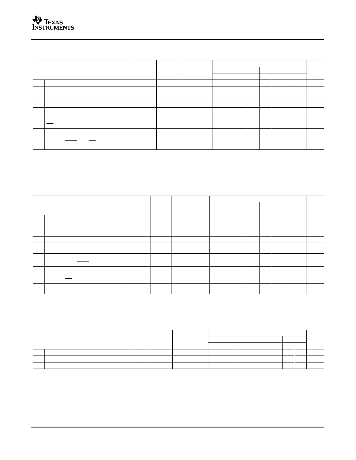
TIMING REQUIREMENTS
over recommended ranges of supply voltage and operating free-air temperature (unless otherwise noted)
PARAMETER FIGURE 1.8 V 2.5 V 3.3 V 5 V UNIT
t
Pulse duration, RESET t
w8
t
Pulse duration, clock high t
w1
t
Pulse duration, clock low t
w2
t
Cycle time, read (tw7+ td8+ th7) RC 8 115 80 62 57 ns
cR
t
Cycle time, write (tw6+ td5+ th4) WC 7 115 80 62 57 ns
cW
t
Pulse duration, IOW or CS t
w6
t
Pulse duration, IOR or CS t
w7
t
Setup time, data valid before IOW↑ or CS↑ t
SU3
t
Hold time, address valid after IOW↑ or CS↑ t
h4
t
Hold time, data valid after IOW↑ or CS↑ t
h5
t
Hold time, data valid after IOR↑ or CS↑ t
h7
t
Delay time, address valid before IOW↓ or CS↓ t
d5
t
Delay time, address valid to IOR↓ or CS↓ t
d8
t
Delay time, IOR↓ or CS↓ to data valid t
d10
t
Delay time, IOR↑ or CS↑ to floating data t
d11
t
Write cycle to write cycle delay 7 100 75 60 50 ns
d12
t
Read cycle to read cycle delay 8 100 75 60 50 ns
d13
BAUD GENERATOR SWITCHING CHARACTERISTICS
over recommended ranges of supply voltage and operating free-air temperature, CL= 30 pF (for FN package only)
PARAMETER FIGURE 1.8 V 2.5 V 3.3 V 5 V UNIT
t
Pulse duration, BAUDOUT low t
w3
t
Pulse duration, BAUDOUT high t
w4
t
Delay time, XIN ↑ to BAUDOUT↑ t
d1
t
Delay time, XIN ↑ ↓ to BAUDOUT↓ t
d2
ALT. TEST
SYMBOL CONDITIONS
RESET
XH
XL
IOW
IOR
DS
WA
DH
RA
AW
AR
RVD
HZ
ALT. TEST
SYMBOL CONDITIONS
LW
HW
BLD
BHD
6 25 16 12 8 ns
7 80 55 45 40 ns
8 80 55 45 40 ns
7 25 20 15 15 ns
7 20 15 10 10 ns
7 15 10 5 5 ns
8 20 15 10 10 ns
7 15 10 7 7 ns
8 15 10 7 7 ns
8 CL= 30 pF 55 35 25 20 ns
8 CL= 30 pF 40 30 20 20 ns
6 CLK ÷ 2 50 35 27 16 ns
6 CLK ÷ 2 50 35 27 16 ns
6 35 25 20 15 ns
6 35 25 20 15 ns
LIMITS
MIN MAX MIN MAX MIN MAX MIN MAX
1 1 1 1 µs
LIMITS
MIN MAX MIN MAX MIN MAX MIN MAX
12
Submit Documentation Feedback
www.ti.com
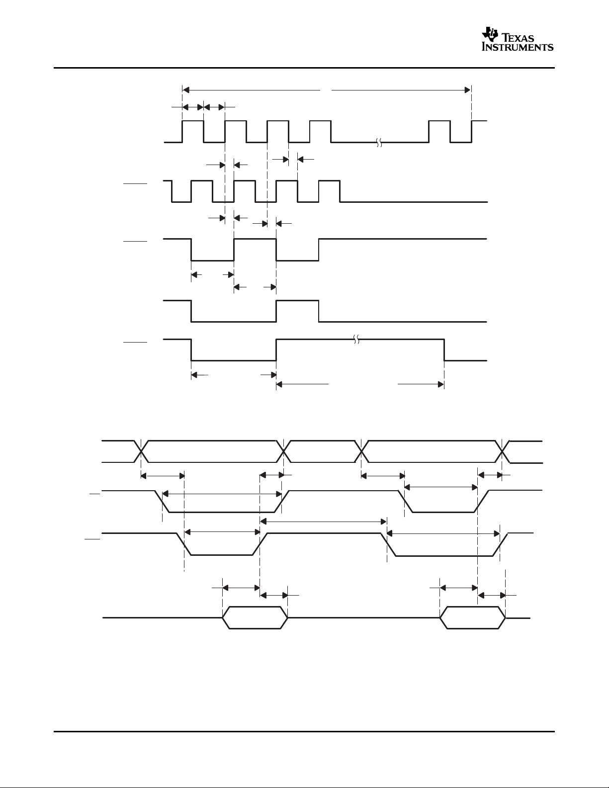
RECEIVER SWITCHING CHARACTERISTICS
over recommended ranges of supply voltage and operating free-air temperature (unless otherwise noted)
PARAMETER FIGURE 1.8 V 2.5 V 3.3 V 5 V UNIT
t
Delay time, RCLK to sample t
d12
t
Delay time, stop to set INT or read RBR to LSI t
d13
interrupt or stop to RXRDY↓ 11, 12 cycle
t
Delay time, read RBR/LSR to reset INT t
d14
t
Delay time, RCV threshold byte to RTS↑ 19 CL= 30 pF 2 baudout
d26
t
Delay time, read of last byte in receive FIFO to 19 CL= 30 pF 2 baudout
d27
RTS↓ cycles
t
Delay time, first data bit of 16th character to RTS↑ 20 CL= 30 pF 2 baudout
d28
t
Delay time, RBRRD low to RTS↓ 20 CL= 30 pF 2 baudout
d29
ALT. TEST
SYMBOL CONDITIONS
SCD
SINT
RINT
9 20 15 10 10 ns
8, 9, 10, 1 1 1 1 RCLK
8, 9, 10, CL= 30 pF 100 90 80 70 ns
11, 12
MIN MAX MIN MAX MIN MAX MIN MAX
(1) In the FIFO mode, the read cycle (RC) = 1 baudclock (min) between reads of the receive FIFO and the status registers (interrupt
identification register or line status register).
(2) A baudout cycle is equal to the period of the input clock divided by the programmed divider in DLL, DLM.
LIMITS
TRANSMITTER SWITCHING CHARACTERISTICS
over recommended ranges of supply voltage and operating free-air temperature (unless otherwise noted)
PARAMETER ALT. SYMBOL FIGURE 1.8 V 2.5 V 3.3 V 5 V UNIT
t
Delay time, initial write to transmit start t
d15
t
Delay time, start to INT t
d16
t
Delay time, IOW (WR THR) to reset INT t
d17
t
Delay time, initial write to INT (THRE
d18
t
Delay time, read IOR↑ to reset INT (THRE
d19
t
Delay time, write to TXRDY inactive t
d20
t
Delay time, start to TXRDY active t
d21
t
Setup time, CTS↑ before midpoint of stop bit 18 30 20 10 10 ns
SU4
t
Delay time, CTS low to TX ↓ 18 CL= 30 pF 24 24 24 24 baudout
d25
(1)
) t
(1)
) t
IRS
STI
HR
SI
IR
WXI
SXA
14 8 24 8 24 8 24 8 24 baudout
14 8 10 8 10 8 10 8 10 baudout
14 CL= 30 pF 70 60 50 50 ns
14 16 34 16 34 16 34 16 34 baudout
14 CL= 30 pF 70 50 35 35 ns
15, 16 CL= 30 pF 60 45 35 35 ns
15, 16 CL= 30 pF 9 9 9 9 baudout
TEST
CONDITIONS
MIN MAX MIN MAX MIN MAX MIN MAX
(1) THRE = Transmitter Holding Register Empty; IIR = Interrupt Identification Register.
LIMITS
TL16C2752
SLWS188 – JUNE 2006
(1)
(2)
cycles
cycles
cycles
cycles
cycles
cycles
cycles
cycles
MODEM CONTROL SWITCHING CHARACTERISTICS
over operating free-air temperature range (unless otherwise noted)
PARAMETER FIGURE 1.8 V 2.5 V 3.3 V 5 V UNIT
t
Delay time, WR MCR to output t
d22
t
Delay time, modem interrupt to set INT t
d23
t
Delay time, RD MSR to reset INT t
d24
ALT. TEST
SYMBOL CONDITIONS
MDO
SIM
RIM
Submit Documentation Feedback
LIMITS
MIN MAX MIN MAX MIN MAX MIN MAX
17 CL= 30 pF 90 70 60 50 ns
17 CL= 30 pF 60 50 40 35 ns
17 CL= 30 pF 80 60 50 40 ns
13
www.ti.com
PRODUCT PREVIEW
MFA,B
(1/1)
XTAL
MFA,B
(1/2)
MFA,B
(1/3)
MFA,B
(1/N)
(N > 3)
t
d2
t
d1
t
d2
t
w1
t
w2
t
d1
2 XIN Cycles
t
w3
t
w4
N
(N−2) XIN Cycles
t
su3
t
h5
Valid Data
Valid Address
CHSEL,
A2−A0
D7−D0
IOW
CS
t
d5
t
w6
t
d12
t
h4
t
su3
t
h5
Valid Data
t
d5
t
h4
t
w6
t
w6
Valid Address
t
w6
TL16C2752
SLWS188 – JUNE 2006
Figure 5. Input Clock and Baud Generator Timing Waveforms
(For FN Package Only) (When AFR2:1 = 01)
Figure 6. Write Cycle Timing Waveforms
14
Submit Documentation Feedback

www.ti.com
t
d10
t
d11
Valid Data
Valid Address
CHSEL,
A2−A0
D7−D0
IOR
CS
t
d8
t
w7
t
d13
t
h7
t
h11
Valid Data
t
d8
t
h7
t
w7
t
w7
Valid Address
t
w7
t
d10
t
d13
Active
Active
IOR
(read RBR)
RCLK
(Internal)
t
d14
t
d14
t
d12
Parity StopStart Data Bits 5−8
Sample Clock
(Internal)
TL16C450 Mode:
Sample Clock
RXA, RXB
INT
(data ready)
INT
(RCV error)
IOR
(read LSR)
50%50%
50%
50%
50%
50%
8 CLKs
Figure 7. Read Cycle Timing Waveforms
TL16C2752
SLWS188 – JUNE 2006
Figure 8. Receiver Timing Waveforms
Submit Documentation Feedback
15

www.ti.com
PRODUCT PREVIEW
t
d13
(see Note A)
t
d14
Stop
Data Bits 5−8
Sample Clock
(Internal)
RXA, RXB
Trigger Level
INT
(FCR6, 7 = 0, 0)
INT
Line Status
Interrupt (LSI)
t
d14
IOR
(RD LSR)
IOR
(RD RBR)
Active
Active
(FIFO at or above
trigger level)
(FIFO below
trigger level)
50%50%
50%
50%
50%
50%
t
d13
(see Note A)
t
d14
Stop
Top Byte of FIFO
Sample Clock
(Internal)
RXA, RXB
Time-Out or
Trigger Level
Interrupt
Line Status
Interrupt (LSI)
t
d13
(FIFO at or above
trigger level)
(FIFO below
trigger level)
IOP
(RD LSR)
IOR
(RD RBR)
Active Active
t
d14
Previous Byte
Read From FIFO
50%
50%
50%50%
50%
50% 50%
TL16C2752
SLWS188 – JUNE 2006
Figure 9. Receive FIFO First Byte (Sets DR Bit) Waveforms
Figure 10. Receive FIFO Bytes Other Than the First Byte (DR Internal Bit Already Set) Waveforms
16
Submit Documentation Feedback

www.ti.com
t
d13
(see Note B)
t
d14
Stop
Sample Clock
(Internal)
RXA, RXB
(first byte)
Active
IOR
(RD RBR)
RXRDYA, RXRDYB
See Note A
50%
50%
50%
t
d13
(see Note B)
t
d14
Sample Clock
(Internal)
RXA, RXB
(first byte that reaches
the trigger level)
Active
IOR
(RD RBR)
RXRDYA, RXRDYB
See Note A
50%
50%50%
t
d16
Parity Stop
Start
Data Bits
TXA, TXB
Start
t
d15
t
d17
t
d17
t
d18
t
d19
INT
(THRE)
IOW
(WR THR)
IOR
50% 50% 50% 50% 50%
50%
50%
50%
50%
50%
50%
TL16C2752
SLWS188 – JUNE 2006
Figure 11. Receiver Ready ( RXRDY) Waveforms, FCR0 = 0 or FCR0 = 1 and FCR3 = 0 (Mode 0)
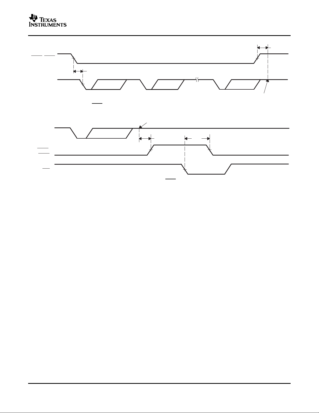
Figure 12. Receiver Ready ( RXRDY) Waveforms, FCR0 = 1 and FCR3 = 1 (Mode 1)
Figure 13. Transmitter Timing Waveforms
Submit Documentation Feedback
17

www.ti.com
PRODUCT PREVIEW
t
d20
IOW
(WR THR)
t
d21
Parity
Stop
Data
Start
Byte 1
TXA, TXB
TXRDYA, TXRDYB
50%
50%
50%
50%
IOW
(WR THR)
Parity
Stop
Data
Start
Byte 16
TXA, TXB
TXRDYA
, TXRDYB
FIFO Full
t
d20
t
d21
50%
50%
50%
50%
IOW
(WR MCR)
RTSA, RTSB, DTRA,
DTRB, OPA, OPB
CTSA, CTSB, DSRA,
DSRB, CDA, CDB
t
d23
t
d24
t
d23
INT
(modem)
IOR
(RD MSR)
RI
50% 50%
50% 50%
50%
50%
50%
50%
50%
50%
t
d22
t
d22
TL16C2752
SLWS188 – JUNE 2006
Figure 14. Transmitter Ready ( TXRDY) Waveforms, FCR0 = 0 or FCR0 = 1 and FCR3 = 0 (Mode 0)
Figure 15. Transmitter Ready ( TXRDY) Waveforms, FCR0 = 1 and FCR3 = 1 (Mode 1)
18
Figure 16. Modem Control Timing Waveforms
Submit Documentation Feedback
www.ti.com
Midpoint of Stop Bit
t
d25
t
su4
CTSA, CTSB
TXA, TXB
50% 50%
50%
t
d27
RXA, RXB
50%
t
d26
50%
50%
Midpoint of Stop Bit
RTSA
,
RTSB
IOR
Figure 17. CTS and TX Autoflow Control Timing (Start and Stop) Waveforms
TL16C2752
SLWS188 – JUNE 2006
Figure 18. Auto- RTS Timing
Submit Documentation Feedback
19

www.ti.com
PRODUCT PREVIEW
Buffer
(Optional)
Address
Decoder
A0−A23
AD0−AD15
RSI/ABT
PHI1 PHI2
PHI1 PHI2
CPU
RSTO
A0−A2
CHSEL
CS
RESET
D0−D7
D0−D7
IOR
IOW
XTAL1
XTAL2
DTRA, B
RTSA, B
RIA, B
CDA, B
DSRA, B
CTSA, B
RXA, B
TXA, B
INTA, B
GND
(VSS)
V
CC
12, 22
33, 44
Alternate
Crystal Control
TL16C2752
EIA-232-D
Connector
20
1
8
6
5
2
3
7
1
11
13
37, 27
36, 23
43, 31
42, 30
41, 29
40, 28
39, 25
34, 17
38, 26
20
24
21
16
18
TCU
WR
RD
(Optional)
10, 14, 15
2−9
33 pF
33 pF
TL16C2752
SLWS188 – JUNE 2006
APPLICATION INFORMATION
A. Pin numbers shown are for 44-pin PLCC FN package.
UART Internal Registers
Each of the UART channel in the 2752 has its own set of configuration registers selected by address lines A0,
A1, and A2 with CS# and CHSEL selecting the channel. The complete register set is shown in Table 1 and
Table 2 .
20
Figure 19. Typical TL16C2752 Connection
PRINCIPLES OF OPERATION
Submit Documentation Feedback

www.ti.com
Table 1. UART Channel A and B UART Internal Registers
ADDRESS RESET (HEX) COMMENTS REGISTER READ/WRITE
A2 - A0
0 0 0 XX RHR = Receive Holding Register Read-only
0 0 0 XX DLL - Div Latch Low Byte Read/Write
0 0 1 XX LCR[7] = 1, LCR ≠ 0xBF DLM - Div Latch High Byte Read/Write
0 1 0 00 AFR - Alternate Function REgister Read/Write
0 0 0 00 DREV - Device Revision Code Read-only
0 0 1 0A DVID - Device Identification Code Read-only
0 0 1 00 LCR[7] = 0 IER - Interrupt Enable Register Read/Write
0 1 0 01 ISR - Interrupt Status Register Read-only
0 1 1 00 LCR = Line Control Register Read/Write
1 0 0 00 MCR - Modem Control Register Read/Write
1 0 1 60 LSR - Line Status Register Read-only
1 1 0 X0 MSR - Modem Status Register Read-only
1 1 1 FF LCR ≠ 0xBF, FCTR[6] = 0 SPR - Scratch Pad Register Read/Write
1 1 1 00 LCR ≠ 0xBF, FCTR[6] = 1 FLVL - RX/TX FIFO Level Counter Register Read-only
1 1 1 80 EMSR - Enhanced Mode Select Register Write-only
0 0 0 00 TRG - RX/TX FIFO Trigger Level Register Write-only
0 0 1 00 FCTR - Feature Control Register Read/Write
0 1 0 00 EFR - Enhanced Function Register Read/Write
1 0 0 00 Xon-1 - Xon Character 1 Read/Write
1 0 1 00 Xon-2 - Xon Character 2 Read/Write
1 1 0 00 Xoff-1 - Xoff Character 1 Read/Write
1 1 1 00 Xoff-2 - Xoff Character 2 Read/Write
VALUE
16C550 Compatible Registers
XX THR - Transmit Holding Register Write-only
00 FCR - FIFO Control Register Write-only
00 FC - RX/TX FIFO Level Counter Register Read-only
LCR[7] = 0
DLL, DLM = 0x00,
LCR[7] = 1, LCR ≠ 0xBF
LCR[7] = 0
LCR ≠ 0xBF Reserved Write-only
Reserved Write-only
Enhanced Registers
LCR = 0xBF
TL16C2752
SLWS188 – JUNE 2006
Table 2. Internal Registers Description
Address Reg Read/
A2 - A0 NAME Write
0 0 0 RHR RD LCR[7] = 0 Bit 7 Bit 6 Bit 5 Bit 4 Bit 3 Bit 2 Bit 1 Bit 0
0 0 0 THR WR Bit 7 Bit 6 Bit 5 Bit 4 Bit 3 Bit 2 Bit 1 Bit 0
0 0 1 IER RD/WR 0/ 0/ 0/ 0/ Modem Stat. RX Line Stat. TX Empty Int. RX Data Int.
0 1 0 ISR RD FIFOs FIFOs 0/ 0/ INT Source INT Source INT Source INT Source
0 1 0 FCR WR RXFIFO RXFIFO 0/ 0/ DMA Mode TX FIFO RX FIFO FIFOs Enable
0 1 1 LCR RD/WR Divisor Set TX Break Set Parity Even Parity Parity Enable Stop Bits Word Length Word Length
1 0 0 MCR RD/WR 0/ 0/ 0/ Internal OP2# Output Rsrvd (OP1#) RTS# Output DTR# Output
1 0 1 LSR RD RX FIFO THR & TSR THR Empty RX Break RX Framing RX Parity RX Overrun RX Data
1 1 0 MSR RD CD# Input RI# Input DSR# Input CTS# Input Delta CD# Delta RI# Delta DSR# Delta CTS#
1 1 1 SPR RD/WR LCR ≠ 0xBF Bit 7 Bit 6 Bit 5 Bit 4 Bit 3 Bit 2 Bit 1 Bit 0
1 1 1 EMSR WR 16X Sampling LSR Error Auto RTS Auto RTS Auto RS485 Rsrvd Rx/Tx FIFO Rx/Tx FIFo
1 1 1 FLVL RD Bit 7 Bit 6 Bit 5 Bit 4 Bit 3 Bit 2 Bit 1 Bit 0
Comments Bit 7 Bit 6 Bit 5 Bit 4 Bit 3 Bit 2 Bit 1 Bit 0
16C550 Compatible Registers
CTS Int. RTS Int. Xoff Int. Sleep Mode
Enable Enable Enable Enable
LCR ≠ 0xBF
FCTR Bit 6 = 0
LDR ≠ 0xBF
FCTR Bit 6 = 1
Enabled Enabled Bit 3 Bit 2 Bit 1 Bit 0
Trigger Trigger Enable Reset Reset
Enable Bit 1 Bit 0
BRG IR Mode XonAny
Prescaler Enable
Global Error Empty Error Error Error Ready
Rate Mode Interrupt Hyst. Bit 3 Hyst Bit 2 Output Count Count
Imd/Dly# Inversion
INT Source INT Source
Bit 5 Bit 4
TXFIFO TXFIFO
Trigger Trigger
Loopback Control Control Control
Enable
(1)
Int. Enable Int. Enable Enable Enable
(1) Shaded bits are accessible when EFR Bit 4 = 1.
Submit Documentation Feedback
21

www.ti.com
PRODUCT PREVIEW
TL16C2752
SLWS188 – JUNE 2006
Table 2. Internal Registers Description (continued)
Address Reg Read/
A2 - A0 NAME Write
0 0 0 DLL RD/WR Bit 7 Bit 6 Bit 5 Bit 4 Bit 3 Bit 2 Bit 1 Bit 0
0 0 1 DLM RD/WR LCR[7] = 1 LCR Bit 7 Bit 6 Bit 5 Bit 4 Bit 3 Bit 2 Bit 1 Bit 0
0 1 0 AFR RD/WR Rsvd Rsvd Rsvd Rsvd Rsvd RXRDY# Baudout# Concurrent
0 0 0 DREV RD LCR[7] = 1 LCR Bit 7 Bit 6 Bit 5 Bit 4 Bit 3 Bit 2 Bit 1 Bit 0
0 0 1 DVID RD 0 0 0 0 1 0 1 0
0 0 0 TRG WR LCR = 0xBF Bit 7 Bit 6 Bit 5 Bit 4 Bit 3 Bit 2 Bit 1 Bit 0
0 0 0 FC RD Bit 7 Bit 6 Bit 5 Bit 4 Bit 3 Bit 2 Bit 1 Bit 0
0 0 1 FCTR RD/WR RX/TX Mode SCPAD Swap Trig Table Bit Trig Table Bit Auto RS485 RX IR Input Auto RTS Auto RTS
0 1 0 EFR RD/WR Auto CTS Auto RTS Special Char Enable Software Flow Software Flow Software Flow Software Flow
1 0 0 XON1 RD/WR Bit 7 Bit 6 Bit 5 Bit 4 Bit 3 Bit 2 Bit 1 Bit 0
1 0 1 XON2 RD/WR Bit 7 Bit 6 Bit 5 Bit 4 Bit 3 Bit 2 Bit 1 Bit 0
1 1 0 XOFF1 RD/WR Bit 7 Bit 6 Bit 5 Bit 4 Bit 3 Bit 2 Bit 1 Bit 0
1 1 1 XOFF2 RD/WR Bit 7 Bit 6 Bit 5 Bit 4 Bit 3 Bit 2 Bit 1 Bit 0
Comments Bit 7 Bit 6 Bit 5 Bit 4 Bit 3 Bit 2 Bit 1 Bit 0
Baud Rate Generator Divisor
≠ 0xBF
Select Select Write
≠ 0xBF DLL =
0x00 DLM =
0x00
Enhanced Registers
1 0 Direction Inv. Hyst Bit 1 Hyst Bit 0
Enable Enable Select IER[7:4], Cntl Bit 3 Cntl Bit 2 Cntl Bit 1 Cntl Bit 0
ISR[5:4],
FCT[5:4],
MCR[7:5]
Control
22
Submit Documentation Feedback

MECHANICAL DATA
MPLC004A – OCT OBER 1994
FN (S-PQCC-J**) PLASTIC J-LEADED CHIP CARRIER
20 PIN SHOWN
Seating Plane
0.004 (0,10)
D
D1
13
4
E1E
8
9
NO. OF
PINS
**
D/E
19
13
18
14
0.032 (0,81)
0.026 (0,66)
0.050 (1,27)
0.008 (0,20) NOM
D1/E1
MINMAXMIN
MAX
D2/E2
MIN
0.180 (4,57) MAX
0.120 (3,05)
0.090 (2,29)
0.020 (0,51) MIN
D2/E2
D2/E2
0.021 (0,53)
0.013 (0,33)
0.007 (0,18)
MAX
M
20
28
44
52
68
84
NOTES: A. All linear dimensions are in inches (millimeters).
B. This drawing is subject to change without notice.
C. Falls within JEDEC MS-018
0.385 (9,78)
0.485 (12,32)
0.685 (17,40)
0.785 (19,94)
0.985 (25,02)
1.185 (30,10)
0.395 (10,03)
0.495 (12,57)
0.695 (17,65)
0.795 (20,19)
0.995 (25,27)
1.195 (30,35)
0.350 (8,89)
0.450 (11,43)
0.650 (16,51)
0.750 (19,05)
0.950 (24,13)
1.150 (29,21)
0.356 (9,04)
0.456 (11,58)
0.656 (16,66)
0.756 (19,20)
0.958 (24,33)
1.158 (29,41)
0.141 (3,58)
0.191 (4,85)
0.291 (7,39)
0.341 (8,66)
0.441 (11,20)
0.541 (13,74)
0.169 (4,29)
0.219 (5,56)
0.319 (8,10)
0.369 (9,37)
0.469 (11,91)
0.569 (14,45)
4040005/B 03/95
POST OFFICE BOX 655303 • DALLAS, TEXAS 75265
1


IMPORTANT NOTICE
Texas Instruments Incorporated and its subsidiaries (TI) reserve the right to make corrections, modifications,
enhancements, improvements, and other changes to its products and services at any time and to discontinue
any product or service without notice. Customers should obtain the latest relevant information before placing
orders and should verify that such information is current and complete. All products are sold subject to TI’s terms
and conditions of sale supplied at the time of order acknowledgment.
TI warrants performance of its hardware products to the specifications applicable at the time of sale in
accordance with TI’s standard warranty. Testing and other quality control techniques are used to the extent TI
deems necessary to support this warranty . Except where mandated by government requirements, testing of all
parameters of each product is not necessarily performed.
TI assumes no liability for applications assistance or customer product design. Customers are responsible for
their products and applications using TI components. To minimize the risks associated with customer products
and applications, customers should provide adequate design and operating safeguards.
TI does not warrant or represent that any license, either express or implied, is granted under any TI patent right,
copyright, mask work right, or other TI intellectual property right relating to any combination, machine, or process
in which TI products or services are used. Information published by TI regarding third-party products or services
does not constitute a license from TI to use such products or services or a warranty or endorsement thereof.
Use of such information may require a license from a third party under the patents or other intellectual property
of the third party, or a license from TI under the patents or other intellectual property of TI.
Reproduction of information in TI data books or data sheets is permissible only if reproduction is without
alteration and is accompanied by all associated warranties, conditions, limitations, and notices. Reproduction
of this information with alteration is an unfair and deceptive business practice. TI is not responsible or liable for
such altered documentation.
Resale of TI products or services with statements different from or beyond the parameters stated by TI for that
product or service voids all express and any implied warranties for the associated TI product or service and
is an unfair and deceptive business practice. TI is not responsible or liable for any such statements.
Following are URLs where you can obtain information on other Texas Instruments products and application
solutions:
Products Applications
Amplifiers amplifier.ti.com Audio www.ti.com/audio
Data Converters dataconverter.ti.com Automotive www.ti.com/automotive
DSP dsp.ti.com Broadband www.ti.com/broadband
Interface interface.ti.com Digital Control www.ti.com/digitalcontrol
Logic logic.ti.com Military www.ti.com/military
Power Mgmt power.ti.com Optical Networking www.ti.com/opticalnetwork
Microcontrollers microcontroller.ti.com Security www.ti.com/security
Low Power Wireless www.ti.com/lpw Telephony www.ti.com/telephony
Video & Imaging www.ti.com/video
Wireless www.ti.com/wireless
Mailing Address: Texas Instruments
Post Office Box 655303 Dallas, Texas 75265
Copyright 2006, Texas Instruments Incorporated
 Loading...