

Page 1

Tiva™ TM4C123GH6PM
ROM USER’S GUIDE
ROM-TM4C123GH6PM-UG-750
Copyright © 2011-2013
Texas Instruments Incorporated
Page 2

Copyright
Copyright © 2011-2013 Texas Instruments Incorporated. All rights reserved. Tiva and TivaWare are trademarks of Texas Instruments Instruments. ARM
and Thumb are registered trademarks and Cortex is a trademark of ARM Limited. Other names and brands may be claimed as the property of others.
Please be aware that an important notice concerning availability, standard warranty, and use in critical applications of Texas Instruments semicon-
ductor products and disclaimers thereto appears at the end of this document.
Texas Instruments
108 Wild Basin, Suite 350
Austin, TX 78746
www.ti.com/tiva- c
Revision Information
This is version 750 of this document, last updated on April 8, 2013.
2 April 8, 2013
Page 3

Table of Contents
Table of Contents
Copyright . . . . . . . . . . . . . . . . . . . . . . . . . . . . . . . . . . . . . . . . . . . . . . . . . . . . . 2
Revision Information . . . . . . . . . . . . . . . . . . . . . . . . . . . . . . . . . . . . . . . . . . . . . . . 2
1 Introduction . . . . . . . . . . . . . . . . . . . . . . . . . . . . . . . . . . . . . . . . . . . . . . . . . 5
2 Boot Loader . . . . . . . . . . . . . . . . . . . . . . . . . . . . . . . . . . . . . . . . . . . . . . . . . 7
2.1 Introduction . . . . . . . . . . . . . . . . . . . . . . . . . . . . . . . . . . . . . . . . . . . . . . . . . . 7
2.2 Serial Interfaces . . . . . . . . . . . . . . . . . . . . . . . . . . . . . . . . . . . . . . . . . . . . . . . 7
2.3 USB Interface . . . . . . . . . . . . . . . . . . . . . . . . . . . . . . . . . . . . . . . . . . . . . . . . 12
3 AES Data Tables . . . . . . . . . . . . . . . . . . . . . . . . . . . . . . . . . . . . . . . . . . . . . . 27
3.1 Introduction . . . . . . . . . . . . . . . . . . . . . . . . . . . . . . . . . . . . . . . . . . . . . . . . . . 27
3.2 Data Structures . . . . . . . . . . . . . . . . . . . . . . . . . . . . . . . . . . . . . . . . . . . . . . . 27
4 Analog Comparator . . . . . . . . . . . . . . . . . . . . . . . . . . . . . . . . . . . . . . . . . . . . 29
4.1 Introduction . . . . . . . . . . . . . . . . . . . . . . . . . . . . . . . . . . . . . . . . . . . . . . . . . . 29
4.2 Functions . . . . . . . . . . . . . . . . . . . . . . . . . . . . . . . . . . . . . . . . . . . . . . . . . . . 29
5 Analog to Digital Converter (ADC) . . . . . . . . . . . . . . . . . . . . . . . . . . . . . . . . . . . . 35
5.1 Introduction . . . . . . . . . . . . . . . . . . . . . . . . . . . . . . . . . . . . . . . . . . . . . . . . . . 35
5.2 Functions . . . . . . . . . . . . . . . . . . . . . . . . . . . . . . . . . . . . . . . . . . . . . . . . . . . 35
6 Controller Area Network (CAN) . . . . . . . . . . . . . . . . . . . . . . . . . . . . . . . . . . . . . . 53
6.1 Introduction . . . . . . . . . . . . . . . . . . . . . . . . . . . . . . . . . . . . . . . . . . . . . . . . . . 53
6.2 Functions . . . . . . . . . . . . . . . . . . . . . . . . . . . . . . . . . . . . . . . . . . . . . . . . . . . 54
7 CRC . . . . . . . . . . . . . . . . . . . . . . . . . . . . . . . . . . . . . . . . . . . . . . . . . . . . . . 69
7.1 Introduction . . . . . . . . . . . . . . . . . . . . . . . . . . . . . . . . . . . . . . . . . . . . . . . . . . 69
7.2 Functions . . . . . . . . . . . . . . . . . . . . . . . . . . . . . . . . . . . . . . . . . . . . . . . . . . . 69
8 Flash . . . . . . . . . . . . . . . . . . . . . . . . . . . . . . . . . . . . . . . . . . . . . . . . . . . . . 73
8.1 Introduction . . . . . . . . . . . . . . . . . . . . . . . . . . . . . . . . . . . . . . . . . . . . . . . . . . 73
8.2 Functions . . . . . . . . . . . . . . . . . . . . . . . . . . . . . . . . . . . . . . . . . . . . . . . . . . . 73
9 Floating-Point Unit (FPU) . . . . . . . . . . . . . . . . . . . . . . . . . . . . . . . . . . . . . . . . . 81
9.1 Introduction . . . . . . . . . . . . . . . . . . . . . . . . . . . . . . . . . . . . . . . . . . . . . . . . . . 81
9.2 API Functions . . . . . . . . . . . . . . . . . . . . . . . . . . . . . . . . . . . . . . . . . . . . . . . . 82
10 GPIO . . . . . . . . . . . . . . . . . . . . . . . . . . . . . . . . . . . . . . . . . . . . . . . . . . . . . 87
10.1 Introduction . . . . . . . . . . . . . . . . . . . . . . . . . . . . . . . . . . . . . . . . . . . . . . . . . . 87
10.2 Functions . . . . . . . . . . . . . . . . . . . . . . . . . . . . . . . . . . . . . . . . . . . . . . . . . . . 87
11 Hibernation Module . . . . . . . . . . . . . . . . . . . . . . . . . . . . . . . . . . . . . . . . . . . . 107
11.1 Introduction . . . . . . . . . . . . . . . . . . . . . . . . . . . . . . . . . . . . . . . . . . . . . . . . . . 107
11.2 Functions . . . . . . . . . . . . . . . . . . . . . . . . . . . . . . . . . . . . . . . . . . . . . . . . . . . 108
12 Inter-Integrated Circuit (I2C) . . . . . . . . . . . . . . . . . . . . . . . . . . . . . . . . . . . . . . . 123
12.1 Introduction . . . . . . . . . . . . . . . . . . . . . . . . . . . . . . . . . . . . . . . . . . . . . . . . . . 123
12.2 Functions . . . . . . . . . . . . . . . . . . . . . . . . . . . . . . . . . . . . . . . . . . . . . . . . . . . 124
13 Interrupt Controller (NVIC) . . . . . . . . . . . . . . . . . . . . . . . . . . . . . . . . . . . . . . . . 137
13.1 Introduction . . . . . . . . . . . . . . . . . . . . . . . . . . . . . . . . . . . . . . . . . . . . . . . . . . 137
13.2 Functions . . . . . . . . . . . . . . . . . . . . . . . . . . . . . . . . . . . . . . . . . . . . . . . . . . . 137
14 Memory Protection Unit (MPU) . . . . . . . . . . . . . . . . . . . . . . . . . . . . . . . . . . . . . . 145
14.1 Introduction . . . . . . . . . . . . . . . . . . . . . . . . . . . . . . . . . . . . . . . . . . . . . . . . . . 145
14.2 Functions . . . . . . . . . . . . . . . . . . . . . . . . . . . . . . . . . . . . . . . . . . . . . . . . . . . 146
15 Pulse Width Modulator (PWM) . . . . . . . . . . . . . . . . . . . . . . . . . . . . . . . . . . . . . . 153
April 8, 2013 3
Page 4

Table of Contents
15.1 Introduction . . . . . . . . . . . . . . . . . . . . . . . . . . . . . . . . . . . . . . . . . . . . . . . . . . 153
15.2 Functions . . . . . . . . . . . . . . . . . . . . . . . . . . . . . . . . . . . . . . . . . . . . . . . . . . . 153
16 Quadrature Encoder (QEI) . . . . . . . . . . . . . . . . . . . . . . . . . . . . . . . . . . . . . . . . 175
16.1 Introduction . . . . . . . . . . . . . . . . . . . . . . . . . . . . . . . . . . . . . . . . . . . . . . . . . . 175
16.2 Functions . . . . . . . . . . . . . . . . . . . . . . . . . . . . . . . . . . . . . . . . . . . . . . . . . . . 175
17 Synchronous Serial Interface (SSI) . . . . . . . . . . . . . . . . . . . . . . . . . . . . . . . . . . . 185
17.1 Introduction . . . . . . . . . . . . . . . . . . . . . . . . . . . . . . . . . . . . . . . . . . . . . . . . . . 185
17.2 Functions . . . . . . . . . . . . . . . . . . . . . . . . . . . . . . . . . . . . . . . . . . . . . . . . . . . 185
18 System Control . . . . . . . . . . . . . . . . . . . . . . . . . . . . . . . . . . . . . . . . . . . . . . . 197
18.1 Introduction . . . . . . . . . . . . . . . . . . . . . . . . . . . . . . . . . . . . . . . . . . . . . . . . . . 197
18.2 Functions . . . . . . . . . . . . . . . . . . . . . . . . . . . . . . . . . . . . . . . . . . . . . . . . . . . 198
19 System Exception Module . . . . . . . . . . . . . . . . . . . . . . . . . . . . . . . . . . . . . . . . 223
19.1 Introduction . . . . . . . . . . . . . . . . . . . . . . . . . . . . . . . . . . . . . . . . . . . . . . . . . . 223
19.2 API Functions . . . . . . . . . . . . . . . . . . . . . . . . . . . . . . . . . . . . . . . . . . . . . . . . 223
20 System Tick (SysTick) . . . . . . . . . . . . . . . . . . . . . . . . . . . . . . . . . . . . . . . . . . . 227
20.1 Introduction . . . . . . . . . . . . . . . . . . . . . . . . . . . . . . . . . . . . . . . . . . . . . . . . . . 227
20.2 Functions . . . . . . . . . . . . . . . . . . . . . . . . . . . . . . . . . . . . . . . . . . . . . . . . . . . 227
21 Timer . . . . . . . . . . . . . . . . . . . . . . . . . . . . . . . . . . . . . . . . . . . . . . . . . . . . . 231
21.1 Introduction . . . . . . . . . . . . . . . . . . . . . . . . . . . . . . . . . . . . . . . . . . . . . . . . . . 231
21.2 Functions . . . . . . . . . . . . . . . . . . . . . . . . . . . . . . . . . . . . . . . . . . . . . . . . . . . 231
22 UART . . . . . . . . . . . . . . . . . . . . . . . . . . . . . . . . . . . . . . . . . . . . . . . . . . . . . 249
22.1 Introduction . . . . . . . . . . . . . . . . . . . . . . . . . . . . . . . . . . . . . . . . . . . . . . . . . . 249
22.2 Functions . . . . . . . . . . . . . . . . . . . . . . . . . . . . . . . . . . . . . . . . . . . . . . . . . . . 249
23 uDMA Controller . . . . . . . . . . . . . . . . . . . . . . . . . . . . . . . . . . . . . . . . . . . . . . 271
23.1 Introduction . . . . . . . . . . . . . . . . . . . . . . . . . . . . . . . . . . . . . . . . . . . . . . . . . . 271
23.2 Functions . . . . . . . . . . . . . . . . . . . . . . . . . . . . . . . . . . . . . . . . . . . . . . . . . . . 273
24 USB Controller . . . . . . . . . . . . . . . . . . . . . . . . . . . . . . . . . . . . . . . . . . . . . . . 297
24.1 Introduction . . . . . . . . . . . . . . . . . . . . . . . . . . . . . . . . . . . . . . . . . . . . . . . . . . 297
24.2 Using USB with the uDMA Controller . . . . . . . . . . . . . . . . . . . . . . . . . . . . . . . . . . . 298
24.3 Functions . . . . . . . . . . . . . . . . . . . . . . . . . . . . . . . . . . . . . . . . . . . . . . . . . . . 302
25 Watchdog Timer . . . . . . . . . . . . . . . . . . . . . . . . . . . . . . . . . . . . . . . . . . . . . . 341
25.1 Introduction . . . . . . . . . . . . . . . . . . . . . . . . . . . . . . . . . . . . . . . . . . . . . . . . . . 341
25.2 Functions . . . . . . . . . . . . . . . . . . . . . . . . . . . . . . . . . . . . . . . . . . . . . . . . . . . 341
IMPORTANT NOTICE . . . . . . . . . . . . . . . . . . . . . . . . . . . . . . . . . . . . . . . . . . . . . . . 352
4 April 8, 2013
Page 5

1 Introduction
The TM4C123GH6PM ROM contains the TivaWare™ Peripheral Driver Library and the TivaWare
Boot Loader. The peripheral driver library can be utilized by applications to reduce their flash
footprint, allowing the flash to be used for other purposes (such as additional features in the application). The boot loader is used as an initial program loader (when the flash is empty) as well as
an application-initiated firmware upgrade mechanism (by calling back to the boot loader).
There is a table at the beginning of the ROM that points to the entry points for the APIs that are
provided in the ROM. Accessing the API through these tables provides scalability; while the API
locations may change in future versions of the ROM, the API tables will not. The tables are split
into two levels; the main table contains one pointer per peripheral which points to a secondary table
that contains one pointer per API that is associated with that peripheral. The main table is located
at 0x0100.0010, right after the Cortex-M4 vector table in the ROM.
The following table shows a small portion of the API tables in a graphical form that helps to illustrate
the arrangement of the tables:
ROM_APITABLE (at 0x0100.0010)
[0] = ROM_VERSION
[1] = pointer to ROM_UARTTABLE
[2] = pointer to ROM_SSITABLE
[3] = pointer to ROM_I2CTABLE
[4] = pointer to ROM_GPIOTABLE =⇒ ROM_GPIOTABLE
[5] = pointer to ROM_ADCTABLE [0] = pointer to ROM_GPIOPinWrite
[6] = pointer to ROM_COMPARATORTABLE [1] = pointer to ROM_GPIODirModeSet
[7] = pointer to ROM_FLASHTABLE [2] = pointer to ROM_GPIODirModeGet
... ...
Introduction
From this, the address of the ROM_GPIOTABLE table is located in the memory location at
0x0100.0020. The address of the ROM_GPIODirModeSet() function is contained at offset 0x4
from that table. In the function documentation, this is represented as:
ROM_APITABLE is an array of pointers located at 0x0100.0010.
ROM_GPIOTABLE is an array of pointers located at ROM_APITABLE[4].
ROM_GPIODirModeSet is a function pointer located at ROM_GPIOTABLE[1].
The TivaWare Peripheral Driver Library contains a file called driverlib/rom.h that assists with
calling the peripheral driver library functions in the ROM. The naming conventions for the tables
and APIs that are used in this document match those used in that file.
The following is an example of calling the ROM_GPIODirModeSet() function:
#define TARGET_IS_BLIZZARD_RB1
#include <stdbool.h>
#include <stdint.h>
#include "inc/hw_memmap.h"
#include "driverlib/gpio.h"
#include "driverlib/rom.h"
int
main(void)
{
// ...
April 8, 2013 5
Page 6

Introduction
ROM_GPIODirModeSet(GPIO_PORTA_BASE, GPIO_PIN_0, GPIO_DIR_MODE_OUT);
// ....
}
See the “Using the ROM” chapter of the TivaWare Peripheral Driver Library User’s Guide for more
details on calling the ROM functions and using driverlib/rom.h.
The API provided by the ROM can be utilized by any compiler so long as it complies with the
Embedded Applications Binary Interface (EABI), which includes all recent compilers for the CortexM4 microcontroller.
Documentation Overview
The ROM-based TivaWare Boot Loader is described in chapter 2, and the ROM-based TivaWare
Peripheral Driver Library is described in chapters 3 through 25.
6 April 8, 2013
Page 7

2 Boot Loader
Introduction . .. . . . .. . . . . . .. . . . . . .. . . . . . .. . . . . . .. . . . . . .. . . . .. . . .. . .. . . . .. . . . . . .. . . . . . .. . . . . . .. . . . .. . . .. . .. . . 7
Serial Interfaces . . .. . . . .. . . . . . .. . . . . . .. . . . . . .. . . . .. . . .. . .. . . . .. . . . . . .. . . . . . .. . . . . . .. . . . . . .. . . . .. . . .. . .. . . . .7
USB . . . .. . . . .. . . .. . .. . . . .. . . . . . .. . . . . . .. . . . . . .. . . . .. . . .. . .. . . . .. . . . . . .. . . . . . .. . . . . . .. . . . . . .. . . . .. . . .. . .. . 12
2.1 Introduction
The ROM-based boot loader is executed each time the device is reset when the flash is empty.
The flash is assumed to be empty if the first two words are all ones (since the second word is the
reset vector address, it must be programmed for an application in flash to execute). When run, it
will allow the flash to be updated using one of the following interfaces:
UART0 using a custom serial protocol
SSI0 using a custom serial protocol
I2C0 using a custom serial protocol
USB using DFU protocol
The USB portion of the boot loader must run with the main PLL enabled which requires not only
that the boot loader detect if a crystal is present, but also determine the frequency of the attached
crystal to properly configure the main PLL. This crystal detection algorithm is only run when the
boot loader does not find a valid application and is not run when the boot loader is called from an
application. The device is configured to run from the PLL when there is a valid external crystal for
USB operation as specified in the data sheet.
Boot Loader
The LM Flash Programmer GUI can be used to download an application via the boot loader over
the UART or USB interface on a PC. The LM Flash Programmer utility is available for download
from www.ti.com/tiva-c.
2.2 Serial Interfaces
The serial interfaces used to communicate with the boot loader share a common protocol and differ
only in the physical connections and signaling used to transfer the bytes of the protocol.
2.2.1 UART Interface
The UART pins U0Tx and U0Rx are used to communicate with the boot loader. The device communicating with the boot loader is responsible for driving the U0Rx pin, while the microcontroller
drives the U0Tx pin.
The serial data format is fixed at 8 data bits, no parity, and one stop bit. An auto-baud feature is
used to determine the baud rate at which data is transmitted. Because the system clock must be at
least 32 times the baud rate, the maximum baud rate that can be used is 500 Kbaud (which is 16
MHz divided by 32).
When an application calls back to the ROM-based boot loader to start an update over the UART
port, the auto-baud feature is bypassed, along with UART configuration and pin configuration.
April 8, 2013 7
Page 8

Boot Loader
Therefore, the UART must be configured and the UART pins switched to their hardware function
before calling the boot loader.
2.2.2 SSI Interface
The SSI pins SSIFss, SSIClk, SSITx, and SSIRx are used to communicate with the boot loader.
The device communicating with the boot loader is responsible for driving the SSIRx, SSIClk, and
SSIFss pins, while the microcontroller drives the SSITx pin.
The serial data format is fixed to the Motorola format with SPH set to 1 and SPO set to 1 (see the
data sheet for more information on this format). Since the system clock must be at least 12 times
the serial clock rate, the maximum serial clock rate that can be used is 1.3 MHz (which is 16 MHz
divided by 12).
When an application calls back to the ROM-based boot loader to start an update over the SSI port,
the SSI configuration and pin configuration is bypassed. Therefore, the SSI port must be configured
and the SSI pins switched to their hardware function before calling the boot loader.
2.2.3 I2C Interface
The I2C pins I2CSCL and I2CSDA are used to communicate with the boot loader. The device
communicating with the boot loader must operate as the I2C master and provide the I2CSCL signal.
The I2CSDA pin is open-drain and can be driven by either the master or the slave I2C device.
The I2C interface can run at up to 400 KHz, the maximum rate supported by the I2C protocol. The
boot loader uses an I2C slave address of 0x42.
When an application calls back to the ROM-based boot loader to start an update over the I2C port,
the I2C configuration and pin configuration is bypassed. Therefore, the I2C port must be configured,
the I2C slave address set, and the I2C pins switched to their hardware function before calling the
boot loader. Additionally, the I2C master must be enabled since it is used to detect start and stop
conditions on the I2C bus.
2.2.4 Serial Protocol
The boot loader uses well-defined packets on the serial interfaces to ensure reliable communications with the update program. The packets are always acknowledged or not acknowledged by the
communicating devices. The packets use the same format for receiving and sending packets. This
includes the method used to acknowledge successful or unsuccessful reception of a packet. While
the actual signaling on the serial ports is different, the packet format remains independent of the
method of transporting the data.
The following steps must be performed to successfully send a packet:
1. Send the size of the packet that will be sent to the device. The size is always the number of
bytes of data + 2 bytes.
2. Send the checksum of the data buffer to help ensure proper transmission of the command.
The checksum is simply a sum of the data bytes.
3. Send the actual data bytes.
8 April 8, 2013
Page 9

Boot Loader
4. Wait for a single-byte acknowledgment from the device that it either properly received the data
or that it detected an error in the transmission.
The following steps must be performed to successfully receive a packet:
1. Wait for non-zero data to be returned from the device. This is important as the device may
send zero bytes between a sent and received data packet. The first non-zero byte received
will be the size of the packet that is being received.
2. Read the next byte which will be the checksum for the packet.
3. Read the data bytes from the device. There will be packet size - 2 bytes of data sent during
the data phase. For example, if the packet size was 3, then there is only 1 byte of data to be
received.
4. Calculate the checksum of the data bytes and ensure that it matches the checksum received
in the packet.
5. Send an acknowledge (ACK) or not-acknowledge (NAK) to the device to indicate the successful or unsuccessful reception of the packet.
An acknowledge packet is sent whenever a packet is successfully received and verified by the boot
loader. A not-acknowledge packet is sent whenever a sent packet is detected to have an error,
usually as a result of a checksum error or just malformed data in the packet. This allows the sender
to re-transmit the previous packet.
The following commands are used by the custom protocol:
COMMAND_PING
= 0x20
This command is used to receive an acknowledge from the boot
loader indicating that communication has been established. This
command is a single byte.
The format of the command is as follows:
uint8_t pui8Command[1];
pui8Command[0] = COMMAND_PING;
April 8, 2013 9
Page 10

Boot Loader
COMMAND_DOWNLOAD
= 0x21
This command is sent to the boot loader to indicate where
to store data and how many bytes will be sent by the
COMMAND_SEND_DATA commands that follow. The command
consists of two 32-bit values that are both transferred MSB first.
The first 32-bit value is the address to start programming data
into, while the second is the 32-bit size of the data that will be
sent. This command also triggers a mass erase of the flash,
which causes the command to take longer to send the ACK/NAK
in response to the command. This command should be followed
by a COMMAND_GET_STATUS to ensure that the program address and program size were valid for the microcontroller running
the boot loader.
The format of the command is as follows:
uint8_t pui8Command[9];
pui8Command[0] = COMMAND_DOWNLOAD;
pui8Command[1] = Program Address [31:24];
pui8Command[2] = Program Address [23:16];
pui8Command[3] = Program Address [15:8];
pui8Command[4] = Program Address [7:0];
pui8Command[5] = Program Size [31:24];
pui8Command[6] = Program Size [23:16];
pui8Command[7] = Program Size [15:8];
pui8Command[8] = Program Size [7:0];
COMMAND_RUN
= 0x22
This command is sent to the boot loader to transfer execution
control to the specified address. The command is followed by a
32-bit value, transferred MSB first, that is the address to which
execution control is transferred.
The format of the command is as follows:
uint8_t pui8Command[5];
pui8Command[0] = COMMAND_RUN;
pui8Command[1] = Run Address [31:24];
pui8Command[2] = Run Address [23:16];
pui8Command[3] = Run Address [15:8];
pui8Command[4] = Run Address [7:0];
10 April 8, 2013
Page 11

Boot Loader
COMMAND_GET_STATUS
= 0x23
COMMAND_SEND_DATA
= 0x24
This command returns the status of the last command that was
issued. Typically, this command should be received after every
command is sent to ensure that the previous command was successful or, if unsuccessful, to properly respond to a failure. The
command requires one byte in the data of the packet and the
boot loader should respond by sending a packet with one byte of
data that contains the current status code.
The format of the command is as follows:
uint8_t pui8Command[1];
pui8Command[0] = COMMAND_GET_STATUS;
The following are the definitions for the possible status
values that can be returned from the boot loader when
COMMAND_GET_STATUS is sent to the the microcontroller.
COMMAND_RET_SUCCESS
COMMAND_RET_UNKNOWN_CMD
COMMAND_RET_INVALID_CMD
COMMAND_RET_INVALID_ADD
COMMAND_RET_FLASH_FAIL
This command should only follow a COMMAND_DOWNLOAD command or another COMMAND_SEND_DATA command, if more data
is needed. Consecutive send data commands automatically increment the address and continue programming from the previous location. The transfer size is limited by the maximum size of
a packet, which allows up to 252 data bytes to be transferred at a
time. The command terminates programming once the number
of bytes indicated by the COMMAND_DOWNLOAD command has
been received. Each time this function is called, it should be
followed by a COMMAND_GET_STATUS command to ensure that
the data was successfully programmed into the flash. If the boot
loader sends a NAK to this command, the boot loader will not increment the current address which allows for retransmission of
the previous data.
The format of the command is as follows:
uint8_t pui8Command[9];
pui8Command[0] = COMMAND_SEND_DATA
pui8Command[1] = Data[0];
pui8Command[2] = Data[1];
pui8Command[3] = Data[2];
pui8Command[4] = Data[3];
pui8Command[5] = Data[4];
pui8Command[6] = Data[5];
pui8Command[7] = Data[6];
pui8Command[8] = Data[7];
April 8, 2013 11
Page 12

Boot Loader
COMMAND_RESET
= 0x25
The definitions for these commands are provided as part of the Tiva Peripheral Driver Library, in
boot_loader/bl_commands.h.
This command is used to tell the boot loader to reset. This is
used after downloading a new image to the microcontroller to
cause the new application to start from a reset. The normal boot
sequence occurs and the image runs as if from a hardware reset.
It can also be used to reset the boot loader if a critical error
occurs and the host device wants to restart communication with
the boot loader.
The boot loader responds with an ACK signal to the host device
before actually executing the software reset on the microcontroller running the boot loader. This informs the updater application that the command was received successfully and the part
will be reset.
The format of the command is as follows:
uint8_t pui8Command[1];
pui8Command[0] = COMMAND_RESET;
2.3 USB Interface
The USB boot loader allows programming the flash over USB using the standard USB DFU update
method. To use the USB boot loader, the system running the boot loader must be capable of acting
as a USB device and have the proper USB B or USB AB connector. The boot loader does not support firmware update of systems which operate solely as USB hosts. The USB update mechanism
allows the boot loader to either be called from a functioning application or from startup when no
firmware has been downloaded to the microcontroller. When the USB boot loader is called from an
application, the application can customize some of the descriptors that are used for enumeration.
This customization option is not available when the microcontroller is being programmed and there
is no application present on the microcontroller.
When the USB boot loader is invoked from a running application, the boot loader reconfigures the
USB controller to publish the required descriptor set for a Device Firmware Upgrade (DFU) class
device and merge in any custom values that the application provides. Before calling the boot loader
from an application, the main application is responsible for the following: enable the main PLL and
configure it as the system clock, enable the USB PLL, enable the USB controller, and enable the
USB D+ and D- pins on the microcontroller. If the main application is already acting as a USB
device, then the application must remove the device from the bus by calling the DriverLib function
ROM_USBDevDisconnect() prior to entering the boot loader.
2.3.1 USB Device Firmware Upgrade Overview
The USB boot loader enumerates as a Device Firmware Upgrade (DFU) class device.
This standard device class specifies a set of class-specific requests and a state machine that can be used to download and flash firmware images to a device and, op-
12 April 8, 2013
Page 13

Boot Loader
tionally, upload the existing firmware image to the USB host. The full specification for
the device class can be downloaded from the USB Implementer’s Forum web site at
http://www.usb.org/developers/devclass_docs#approved.
All communication with the DFU device takes place using the USB control endpoint, endpoint 0. The
device publishes a standard device descriptor with vendor, product, device revisions and strings. It
also publishes a single configuration descriptor and a single interface descriptor where the interface
class of 0xFE indicates an application-specific class and the subclass of 0x01 indicates “Device
Firmware Upgrade”. Attached to the interface descriptor is a DFU Functional Descriptor which
provides information to the host on DFU-specific device capabilities such as whether the device can
perform upload operations and what the maximum transfer size for upload and download operations
is.
DFU functions are initiated by means of a set of class-specific requests. Each request, which follows
the standard USB request format, performs some operation and moves the DFU device between
a series of well-defined states. Additional requests allow the host to query the current state of the
device to determine whether, for example, it is ready to receive the next block of download data.
A DFU device may operation in either “Run Time” mode or “DFU” mode. In “Run Time” mode, the
device publishes the DFU interface and functional descriptors along with any other descriptors that
the device requires for normal operation. However, it is not required to respond to any DFU classspecific requests other than DFU_DETACH which indicates that it should switch to “DFU” mode.
The “Run Time” mode support is not part of the USB boot loader but can be added to a USB
device application to provide simple switching to “DFU” mode. If a main application wishes to
publish DFU descriptors and respond to the DFU_DETACH request, it can cause a switch to “DFU”
mode on receiving a DFU_DETACH request by removing itself from the USB bus using a call to
ROM_USBDevDisconnect() before transferring control to the USB boot loader by making a call
to ROM_UpdateUSB(). Once in “DFU” mode in the boot loader, the device supports all DFU
functionality and can perform upload and download operations as specified in its DFU functional
descriptor.
2.3.2 DFU Requests
Requests supported by the USB boot loader are as follow:
DFU_DNLOAD This OUT request is used to send a block of binary data to the
device. The DFU class specification does not define the content and format of the binary data but typically it is either binary
data to be written to some position in the device’s flash memory or a device-specific command. The request payload size is
constrained by the maximum packet size specified in the DFU
functional descriptor. In this implementation, that maximum is
set to 1024 bytes.
After sending a DFU_DNLOAD request, the host must poll the device status and wait until the state reverts to DNLOAD_IDLE before sending another request. If the host wishes to indicate that
it has finished sending download data, it sends a DFU_DNLOAD
request with a payload length of 0.
April 8, 2013 13
Page 14

Boot Loader
DFU_UPLOAD This IN request is used to request a block of binary data from
the device. The data returned is device-specific but is typically the contents of a region of the device’s flash memory or
a device-specific response to a command previously sent via
a DFU_DNLOAD request. As with DFU_DNLOAD, the maximum
amount of data that can be requested is governed by the maximum packet size specified in the DFU functional descriptor, here
1024 bytes.
DFU_GETSTATUS This IN request allows the host to query the current status of the
DFU device. It is typically used during download operations to
determine when it is safe to send the next block of data. Depending upon the state of the DFU device, this request may also
trigger a state change. During download, for example, the device enters DNLOAD_SYNC state after receiving a block of data
and remains there until the data has been processed and a
DFU_GETSTATUS request is received at which point the state
changes to DNLOAD_IDLE.
DFU_CLRSTATUS This request is used to reset any error condition reported by
the DFU device. If an error is reported via the response to a
DFU_GETSTATUS request, that error condition is cleared when
this request is received and the device returns to IDLE state.
DFU_GETSTATE This IN request is used to query the current state of the device
without triggering any state change. The single byte of data returned indicates the current state of the DFU device.
DFU_ABORT This request cancels any partially complete upload or download
operation and returns the device to IDLE state in preparation for
some other request.
2.3.3 Typical Firmware Download Sequence
The following flow chart illustrates a typical firmware image download sequence from the perspective of the host application.
14 April 8, 2013
Page 15
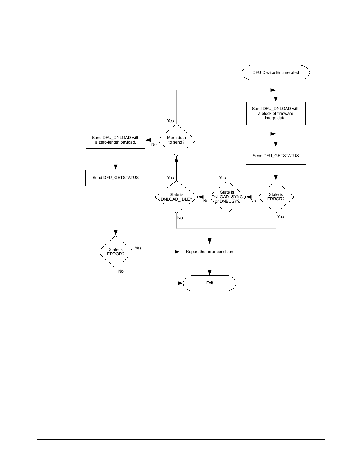
DFU Device Enumerated
Exit
Send DFU_GETSTATUS
No
Send DFU_DNLOAD with
a block of firmware
image data.
State is
ERROR?
Yes
State is
DNLOAD_SYNC
or DNBUSY?
State is
DNLOAD_IDLE?
More data
to send?
No
No
YesYes
Send DFU_DNLOAD with
a zero-length payload.
Report the error condition
Send DFU_GETSTATUS
Yes
No
State is
ERROR?
Yes
No
Boot Loader
April 8, 2013 15
Page 16

Boot Loader
2.3.4 Tiva-Specific USB Download Commands
The DFU class specification provides the framework necessary to download and upload firmware
files to the USB device but does not specify the actual format of the binary data that is transferred.
As a result, different device implementations have used different methods to perform operations
that are not defined in the standard such as:
Setting the address to flash a downloaded binary.
Setting the address and size of the area of flash with contents to be uploaded.
Erasing sections of the flash.
Querying the size of flash and writeable area addresses.
The USB boot loader implementation employs a small set of commands which can be sent to the
DFU device via a DFU_DNLOAD request when the device is in IDLE state. Each command takes
the form of an 8-byte structure that defines the operation to carry out and provides any required
additional parameters.
To ensure that a host application that does not have explicit support for Tiva-specific commands can
still be used to download binary firmware images to the device, the protocol is defined such that only
a single 8-byte header structure must be placed at the start of the binary image being downloaded.
This header and the DFU-defined suffix structure can both be added using the “dfuwrap” commandline application supplied with TivaWare, thus providing a single binary that can be sent to a device
running the Tiva USB boot loader using a standard sequence of DFU_DNLOAD requests with no
other embedded commands or device-specific operations required. An application which does
understand the Tiva-specific commands may make use of them to offer additional functionality that
would not otherwise be available.
Querying Command Support
Because the device-specific commands defined here are sent to the DFU device in DFU_DNLOAD
requests, the possibility exists that sending them to a device which does not understand the protocol
could result in corruption of that device’s firmware. To guard against this possibility, the USB boot
loader supports an additional USB request which is used to query the device capabilities and allow
a host to determine whether or not the device supports the Tiva commands. A device which does
not support the commands either stalls the request or returns unexpected data.
To determine whether a target DFU device supports the Tiva-specific DFU commands, send the
following IN request to the DFU interface:
bmRequestType
10100001b 0x42 0x23 Interface 4 Protocol Info
where the protocol information returned is a 4-byte structure, the first two bytes of which are 0x4D,
0x4C and the second two bytes indicates the protocol version supported, currently 0x01 and 0x00
respectively.
bRequest wValue wIndex wLength Data
Download Command Definitions
The following commands may be sent to the USB boot loader as the first 8 bytes of the payload to
a DFU_DNLOAD request. The boot loader expects any DFU_DNLOAD request received while in the
16 April 8, 2013
Page 17

Boot Loader
IDLE state to contain a command header but does not look for a command unless the state is IDLE.
This protocol allows an application that is unaware of the command header to download a DFUwrapped binary image using a standard sequence of multiple DFU_DNLOAD and DFU_GETSTATUS
requests without the need to insert additional command headers during the download.
The commands defined here and their parameter block structures can be found in header file
usbdfu.h provided with TivaWare. In all cases where multi-byte numbers are specified, the numbers are stored in little-endian format with the least significant byte in the lowest addressed location.
The following definitions specify the command byte ordering unambiguously but care must be taken
to ensure correct byte swapping if using the command structure types defined in usbdfu.h on bigendian systems.
DFU_CMD_PROG This command is used to provide the USB boot loader with the address at which
the next download should be written and the total length of the firmware image
that follows. This structure forms the header that is written to the DFU-wrapped
file generated by the dfuwrap tool.
The start address is provided in terms of 1024-byte flash blocks. To convert a
byte address to a block address, merely divide by 1024. The start address must
always be on a 1024-byte boundary.
This command may be followed by up to 1016 bytes of firmware image data,
this number being the maximum transfer size minus the 8 bytes of the command
structure.
The format of the command is as follows:
uint8_t pui8Data[8];
pui8Data[0] = DFU_CMD_PROG (0x01)
pui8Data[1] = Reserved - set to 0x00
pui8Data[2] = Start Block Number [7:0];
pui8Data[3] = Start Block Number [15:8];
pui8Data[4] = Image Size [7:0];
pui8Data[5] = Image Size [15:8];
pui8Data[6] = Image Size [23:16];
pui8Data[7] = Image Size [31:24];
April 8, 2013 17
Page 18

Boot Loader
DFU_CMD_READ This command is used to set the address range of the content to be returned
on subsequent DFU_UPLOAD requests from the host.
The start address is provided in terms of 1024-byte flash blocks. To convert a
byte address to a block address, divide by 1024. The start address must always
be on a 1024-byte boundary.
To read back a the contents of a region of flash, the host should send a
DFU_DNLOAD request with command DFU_CMD_READ, start address set to the
1KB block start address and length set to the number of bytes to read. The
host should then send one or more DFU_UPLOAD requests to receive the current flash contents from the configured addresses. Data returned includes an
8-byte DFU_CMD_PROG prefix structure unless the prefix has been disabled by
sending a DFU_CMD_BIN command with the bBinary parameter set to 1. The
host should, therefore, be prepared to read 8 bytes more than the length specified in the READ command if the prefix is enabled.
By default, the 8-byte prefix is enabled for all upload operations. This prefix
is required by the DFU class specification which states that uploaded images
must be formatted to allow them to be directly downloaded back to the device
at a later time.
The format of the command is as follows:
uint8_t pui8Data[8];
pui8Data[0] = DFU_CMD_READ (0x02)
pui8Data[1] = Reserved - set to 0x00
pui8Data[2] = Start Block Number [7:0];
pui8Data[3] = Start Block Number [15:8];
pui8Data[4] = Image Size [7:0];
pui8Data[5] = Image Size [15:8];
pui8Data[6] = Image Size [23:16];
pui8Data[7] = Image Size [31:24];
18 April 8, 2013
Page 19

Boot Loader
DFU_CMD_CHECK This command is used to check a region of flash to ensure that it is completely
erased.
The start address is provided in terms of 1024-byte flash blocks. To convert a
byte address to a block address, divide by 1024. The start address must always
be on a 1024-byte boundary. The length must also be a multiple of 4.
To check that a region of flash is erased, the DFU_CMD_CHECK command
should be sent with the required start address and region length set then the
host should issue a DFU_GETSTATUS request. If the erase check was successful, the returned bStatus value is OK (0x00), otherwise it is errCheckErased
(0x05).
The format of the command is as follows:
uint8_t pui8Data[8];
pui8Data[0] = DFU_CMD_CHECK (0x03)
pui8Data[1] = Reserved - set to 0x00
pui8Data[2] = Start Block Number [7:0];
pui8Data[3] = Start Block Number [15:8];
pui8Data[4] = Region Size [7:0];
pui8Data[5] = Region Size [15:8];
pui8Data[6] = Region Size [23:16];
pui8Data[7] = Region Size [31:24];
DFU_CMD_ERASE This command is used to erase a region of flash.
The start address is provided in terms of 1024-byte flash blocks. To convert a
byte address to a block address, divide by 1024. The start address must always
be on a 1024-byte boundary. The length must also be a multiple of 4.
The size of the region to erase is expressed in terms of flash blocks. The block
size can be determined using the DFU_CMD_INFO command.
The format of the command is as follows:
uint8_t pui8Data[8];
pui8Data[0] = DFU_CMD_ERASE (0x04)
pui8Data[1] = Reserved - set to 0x00
pui8Data[2] = Start Block Number [7:0];
pui8Data[3] = Start Block Number [15:8];
pui8Data[4] = Number of Blocks [7:0];
pui8Data[5] = Number of Blocks [15:8];
pui8Data[6] = Reserved - set to 0x00
pui8Data[7] = Reserved - set to 0x00
April 8, 2013 19
Page 20

Boot Loader
DFU_CMD_INFO This command is used to query information relating to the target de-
vice and programmable region of flash. The device information structure,
tDFUDeviceInfo, is returned on the next DFU_UPLOAD request following this
command.
The format of the command is as follows:
uint8_t pui8Data[8];
pui8Data[0] = DFU_CMD_INFO (0x05)
pui8Data[1] = Reserved - set to 0x00
pui8Data[2] = Reserved - set to 0x00
pui8Data[3] = Reserved - set to 0x00
pui8Data[4] = Reserved - set to 0x00
pui8Data[5] = Reserved - set to 0x00
pui8Data[6] = Reserved - set to 0x00
pui8Data[7] = Reserved - set to 0x00
//
*******************************************************************
//
// Payload returned in response to the DFU_CMD_INFO command.
//
// This is structure is returned in response to the first DFU_UPLOAD
// request following a DFU_CMD_INFO command. Note that byte ordering
// of multi-byte fields is little-endian.
//
//
*******************************************************************
typedef struct
{
//
// The size of a flash block in bytes.
//
uint16_t ui16FlashBlockSize;
//
// The number of blocks of flash in the device. Total
// flash size is usNumFlashBlocks*usFlashBlockSize.
//
uint16_t ui16NumFlashBlocks;
//
// Information on the part number, family, version and
// package as read from SYSCTL register DID1.
//
uint32_t ui32PartInfo;
//
// Information on the part class and revision as read
// from SYSCTL DID0.
//
uint32_t ui32ClassInfo;
//
// Address 1 byte above the highest location the boot
// loader can access.
//
uint32_t ui32FlashTop;
//
// Lowest address the boot loader can write or erase.
//
uint32_t ui32AppStartAddr;
}
PACKED tDFUDeviceInfo;
20 April 8, 2013
Page 21

Boot Loader
DFU_CMD_BIN By default, data returned in response to a DFU_UPLOAD request includes an
8-byte DFU_CMD_PROG prefix structure. This ensures that an uploaded image
can be directly downloaded again without the need to further wrap it but, in
cases where pure binary data is required, can be awkward. The DFU_CMD_BIN
command allows the upload prefix to be disabled or enabled under host control.
The format of the command is as follows:
uint8_t pui8Data[8];
pui8Data[0] = DFU_CMD_BIN (0x06)
pui8Data[1] = 0x01 to disable upload prefix, 0x00 to enable
pui8Data[2] = Reserved - set to 0x00
pui8Data[3] = Reserved - set to 0x00
pui8Data[4] = Reserved - set to 0x00
pui8Data[5] = Reserved - set to 0x00
pui8Data[6] = Reserved - set to 0x00
pui8Data[7] = Reserved - set to 0x00
DFU_CMD_RESET This command may be sent to the USB boot loader to cause it to perform a
soft reset of the board. This reboots the system and, assuming that the main
application image is present, runs the main application. Note that a reboot also
takes place if a firmware download operation completes and the host issues a
USB reset to the DFU device.
The format of the command is as follows:
uint8_t pui8Data[8];
pui8Data[0] = DFU_CMD_RESET (0x07)
pui8Data[1] = Reserved - set to 0x00
pui8Data[2] = Reserved - set to 0x00
pui8Data[3] = Reserved - set to 0x00
pui8Data[4] = Reserved - set to 0x00
pui8Data[5] = Reserved - set to 0x00
pui8Data[6] = Reserved - set to 0x00
pui8Data[7] = Reserved - set to 0x00
2.3.5 Customizing the USB Device Firmware Upgrade
The USB boot loader provides a method to pass a set of custom values to the boot loader when
called from a running application. When the USB boot loader is entered because the flash was
empty, the boot ROM offers no customization and provides generic “Texas Instruments” and “Device
Firmware Update” strings to the host as identifiers. The USB boot loader is called by an application
via a call to ROM_UpdateUSB(), which takes a single pointer as an argument that is a pointer to
an array containing the values that the boot loader uses for customization. This pointer can also be
0 to indicate that the application wishes to use the defaults provided by the ROM boot loader. The
application can place the customization structure anywhere in flash or SRAM.
April 8, 2013 21
Page 22

Boot Loader
The actual values that can be customized are the following:
Vendor ID (default 0x1CBE)
Product ID (default 0x00FF)
Bus/Self Power (default Self Powered)
Max Power (default 0)
Device Version (default 0x110)
All strings in multiple languages
The defaults for the strings are a Manufacturer set to “Texas Instruments”, Product set to “Device
Firmware Update”, and serial number set to “1.0”.
If the application is providing a structure to the boot loader with custom values, then the first 12
bytes must contain valid data. The values in the structure that is passed to the boot loader have the
following meaning and are merged directly to the device and configuration descriptor for the boot
loader:
Byte Value
0 VID bits 7:0
1 VID bits 15:8
2 PID bits 7:9
3 PID bits 15:8
4 Device Version(BCD) bits 7:9
5 Device Version(BCD) bits 15:8
6 Power in 2mA Increments(250 maximum)
7 USB Configuration Descriptor bmAttributes (Self powered 0xC0,
Bus powered 0x80).
8-11 Pointer to the string table
The values for the custom strings are contained in a pointer at the end of the structure passed to
the boot loader. If the application wants to use the default strings, this pointer should be set to 0.
The string table provided supports custom strings for Manufacturer, Product, and Serial Number in
multiple languages. The string table is optimized to not require that a string be provided for every
language in case there is not a unique string for every language. This is most likely the case for the
Serial Number string but it could be any string that is provided.
The string table has a header that describes the number of languages provided and the language
identifiers for each followed by a set of strings for each language. Each entry in the table has a size
header that specifies the size of the string in bytes plus a byte for the size itself and a one byte tag
of USB_DTYPE_STRING(0x03). This size and ID padding is included for ease of string handling in
the boot loader and is required. It is very important for the application to provide the correct size
values because the boot loader uses these to skip through the array and find the requested strings
requested by the USB host. If these sizes are incorrect, the boot loader may fail to enumerate, so
care should be taken when building the string table. The application must provide all three strings
in the first language because these strings are treated as the default if a string is left blank in
other languages. In other languages, a string can be left blank for strings that do not change per
language. A blank entry in the table consists of a two byte entry with a byte size value of 2 followed
by the USB_DTYPE_STRING value.
The string table has the following format:
22 April 8, 2013
Page 23

Byte Description
0 Size of the header(Number of Languages * 2) + 2
1 USB_DTYPE_STRING
2 Language ID 0 bits[7:0]
3 Language ID 0 bits[15:8]
... ...
. Language ID n bits[7:0]
. Language ID n bits[15:8]
. Language 0 Manufacturer string size in bytes + 2
. USB_DTYPE_STRING
. Language 0 Manufacturer Unicode String
. Language 0 Product string size in bytes + 2
. USB_DTYPE_STRING
. Language 0 Product Unicode String
. Language 0 Serial Number size in bytes + 2
. USB_DTYPE_STRING
. Language 0 Serial Number Unicode String
... ...
. Language n Manufacturer string size in bytes + 2
. USB_DTYPE_STRING
. Language n Manufacturer Unicode String
. Language n Product string size in bytes + 2
. USB_DTYPE_STRING
. Language n Product Unicode String
. Language n Serial Number size in bytes + 2
. USB_DTYPE_STRING
. Language n Serial Number Unicode String
Boot Loader
The next three examples show an example customization structure for a no string case, a single
language case and a multiple language case.
Example: No strings but custom descriptor.
uint8_t pui8USBBootROMInfo[] =
{
0xbe, 0x1c, // TI VID
0xff, 0x00, // Tiva DFU PID
0x00, 0x02, // USB version 2.0
0x00, // 0mA of Bus power
0xC0, // Self powered using no bus power
0 // Address of the string table
}
//
// Call to ROM USB boot loader.
//
ROM_UpdateUSB(pui8USBBootROMInfo);
Example: Single US English string set.
April 8, 2013 23
Page 24

Boot Loader
uint8_t pui8Strings[] =
{
(1*2) + 2, // One Language (1*2) + 2
USB_DTYPE_STRING,
0x09, 0x04, // Language code for US English.
(17*2) + 2, // Size of Manufacturer String.
// "Texas Instruments"
USB_DTYPE_STRING,
’T’, 0, ’e’, 0, ’x’, 0, ’a’, 0, ’s’, 0, ’ ’, 0, ’I’, 0, ’n’, 0,
’s’, 0, ’t’, 0, ’r’, 0, ’u’, 0, ’m’, 0, ’e’, 0, ’n’, 0, ’t’, 0,
’s’, 0,
(23*2) + 2, // Size of Product String.
USB_DTYPE_STRING,
// "Device Firmware Upgrade"
’D’, 0, ’e’, 0, ’v’, 0, ’i’, 0, ’c’, 0, ’e’, 0, ’ ’, 0, ’F’, 0,
’i’, 0, ’r’, 0, ’m’, 0, ’w’, 0, ’a’, 0, ’r’, 0, ’e’, 0, ’ ’, 0,
’U’, 0, ’p’, 0, ’g’, 0, ’r’, 0, ’a’, 0, ’d’, 0, ’e’, 0,
(3*2) + 2, // Size of Serial Number.
USB_DTYPE_STRING,
// "1.0"
’1’, 0, ’.’, 0, ’0’, 0
};
uint8_t pui8USBBootROMInfo[] =
{
0xbe, 0x1c, // TI VID
0xff, 0x00, // Tiva DFU PID
0x00, 0x02, // USB version 2.0
0x00, // 0mA of Bus power
0xC0, // Self powered using no bus power
pui8Strings // Address of the string table
}
//
// Call to ROM USB boot loader.
//
ROM_UpdateUSB(pui8USBBootROMInfo);
Example: Two Languages with English(United States) and Spanish(Mexico) strings.
uint8_t pui8Strings[] =
{
(2*2) + 2, // Two languages
USB_DTYPE_STRING,
0x09, 0x04, // Language code for English(United States).
0x0a, 0x08, // Language code for Spanish(Mexico)
(10*2) + 2, // Size of Manufacturer String.
24 April 8, 2013
Page 25

Boot Loader
// "My Company"
USB_DTYPE_STRING,
’M’, 0, ’y’, 0, ’ ’, 0, ’C’, 0, ’o’, 0, ’m’, 0, ’p’, 0, ’a’, 0,
’n’, 0, ’y’, 0
(23*2) + 2, // Size of Product String.
USB_DTYPE_STRING,
// "Device Firmware Upgrade"
’D’, 0, ’e’, 0, ’v’, 0, ’i’, 0, ’c’, 0, ’e’, 0, ’ ’, 0, ’F’, 0,
’i’, 0, ’r’, 0, ’m’, 0, ’w’, 0, ’a’, 0, ’r’, 0, ’e’, 0, ’ ’, 0,
’U’, 0, ’p’, 0, ’g’, 0, ’r’, 0, ’a’, 0, ’d’, 0, ’e’, 0,
(4*2) + 2, // Size of Serial Number.
USB_DTYPE_STRING,
// "1.01"
’1’, 0, ’.’, 0, ’0’, 0, ’1’, 0
(10*2) + 2, // Size of Manufacturer String.
USB_DTYPE_STRING,
// "My Company"
’M’, 0, ’y’, 0, ’ ’, 0, ’C’, 0, ’o’, 0, ’m’, 0, ’p’, 0, ’a’, 0,
’n’, 0, ’y’, 0
’s’, 0,
(25*2) + 2, // Size of Product String.
USB_DTYPE_STRING,
// "Actualizacion de Firmware"
’A’, 0, ’c’, 0, ’t’, 0, ’u’, 0, ’a’, 0, ’l’, 0, ’i’, 0, ’z’, 0,
’a’, 0, ’c’, 0, ’i’, 0, ’o’, 0, ’n’, 0, ’ ’, 0, ’d’, 0, ’e’, 0,
’ ’, 0, ’F’, 0, ’i’, 0, ’r’, 0, ’m’, 0, ’w’, 0, ’a’, 0, ’r’, 0,
’e’, 0,
2, // Size of Serial Number, this will use the last
// serial number found since this represents a null
// string.
USB_DTYPE_STRING,
};
uint8_t pui8USBBootROMInfo[] =
{
0xbe, 0x1c, // TI VID
0xff, 0x00, // Tiva DFU PID
250, // 500mA of Bus power
0x80, // Bus Powered
0x00, 0x02, // USB version 2.0
pui8Strings // Address of the string table
};
//
// Call to ROM USB boot loader.
//
ROM_UpdateUSB(pui8USBBootROMInfo);
April 8, 2013 25
Page 26

Boot Loader
26 April 8, 2013
Page 27

3 AES Data Tables
Introduction . . .. . . . . . .. . . . . . .. . . . . . .. . . . . . .. . . . . . .. . . . .. . . .. . .. . . . .. . . . . . .. . . . . . .. . . . . . .. . . . . . .. . . . .. . . . . . 27
Functions . . .. . . . .. . . .. . .. . . . .. . . . . . .. . . . . . .. . . . . . .. . . . . . .. . . . .. . . .. . .. . . . .. . . . . . .. . . . . . .. . . . .. . . .. . .. . . . .27
3.1 Introduction
The Advanced Encryption Standard (AES) is a publicly defined encryption standard used by the
U.S. Government. It is a strong encryption method with reasonable performance and size. AES
is fast in both hardware and software, is fairly easy to implement, and requires little memory. AES
is ideal for applications that can use pre-arranged keys, such as setup during manufacturing or
configuration.
Four data tables used by the XySSL AES implementation are provided in the ROM. The first is
the forward S-box substitution table, the second is the reverse S-box substitution table, the third is
the forward polynomial table, and the final is the reverse polynomial table. The meanings of these
tables and their use can be found in the AES code provided in TivaWare.
AES Data Tables
3.2 Data Structures
Data Structures
ROM_pvAESTable
3.2.1 Data Structure Documentation
3.2.1.1 ROM_pvAESTable
This structure describes the AES tables that are available in the ROM.
ROM Location:
ROM_APITABLE is an array of pointers located at 0x0100.0010.
ROM_SOFTWARETABLE is an array of pointers located at ROM_APITABLE[21].
ROM_pvAESTable is an array located at &ROM_SOFTWARETABLE[7].
Definition:
typedef struct
{
unsigned char ucForwardSBox[256];
unsigned long ulForwardTable[256];
unsigned char ucReverseSBox[256];
unsigned long ulReverseTable[256];
}
ROM_pvAESTable
Members:
ucForwardSBox This table contains the forward S-Box, as defined by the AES standard.
April 8, 2013 27
Page 28

AES Data Tables
ulForwardTable This table contains the forward polynomial table, as used by the XySSL AES
implementation.
ucReverseSBox This table contains the reverse S-Box, as defined by the AES standard. This
is simply the reverse of ucForwardSBox.
ulReverseTable This table contains the reverse polynomial table, as used by the XySSL AES
implementation.
28 April 8, 2013
Page 29

4 Analog Comparator
Introduction . . .. . . . . . .. . . . . . .. . . . . . .. . . . . . .. . . . . . .. . . . .. . . .. . .. . . . .. . . . . . .. . . . . . .. . . . . . .. . . . . . .. . . . .. . . . . . 29
Functions . . .. . . . .. . . .. . .. . . . .. . . . . . .. . . . . . .. . . . . . .. . . . . . .. . . . .. . . .. . .. . . . .. . . . . . .. . . . . . .. . . . .. . . .. . .. . . . .29
4.1 Introduction
The comparator API provides a set of functions for dealing with the analog comparators. A comparator can compare a test voltage against individual external reference voltage, a shared single
external reference voltage, or a shared internal reference voltage. It can provide its output to a
device pin, acting as a replacement for an analog comparator on the board, or it can be used to
signal the application via interrupts or triggers to the ADC to cause it to start capturing a sample
sequence. The interrupt generation and ADC triggering logic is separate, so that an interrupt can
be generated on a rising edge and the ADC triggered on a falling edge (for example).
4.2 Functions
Analog Comparator
Functions
void ROM_ComparatorConfigure (uint32_t ui32Base, uint32_t ui32Comp, uint32_t ui32Config)
void ROM_ComparatorIntClear (uint32_t ui32Base, uint32_t ui32Comp)
void ROM_ComparatorIntDisable (uint32_t ui32Base, uint32_t ui32Comp)
void ROM_ComparatorIntEnable (uint32_t ui32Base, uint32_t ui32Comp)
bool ROM_ComparatorIntStatus (uint32_t ui32Base, uint32_t ui32Comp, bool bMasked)
void ROM_ComparatorRefSet (uint32_t ui32Base, uint32_t ui32Ref)
bool ROM_ComparatorValueGet (uint32_t ui32Base, uint32_t ui32Comp)
4.2.1 Function Documentation
4.2.1.1 ROM_ComparatorConfigure
Configures a comparator.
Prototype:
void
ROM_ComparatorConfigure(uint32_t ui32Base,
uint32_t ui32Comp,
uint32_t ui32Config)
ROM Location:
ROM_APITABLE is an array of pointers located at 0x0100.0010.
ROM_COMPARATORTABLE is an array of pointers located at ROM_APITABLE[6].
ROM_ComparatorConfigure is a function pointer located at ROM_COMPARATORTABLE[1].
April 8, 2013 29
Page 30

Analog Comparator
Parameters:
Description:
ui32Base is the base address of the comparator module.
ui32Comp is the index of the comparator to configure.
ui32Config is the configuration of the comparator.
This function configures a comparator. The ui32Config parameter is the result of a logical
OR operation between the COMP_TRIG_xxx, COMP_INT_xxx, COMP_ASRCP_xxx, and
COMP_OUTPUT_xxx values.
The COMP_TRIG_xxx term can take on the following values:
COMP_TRIG_NONE to have no trigger to the ADC.
COMP_TRIG_HIGH to trigger the ADC when the comparator output is high.
COMP_TRIG_LOW to trigger the ADC when the comparator output is low.
COMP_TRIG_FALL to trigger the ADC when the comparator output goes low.
COMP_TRIG_RISE to trigger the ADC when the comparator output goes high.
COMP_TRIG_BOTH to trigger the ADC when the comparator output goes low or high.
The COMP_INT_xxx term can take on the following values:
COMP_INT_HIGH to generate an interrupt when the comparator output is high.
COMP_INT_LOW to generate an interrupt when the comparator output is low.
COMP_INT_FALL to generate an interrupt when the comparator output goes low.
COMP_INT_RISE to generate an interrupt when the comparator output goes high.
COMP_INT_BOTH to generate an interrupt when the comparator output goes low or high.
The COMP_ASRCP_xxx term can take on the following values:
COMP_ASRCP_PIN to use the dedicated Comp+ pin as the reference voltage.
COMP_ASRCP_PIN0 to use the Comp0+ pin as the reference voltage (this the same as
COMP_ASRCP_PIN for the comparator 0).
COMP_ASRCP_REF to use the internally generated voltage as the reference voltage.
The COMP_OUTPUT_xxx term can take on the following values:
COMP_OUTPUT_NORMAL to enable a non-inverted output from the comparator to a
device pin.
COMP_OUTPUT_INVERT to enable an inverted output from the comparator to a device
pin.
Returns:
None.
4.2.1.2 ROM_ComparatorIntClear
Clears a comparator interrupt.
Prototype:
void
ROM_ComparatorIntClear(uint32_t ui32Base,
uint32_t ui32Comp)
30 April 8, 2013
Page 31

Analog Comparator
ROM Location:
ROM_APITABLE is an array of pointers located at 0x0100.0010.
ROM_COMPARATORTABLE is an array of pointers located at ROM_APITABLE[6].
ROM_ComparatorIntClear is a function pointer located at ROM_COMPARATORTABLE[0].
Parameters:
ui32Base is the base address of the comparator module.
ui32Comp is the index of the comparator.
Description:
The comparator interrupt is cleared, so that it no longer asserts. This function must be called in
the interrupt handler to keep the handler from being called again immediately upon exit. Note
that for a level-triggered interrupt, the interrupt cannot be cleared until it stops asserting.
Note:
Because there is a write buffer in the Cortex-M4 processor, it may take several clock cycles
before the interrupt source is actually cleared. Therefore, it is recommended that the interrupt
source be cleared early in the interrupt handler (as opposed to the very last action) to avoid
returning from the interrupt handler before the interrupt source is actually cleared. Failure to
do so may result in the interrupt handler being immediately reentered (because the interrupt
controller still sees the interrupt source asserted).
Returns:
None.
4.2.1.3 ROM_ComparatorIntDisable
Disables the comparator interrupt.
Prototype:
void
ROM_ComparatorIntDisable(uint32_t ui32Base,
ROM Location:
ROM_APITABLE is an array of pointers located at 0x0100.0010.
ROM_COMPARATORTABLE is an array of pointers located at ROM_APITABLE[6].
ROM_ComparatorIntDisable is a function pointer located at ROM_COMPARATORTABLE[5].
Parameters:
ui32Base is the base address of the comparator module.
ui32Comp is the index of the comparator.
Description:
This function disables generation of an interrupt from the specified comparator. Only comparators whose interrupts are enabled can be reflected to the processor.
Returns:
None.
uint32_t ui32Comp)
April 8, 2013 31
Page 32

Analog Comparator
4.2.1.4 ROM_ComparatorIntEnable
Enables the comparator interrupt.
Prototype:
void
ROM_ComparatorIntEnable(uint32_t ui32Base,
ROM Location:
ROM_APITABLE is an array of pointers located at 0x0100.0010.
ROM_COMPARATORTABLE is an array of pointers located at ROM_APITABLE[6].
ROM_ComparatorIntEnable is a function pointer located at ROM_COMPARATORTABLE[4].
Parameters:
ui32Base is the base address of the comparator module.
ui32Comp is the index of the comparator.
Description:
This function enables generation of an interrupt from the specified comparator. Only comparators whose interrupts are enabled can be reflected to the processor.
Returns:
None.
uint32_t ui32Comp)
4.2.1.5 ROM_ComparatorIntStatus
Gets the current interrupt status.
Prototype:
bool
ROM_ComparatorIntStatus(uint32_t ui32Base,
ROM Location:
ROM_APITABLE is an array of pointers located at 0x0100.0010.
ROM_COMPARATORTABLE is an array of pointers located at ROM_APITABLE[6].
ROM_ComparatorIntStatus is a function pointer located at ROM_COMPARATORTABLE[6].
Parameters:
ui32Base is the base address of the comparator module.
ui32Comp is the index of the comparator.
bMasked is false if the raw interrupt status is required and true if the masked interrupt status
is required.
Description:
This returns the interrupt status for the comparator. Either the raw or the masked interrupt
status can be returned.
uint32_t ui32Comp,
bool bMasked)
Returns:
true if the interrupt is asserted and false if it is not asserted.
32 April 8, 2013
Page 33

4.2.1.6 ROM_ComparatorRefSet
Sets the internal reference voltage.
Prototype:
void
ROM_ComparatorRefSet(uint32_t ui32Base,
ROM Location:
ROM_APITABLE is an array of pointers located at 0x0100.0010.
ROM_COMPARATORTABLE is an array of pointers located at ROM_APITABLE[6].
ROM_ComparatorRefSet is a function pointer located at ROM_COMPARATORTABLE[2].
Parameters:
ui32Base is the base address of the comparator module.
ui32Ref is the desired reference voltage.
Description:
This function sets the internal reference voltage value. The voltage is specified as one of the
following values:
COMP_REF_OFF to turn off the reference voltage
COMP_REF_0V to set the reference voltage to 0 V
COMP_REF_0_1375V to set the reference voltage to 0.1375 V
COMP_REF_0_275V to set the reference voltage to 0.275 V
COMP_REF_0_4125V to set the reference voltage to 0.4125 V
COMP_REF_0_55V to set the reference voltage to 0.55 V
COMP_REF_0_6875V to set the reference voltage to 0.6875 V
COMP_REF_0_825V to set the reference voltage to 0.825 V
COMP_REF_0_928125V to set the reference voltage to 0.928125 V
COMP_REF_0_9625V to set the reference voltage to 0.9625 V
COMP_REF_1_03125V to set the reference voltage to 1.03125 V
COMP_REF_1_134375V to set the reference voltage to 1.134375 V
COMP_REF_1_1V to set the reference voltage to 1.1 V
COMP_REF_1_2375V to set the reference voltage to 1.2375 V
COMP_REF_1_340625V to set the reference voltage to 1.340625 V
COMP_REF_1_375V to set the reference voltage to 1.375 V
COMP_REF_1_44375V to set the reference voltage to 1.44375 V
COMP_REF_1_5125V to set the reference voltage to 1.5125 V
COMP_REF_1_546875V to set the reference voltage to 1.546875 V
COMP_REF_1_65V to set the reference voltage to 1.65 V
COMP_REF_1_753125V to set the reference voltage to 1.753125 V
COMP_REF_1_7875V to set the reference voltage to 1.7875 V
COMP_REF_1_85625V to set the reference voltage to 1.85625 V
COMP_REF_1_925V to set the reference voltage to 1.925 V
COMP_REF_1_959375V to set the reference voltage to 1.959375 V
COMP_REF_2_0625V to set the reference voltage to 2.0625 V
COMP_REF_2_165625V to set the reference voltage to 2.165625 V
Analog Comparator
uint32_t ui32Ref)
April 8, 2013 33
Page 34

Analog Comparator
COMP_REF_2_26875V to set the reference voltage to 2.26875 V
COMP_REF_2_371875V to set the reference voltage to 2.371875 V
Returns:
None.
4.2.1.7 ROM_ComparatorValueGet
Gets the current comparator output value.
Prototype:
bool
ROM_ComparatorValueGet(uint32_t ui32Base,
ROM Location:
ROM_APITABLE is an array of pointers located at 0x0100.0010.
ROM_COMPARATORTABLE is an array of pointers located at ROM_APITABLE[6].
ROM_ComparatorValueGet is a function pointer located at ROM_COMPARATORTABLE[3].
Parameters:
ui32Base is the base address of the comparator module.
ui32Comp is the index of the comparator.
uint32_t ui32Comp)
Description:
This function retrieves the current value of the comparator output.
Returns:
Returns true if the comparator output is high and false if the comparator output is low.
34 April 8, 2013
Page 35

Analog to Digital Converter (ADC)
5 Analog to Digital Converter (ADC)
Introduction . . .. . . . . . .. . . . . . .. . . . . . .. . . . . . .. . . . . . .. . . . .. . . .. . .. . . . .. . . . . . .. . . . . . .. . . . . . .. . . . . . .. . . . .. . . . . . 35
Functions . . .. . . . .. . . .. . .. . . . .. . . . . . .. . . . . . .. . . . . . .. . . . . . .. . . . .. . . .. . .. . . . .. . . . . . .. . . . . . .. . . . .. . . .. . .. . . . .35
5.1 Introduction
The analog to digital converter (ADC) API provides a set of functions for dealing with the ADC.
Functions are provided to configure the sample sequencers, read the captured data, register a
sample sequence interrupt handler, and handle interrupt masking/clearing.
The ADC supports twelve input channels plus an internal temperature sensor. Four sampling sequences, each with configurable trigger events, can be captured. The first sequence will capture up
to eight samples, the second and third sequences will capture up to four samples, and the fourth
sequence will capture a single sample. Each sample can be the same channel, different channels,
or any combination in any order.
The sample sequences have configurable priorities that determine the order in which they are captured when multiple triggers occur simultaneously. The highest priority sequence that is currently
triggered will be sampled. Care must be taken with triggers that occur frequently (such as the
“always” trigger); if their priority is too high it is possible to starve the lower priority sequences.
Hardware oversampling of the ADC data is available for improved accuracy. An oversampling factor of 2x, 4x, 8x, 16x, 32x, and 64x is supported, but reduces the throughput of the ADC by a
corresponding factor. Hardware oversampling is applied uniformly across all sample sequences.
5.2 Functions
Functions
void ROM_ADCComparatorConfigure (uint32_t ui32Base, uint32_t ui32Comp, uint32_t
ui32Config)
void ROM_ADCComparatorIntClear (uint32_t ui32Base, uint32_t ui32Status)
void ROM_ADCComparatorIntDisable (uint32_t ui32Base, uint32_t ui32SequenceNum)
void ROM_ADCComparatorIntEnable (uint32_t ui32Base, uint32_t ui32SequenceNum)
uint32_t ROM_ADCComparatorIntStatus (uint32_t ui32Base)
void ROM_ADCComparatorRegionSet (uint32_t ui32Base, uint32_t ui32Comp, uint32_t
ui32LowRef, uint32_t ui32HighRef)
void ROM_ADCComparatorReset (uint32_t ui32Base, uint32_t ui32Comp, bool bTrigger, bool
bInterrupt)
void ROM_ADCHardwareOversampleConfigure (uint32_t ui32Base, uint32_t ui32Factor)
void ROM_ADCIntClear (uint32_t ui32Base, uint32_t ui32SequenceNum)
void ROM_ADCIntDisable (uint32_t ui32Base, uint32_t ui32SequenceNum)
void ROM_ADCIntEnable (uint32_t ui32Base, uint32_t ui32SequenceNum)
uint32_t ROM_ADCIntStatus (uint32_t ui32Base, uint32_t ui32SequenceNum, bool bMasked)
uint32_t ROM_ADCPhaseDelayGet (uint32_t ui32Base)
April 8, 2013 35
Page 36

Analog to Digital Converter (ADC)
void ROM_ADCPhaseDelaySet (uint32_t ui32Base, uint32_t ui32Phase)
void ROM_ADCProcessorTrigger (uint32_t ui32Base, uint32_t ui32SequenceNum)
uint32_t ROM_ADCReferenceGet (uint32_t ui32Base)
void ROM_ADCReferenceSet (uint32_t ui32Base, uint32_t ui32Ref)
void ROM_ADCSequenceConfigure (uint32_t ui32Base, uint32_t ui32SequenceNum, uint32_t
ui32Trigger, uint32_t ui32Priority)
int32_t ROM_ADCSequenceDataGet (uint32_t ui32Base, uint32_t ui32SequenceNum,
uint32_t ∗pui32Buffer)
void ROM_ADCSequenceDisable (uint32_t ui32Base, uint32_t ui32SequenceNum)
void ROM_ADCSequenceEnable (uint32_t ui32Base, uint32_t ui32SequenceNum)
int32_t ROM_ADCSequenceOverflow (uint32_t ui32Base, uint32_t ui32SequenceNum)
void ROM_ADCSequenceOverflowClear (uint32_t ui32Base, uint32_t ui32SequenceNum)
void ROM_ADCSequenceStepConfigure (uint32_t ui32Base, uint32_t ui32SequenceNum,
uint32_t ui32Step, uint32_t ui32Config)
int32_t ROM_ADCSequenceUnderflow (uint32_t ui32Base, uint32_t ui32SequenceNum)
void ROM_ADCSequenceUnderflowClear (uint32_t ui32Base, uint32_t ui32SequenceNum)
5.2.1 Function Documentation
5.2.1.1 ROM_ADCComparatorConfigure
Configures an ADC digital comparator.
Prototype:
void
ROM_ADCComparatorConfigure(uint32_t ui32Base,
ROM Location:
ROM_APITABLE is an array of pointers located at 0x0100.0010.
ROM_ADCTABLE is an array of pointers located at ROM_APITABLE[5].
ROM_ADCComparatorConfigure is a function pointer located at ROM_ADCTABLE[15].
Parameters:
ui32Base is the base address of the ADC module.
ui32Comp is the index of the comparator to configure.
ui32Config is the configuration of the comparator.
Description:
This function will configure a comparator. The ui32Config parameter is the result of a logical
OR operation between the ADC_COMP_TRIG_xxx, and ADC_COMP_INT_xxx values.
The ADC_COMP_TRIG_xxx term can take on the following values:
uint32_t ui32Comp,
uint32_t ui32Config)
ADC_COMP_TRIG_NONE to never trigger PWM fault condition.
ADC_COMP_TRIG_LOW_ALWAYS to always trigger PWM fault condition when ADC out-
put is in the low-band.
ADC_COMP_TRIG_LOW_ONCE to trigger PWM fault condition once when ADC output
transitions into the low-band.
36 April 8, 2013
Page 37

Analog to Digital Converter (ADC)
ADC_COMP_TRIG_LOW_HALWAYS to always trigger PWM fault condition when ADC
output is in the low-band only if ADC output has been in the high-band since the last
trigger output.
ADC_COMP_TRIG_LOW_HONCE to trigger PWM fault condition once when ADC output
transitions into low-band only if ADC output has been in the high-band since the last trigger
output.
ADC_COMP_TRIG_MID_ALWAYS to always trigger PWM fault condition when ADC output is in the mid-band.
ADC_COMP_TRIG_MID_ONCE to trigger PWM fault condition once when ADC output
transitions into the mid-band.
ADC_COMP_TRIG_HIGH_ALWAYS to always trigger PWM fault condition when ADC output is in the high-band.
ADC_COMP_TRIG_HIGH_ONCE to trigger PWM fault condition once when ADC output
transitions into the high-band.
ADC_COMP_TRIG_HIGH_HALWAYS to always trigger PWM fault condition when ADC
output is in the high-band only if ADC output has been in the low-band since the last
trigger output.
ADC_COMP_TRIG_HIGH_HONCE to trigger PWM fault condition once when ADC output
transitions into high-band only if ADC output has been in the low-band since the last trigger
output.
The ADC_COMP_INT_xxx term can take on the following values:
ADC_COMP_INT_NONE to never generate ADC interrupt.
ADC_COMP_INT_LOW_ALWAYS to always generate ADC interrupt when ADC output is
in the low-band.
ADC_COMP_INT_LOW_ONCE to generate ADC interrupt once when ADC output transi-
tions into the low-band.
ADC_COMP__INT_LOW_HALWAYS to always generate ADC interrupt when ADC output
is in the low-band only if ADC output has been in the high-band since the last trigger output.
ADC_COMP_INT_LOW_HONCE to generate ADC interrupt once when ADC output tran-
sitions into low-band only if ADC output has been in the high-band since the last trigger
output.
ADC_COMP_INT_MID_ALWAYS to always generate ADC interrupt when ADC output is
in the mid-band.
ADC_COMP_INT_MID_ONCE to generate ADC interrupt once when ADC output transitions into the mid-band.
ADC_COMP_INT_HIGH_ALWAYS to always generate ADC interrupt when ADC output is
in the high-band.
ADC_COMP_INT_HIGH_ONCE to generate ADC interrupt once when ADC output transitions into the high-band.
ADC_COMP_INT_HIGH_HALWAYS to always generate ADC interrupt when ADC output
is in the high-band only if ADC output has been in the low-band since the last trigger output.
ADC_COMP_INT_HIGH_HONCE to generate ADC interrupt once when ADC output transitions into high-band only if ADC output has been in the low-band since the last trigger
output.
Returns:
None.
April 8, 2013 37
Page 38

Analog to Digital Converter (ADC)
5.2.1.2 ROM_ADCComparatorIntClear
Clears sample sequence comparator interrupt source.
Prototype:
void
ROM_ADCComparatorIntClear(uint32_t ui32Base,
ROM Location:
ROM_APITABLE is an array of pointers located at 0x0100.0010.
ROM_ADCTABLE is an array of pointers located at ROM_APITABLE[5].
ROM_ADCComparatorIntClear is a function pointer located at ROM_ADCTABLE[21].
Parameters:
ui32Base is the base address of the ADC module.
ui32Status is the bit-mapped interrupts status to clear.
Description:
The specified interrupt status is cleared.
Returns:
None.
uint32_t ui32Status)
5.2.1.3 ROM_ADCComparatorIntDisable
Disables a sample sequence comparator interrupt.
Prototype:
void
ROM_ADCComparatorIntDisable(uint32_t ui32Base,
ROM Location:
ROM_APITABLE is an array of pointers located at 0x0100.0010.
ROM_ADCTABLE is an array of pointers located at ROM_APITABLE[5].
ROM_ADCComparatorIntDisable is a function pointer located at ROM_ADCTABLE[18].
Parameters:
ui32Base is the base address of the ADC module.
ui32SequenceNum is the sample sequence number.
Description:
This function disables the requested sample sequence comparator interrupt.
Returns:
None.
uint32_t ui32SequenceNum)
38 April 8, 2013
Page 39

5.2.1.4 ROM_ADCComparatorIntEnable
Enables a sample sequence comparator interrupt.
Prototype:
void
ROM_ADCComparatorIntEnable(uint32_t ui32Base,
ROM Location:
ROM_APITABLE is an array of pointers located at 0x0100.0010.
ROM_ADCTABLE is an array of pointers located at ROM_APITABLE[5].
ROM_ADCComparatorIntEnable is a function pointer located at ROM_ADCTABLE[19].
Parameters:
ui32Base is the base address of the ADC module.
ui32SequenceNum is the sample sequence number.
Description:
This function enables the requested sample sequence comparator interrupt.
Returns:
None.
Analog to Digital Converter (ADC)
uint32_t ui32SequenceNum)
5.2.1.5 ROM_ADCComparatorIntStatus
Gets the current comparator interrupt status.
Prototype:
uint32_t
ROM_ADCComparatorIntStatus(uint32_t ui32Base)
ROM Location:
ROM_APITABLE is an array of pointers located at 0x0100.0010.
ROM_ADCTABLE is an array of pointers located at ROM_APITABLE[5].
ROM_ADCComparatorIntStatus is a function pointer located at ROM_ADCTABLE[20].
Parameters:
ui32Base is the base address of the ADC module.
Description:
This returns the digitial comparator interrupt status bits. This status is sequence agnostic.
Returns:
The current comparator interrupt status.
5.2.1.6 ROM_ADCComparatorRegionSet
Defines the ADC digital comparator regions.
April 8, 2013 39
Page 40

Analog to Digital Converter (ADC)
Prototype:
void
ROM_ADCComparatorRegionSet(uint32_t ui32Base,
ROM Location:
ROM_APITABLE is an array of pointers located at 0x0100.0010.
ROM_ADCTABLE is an array of pointers located at ROM_APITABLE[5].
ROM_ADCComparatorRegionSet is a function pointer located at ROM_ADCTABLE[16].
Parameters:
ui32Base is the base address of the ADC module.
ui32Comp is the index of the comparator to configure.
ui32LowRef is the reference point for the low/mid band threshold.
ui32HighRef is the reference point for the mid/high band threshold.
Description:
The ADC digital comparator operation is based on three ADC value regions:
low-band is defined as any ADC value less than or equal to the ui32LowRef value.
mid-band is defined as any ADC value greater than the ui32LowRef value but less than
or equal to the ui32HighRef value.
high-band is defined as any ADC value greater than the ui32HighRef value.
uint32_t ui32Comp,
uint32_t ui32LowRef,
uint32_t ui32HighRef)
Returns:
None.
5.2.1.7 ROM_ADCComparatorReset
Resets the current ADC digital comparator conditions.
Prototype:
void
ROM_ADCComparatorReset(uint32_t ui32Base,
ROM Location:
ROM_APITABLE is an array of pointers located at 0x0100.0010.
ROM_ADCTABLE is an array of pointers located at ROM_APITABLE[5].
ROM_ADCComparatorReset is a function pointer located at ROM_ADCTABLE[17].
Parameters:
ui32Base is the base address of the ADC module.
ui32Comp is the index of the comparator.
bTrigger is the flag to indicate reset of Trigger conditions.
bInterrupt is the flag to indicate reset of Interrupt conditions.
uint32_t ui32Comp,
bool bTrigger,
bool bInterrupt)
40 April 8, 2013
Page 41

Description:
Because the digital comparator uses current and previous ADC values, this function is provide
to allow the comparator to be reset to its initial value to prevent stale data from being used
when a sequence is enabled.
Returns:
None.
5.2.1.8 ROM_ADCHardwareOversampleConfigure
Configures the hardware oversampling factor of the ADC.
Prototype:
void
ROM_ADCHardwareOversampleConfigure(uint32_t ui32Base,
ROM Location:
ROM_APITABLE is an array of pointers located at 0x0100.0010.
ROM_ADCTABLE is an array of pointers located at ROM_APITABLE[5].
ROM_ADCHardwareOversampleConfigure is a function pointer located at
ROM_ADCTABLE[14].
Analog to Digital Converter (ADC)
uint32_t ui32Factor)
Parameters:
ui32Base is the base address of the ADC module.
ui32Factor is the number of samples to be averaged.
Description:
This function configures the hardware oversampling for the ADC, which can be used to provide
better resolution on the sampled data. Oversampling is accomplished by averaging multiple
samples from the same analog input. Six different oversampling rates are supported; 2x,
4x, 8x, 16x, 32x, and 64x. Specifying an oversampling factor of zero will disable hardware
oversampling.
Hardware oversampling applies uniformly to all sample sequencers. It does not reduce the
depth of the sample sequencers like the software oversampling APIs; each sample written into
the sample sequence FIFO is a fully oversampled analog input reading.
Enabling hardware averaging increases the precision of the ADC at the cost of throughput. For
example, enabling 4x oversampling reduces the throughput of a 250 Ksps ADC to 62.5 Ksps.
Returns:
None.
5.2.1.9 ROM_ADCIntClear
Clears sample sequence interrupt source.
Prototype:
void
ROM_ADCIntClear(uint32_t ui32Base,
uint32_t ui32SequenceNum)
April 8, 2013 41
Page 42

Analog to Digital Converter (ADC)
ROM Location:
ROM_APITABLE is an array of pointers located at 0x0100.0010.
ROM_ADCTABLE is an array of pointers located at ROM_APITABLE[5].
ROM_ADCIntClear is a function pointer located at ROM_ADCTABLE[4].
Parameters:
ui32Base is the base address of the ADC module.
ui32SequenceNum is the sample sequence number.
Description:
The specified sample sequence interrupt is cleared, so that it no longer asserts. This must be
done in the interrupt handler to keep it from being called again immediately upon exit.
Note:
Because there is a write buffer in the Cortex-M4 processor, it may take several clock cycles
before the interrupt source is actually cleared. Therefore, it is recommended that the interrupt
source be cleared early in the interrupt handler (as opposed to the very last action) to avoid
returning from the interrupt handler before the interrupt source is actually cleared. Failure to
do so may result in the interrupt handler being immediately reentered (because the interrupt
controller still sees the interrupt source asserted).
Returns:
None.
5.2.1.10 ROM_ADCIntDisable
Disables a sample sequence interrupt.
Prototype:
void
ROM_ADCIntDisable(uint32_t ui32Base,
ROM Location:
ROM_APITABLE is an array of pointers located at 0x0100.0010.
ROM_ADCTABLE is an array of pointers located at ROM_APITABLE[5].
ROM_ADCIntDisable is a function pointer located at ROM_ADCTABLE[1].
Parameters:
ui32Base is the base address of the ADC module.
ui32SequenceNum is the sample sequence number.
Description:
This function disables the requested sample sequence interrupt.
Returns:
None.
uint32_t ui32SequenceNum)
5.2.1.11 ROM_ADCIntEnable
Enables a sample sequence interrupt.
42 April 8, 2013
Page 43

Analog to Digital Converter (ADC)
Prototype:
void
ROM_ADCIntEnable(uint32_t ui32Base,
uint32_t ui32SequenceNum)
ROM Location:
ROM_APITABLE is an array of pointers located at 0x0100.0010.
ROM_ADCTABLE is an array of pointers located at ROM_APITABLE[5].
ROM_ADCIntEnable is a function pointer located at ROM_ADCTABLE[2].
Parameters:
ui32Base is the base address of the ADC module.
ui32SequenceNum is the sample sequence number.
Description:
This function enables the requested sample sequence interrupt. Any outstanding interrupts
are cleared before enabling the sample sequence interrupt.
Returns:
None.
5.2.1.12 ROM_ADCIntStatus
Gets the current interrupt status.
Prototype:
uint32_t
ROM_ADCIntStatus(uint32_t ui32Base,
ROM Location:
ROM_APITABLE is an array of pointers located at 0x0100.0010.
ROM_ADCTABLE is an array of pointers located at ROM_APITABLE[5].
ROM_ADCIntStatus is a function pointer located at ROM_ADCTABLE[3].
Parameters:
ui32Base is the base address of the ADC module.
ui32SequenceNum is the sample sequence number.
bMasked is false if the raw interrupt status is required and true if the masked interrupt status
is required.
Description:
This returns the interrupt status for the specified sample sequence. Either the raw interrupt
status or the status of interrupts that are allowed to reflect to the processor can be returned.
uint32_t ui32SequenceNum,
bool bMasked)
Returns:
The current raw or masked interrupt status.
April 8, 2013 43
Page 44

Analog to Digital Converter (ADC)
5.2.1.13 ROM_ADCPhaseDelayGet
Gets the phase delay between a trigger and the start of a sequence.
Prototype:
uint32_t
ROM_ADCPhaseDelayGet(uint32_t ui32Base)
ROM Location:
ROM_APITABLE is an array of pointers located at 0x0100.0010.
ROM_ADCTABLE is an array of pointers located at ROM_APITABLE[5].
ROM_ADCPhaseDelayGet is a function pointer located at ROM_ADCTABLE[25].
Parameters:
ui32Base is the base address of the ADC module.
Description:
This function gets the current phase delay between the detection of an ADC trigger event and
the start of the sample sequence.
Returns:
Returns the phase delay, specified as one of ADC_PHASE_0, ADC_PHASE_22_5,
ADC_PHASE_45, ADC_PHASE_67_5, ADC_PHASE_90, ADC_PHASE_112_5,
ADC_PHASE_135, ADC_PHASE_157_5, ADC_PHASE_180, ADC_PHASE_202_5,
ADC_PHASE_225, ADC_PHASE_247_5, ADC_PHASE_270, ADC_PHASE_292_5,
ADC_PHASE_315, or ADC_PHASE_337_5.
5.2.1.14 ROM_ADCPhaseDelaySet
Sets the phase delay between a trigger and the start of a sequence.
Prototype:
void
ROM_ADCPhaseDelaySet(uint32_t ui32Base,
ROM Location:
ROM_APITABLE is an array of pointers located at 0x0100.0010.
ROM_ADCTABLE is an array of pointers located at ROM_APITABLE[5].
ROM_ADCPhaseDelaySet is a function pointer located at ROM_ADCTABLE[24].
Parameters:
ui32Base is the base address of the ADC module.
ui32Phase is the phase delay, specified as one of ADC_PHASE_0, ADC_PHASE_22_5,
ADC_PHASE_45, ADC_PHASE_67_5, ADC_PHASE_90, ADC_PHASE_112_5,
ADC_PHASE_135, ADC_PHASE_157_5, ADC_PHASE_180, ADC_PHASE_202_5,
ADC_PHASE_225, ADC_PHASE_247_5, ADC_PHASE_270, ADC_PHASE_292_5,
ADC_PHASE_315, or ADC_PHASE_337_5.
Description:
This function sets the phase delay between the detection of an ADC trigger event and the start
of the sample sequence. By selecting a different phase delay for a pair of ADC modules (such
uint32_t ui32Phase)
44 April 8, 2013
Page 45

as ADC_PHASE_0 and ADC_PHASE_180) and having each ADC module sample the same
analog input, it is possible to increase the sampling rate of the analog input (with samples N,
N+2, N+4, and so on, coming from the first ADC and samples N+1, N+3, N+5, and so on,
coming from the second ADC). The ADC module has a single phase delay that is applied to all
sample sequences within that module.
Returns:
None.
5.2.1.15 ROM_ADCProcessorTrigger
Causes a processor trigger for a sample sequence.
Prototype:
void
ROM_ADCProcessorTrigger(uint32_t ui32Base,
ROM Location:
ROM_APITABLE is an array of pointers located at 0x0100.0010.
ROM_ADCTABLE is an array of pointers located at ROM_APITABLE[5].
ROM_ADCProcessorTrigger is a function pointer located at ROM_ADCTABLE[13].
Analog to Digital Converter (ADC)
uint32_t ui32SequenceNum)
Parameters:
ui32Base is the base address of the ADC module.
ui32SequenceNum is the sample sequence number, with ADC_TRIGGER_WAIT or
ADC_TRIGGER_SIGNAL optionally ORed into it.
Description:
This function triggers a processor-initiated sample sequence if the sample sequence trigger
is configured to ADC_TRIGGER_PROCESSOR. If ADC_TRIGGER_WAIT is ORed into the
sequence number, the processor-initiated trigger is delayed until a later processor-initiated
trigger to a different ADC module that specifies ADC_TRIGGER_SIGNAL, allowing multiple
ADCs to start from a processor-initiated trigger in a synchronous manner.
Returns:
None.
5.2.1.16 ROM_ADCReferenceGet
Returns the current setting of the ADC reference.
Prototype:
uint32_t
ROM_ADCReferenceGet(uint32_t ui32Base)
ROM Location:
ROM_APITABLE is an array of pointers located at 0x0100.0010.
ROM_ADCTABLE is an array of pointers located at ROM_APITABLE[5].
ROM_ADCReferenceGet is a function pointer located at ROM_ADCTABLE[23].
April 8, 2013 45
Page 46

Analog to Digital Converter (ADC)
Parameters:
ui32Base is the base address of the ADC module.
Description:
Returns the value of the ADC reference setting. The returned value is one of ADC_REF_INT
or ADC_REF_EXT_3V.
Returns:
The current setting of the ADC reference.
5.2.1.17 ROM_ADCReferenceSet
Selects the ADC reference.
Prototype:
void
ROM_ADCReferenceSet(uint32_t ui32Base,
ROM Location:
ROM_APITABLE is an array of pointers located at 0x0100.0010.
ROM_ADCTABLE is an array of pointers located at ROM_APITABLE[5].
ROM_ADCReferenceSet is a function pointer located at ROM_ADCTABLE[22].
uint32_t ui32Ref)
Parameters:
ui32Base is the base address of the ADC module.
ui32Ref is the reference to use.
Description:
The ADC reference is set as specified by ui32Ref . It must be one of ADC_REF_INT or
ADC_REF_EXT_3V, for internal or external reference. If ADC_REF_INT is chosen, then an
internal 3V reference is used and no external reference is needed. If ADC_REF_EXT_3V is
chosen, then a 3V reference must be supplied to the AVREF pin.
Returns:
None.
5.2.1.18 ROM_ADCSequenceConfigure
Configures the trigger source and priority of a sample sequence.
Prototype:
void
ROM_ADCSequenceConfigure(uint32_t ui32Base,
uint32_t ui32SequenceNum,
uint32_t ui32Trigger,
uint32_t ui32Priority)
ROM Location:
ROM_APITABLE is an array of pointers located at 0x0100.0010.
ROM_ADCTABLE is an array of pointers located at ROM_APITABLE[5].
ROM_ADCSequenceConfigure is a function pointer located at ROM_ADCTABLE[7].
46 April 8, 2013
Page 47

Analog to Digital Converter (ADC)
Parameters:
ui32Base is the base address of the ADC module.
ui32SequenceNum is the sample sequence number.
ui32Trigger is the trigger source that initiates the sample sequence; must be one of the
ADC_TRIGGER_∗ values.
ui32Priority is the relative priority of the sample sequence with respect to the other sample
sequences.
Description:
This function configures the initiation criteria for a sample sequence. Valid sample sequences
range from zero to three; sequence zero will capture up to eight samples, sequences one and
two will capture up to four samples, and sequence three will capture a single sample. The
trigger condition and priority (with respect to other sample sequence execution) is set.
The ui32Trigger parameter can take on the following values:
ADC_TRIGGER_PROCESSOR - A trigger generated by the processor, via the
ROM_ADCProcessorTrigger() function.
ADC_TRIGGER_COMP0 - A trigger generated by the first analog comparator; configured
with ROM_ComparatorConfigure().
ADC_TRIGGER_COMP1 - A trigger generated by the second analog comparator; configured with ROM_ComparatorConfigure().
ADC_TRIGGER_COMP2 - A trigger generated by the third analog comparator; configured
with ROM_ComparatorConfigure().
ADC_TRIGGER_EXTERNAL - A trigger generated by an input from the Port B4 pin.
ADC_TRIGGER_TIMER - A trigger generated by a timer; configured with
ROM_TimerControlTrigger().
ADC_TRIGGER_PWM0 - A trigger generated by the first PWM generator; configured with
ROM_PWMGenIntTrigEnable().
ADC_TRIGGER_PWM1 - A trigger generated by the second PWM generator; configured
with ROM_PWMGenIntTrigEnable().
ADC_TRIGGER_PWM2 - A trigger generated by the third PWM generator; configured with
ROM_PWMGenIntTrigEnable().
ADC_TRIGGER_PWM3 - A trigger generated by the fourth PWM generator; configured
with ROM_PWMGenIntTrigEnable().
ADC_TRIGGER_ALWAYS - A trigger that is always asserted, causing the sample sequence to capture repeatedly (so long as there is not a higher priority source active).
The ui32Priority parameter is a value between 0 and 3, where 0 represents the highest priority
and 3 the lowest. Note that when programming the priority among a set of sample sequences,
each must have unique priority; it is up to the caller to guarantee the uniqueness of the priorities.
Returns:
None.
April 8, 2013 47
Page 48

Analog to Digital Converter (ADC)
5.2.1.19 ROM_ADCSequenceDataGet
Gets the captured data for a sample sequence.
Prototype:
int32_t
ROM_ADCSequenceDataGet(uint32_t ui32Base,
ROM Location:
ROM_APITABLE is an array of pointers located at 0x0100.0010.
ROM_ADCTABLE is an array of pointers located at ROM_APITABLE[5].
ROM_ADCSequenceDataGet is a function pointer located at ROM_ADCTABLE[0].
Parameters:
ui32Base is the base address of the ADC module.
ui32SequenceNum is the sample sequence number.
pui32Buffer is the address where the data is stored.
Description:
This function copies data from the specified sample sequence output FIFO to a memory resident buffer. The number of samples available in the hardware FIFO are copied into the buffer,
which is assumed to be large enough to hold that many samples. This will only return the
samples that are presently available, which may not be the entire sample sequence if it is in
the process of being executed.
uint32_t ui32SequenceNum,
uint32_t*pui32Buffer)
Returns:
Returns the number of samples copied to the buffer.
5.2.1.20 ROM_ADCSequenceDisable
Disables a sample sequence.
Prototype:
void
ROM_ADCSequenceDisable(uint32_t ui32Base,
ROM Location:
ROM_APITABLE is an array of pointers located at 0x0100.0010.
ROM_ADCTABLE is an array of pointers located at ROM_APITABLE[5].
ROM_ADCSequenceDisable is a function pointer located at ROM_ADCTABLE[6].
Parameters:
ui32Base is the base address of the ADC module.
ui32SequenceNum is the sample sequence number.
Description:
Prevents the specified sample sequence from being captured when its trigger is detected. A
sample sequence should be disabled before it is configured.
uint32_t ui32SequenceNum)
48 April 8, 2013
Page 49

Returns:
None.
5.2.1.21 ROM_ADCSequenceEnable
Enables a sample sequence.
Prototype:
void
ROM_ADCSequenceEnable(uint32_t ui32Base,
ROM Location:
ROM_APITABLE is an array of pointers located at 0x0100.0010.
ROM_ADCTABLE is an array of pointers located at ROM_APITABLE[5].
ROM_ADCSequenceEnable is a function pointer located at ROM_ADCTABLE[5].
Parameters:
ui32Base is the base address of the ADC module.
ui32SequenceNum is the sample sequence number.
Description:
Allows the specified sample sequence to be captured when its trigger is detected. A sample
sequence must be configured before it is enabled.
Analog to Digital Converter (ADC)
uint32_t ui32SequenceNum)
Returns:
None.
5.2.1.22 ROM_ADCSequenceOverflow
Determines if a sample sequence overflow occurred.
Prototype:
int32_t
ROM_ADCSequenceOverflow(uint32_t ui32Base,
ROM Location:
ROM_APITABLE is an array of pointers located at 0x0100.0010.
ROM_ADCTABLE is an array of pointers located at ROM_APITABLE[5].
ROM_ADCSequenceOverflow is a function pointer located at ROM_ADCTABLE[9].
Parameters:
ui32Base is the base address of the ADC module.
ui32SequenceNum is the sample sequence number.
Description:
This determines if a sample sequence overflow has occurred. This will happen if the captured
samples are not read from the FIFO before the next trigger occurs.
uint32_t ui32SequenceNum)
Returns:
Returns zero if there was not an overflow, and non-zero if there was.
April 8, 2013 49
Page 50

Analog to Digital Converter (ADC)
5.2.1.23 ROM_ADCSequenceOverflowClear
Clears the overflow condition on a sample sequence.
Prototype:
void
ROM_ADCSequenceOverflowClear(uint32_t ui32Base,
ROM Location:
ROM_APITABLE is an array of pointers located at 0x0100.0010.
ROM_ADCTABLE is an array of pointers located at ROM_APITABLE[5].
ROM_ADCSequenceOverflowClear is a function pointer located at ROM_ADCTABLE[10].
Parameters:
ui32Base is the base address of the ADC module.
ui32SequenceNum is the sample sequence number.
Description:
This will clear an overflow condition on one of the sample sequences. The overflow condition
must be cleared in order to detect a subsequent overflow condition (it otherwise causes no
harm).
uint32_t ui32SequenceNum)
Returns:
None.
5.2.1.24 ROM_ADCSequenceStepConfigure
Configure a step of the sample sequencer.
Prototype:
void
ROM_ADCSequenceStepConfigure(uint32_t ui32Base,
ROM Location:
ROM_APITABLE is an array of pointers located at 0x0100.0010.
ROM_ADCTABLE is an array of pointers located at ROM_APITABLE[5].
ROM_ADCSequenceStepConfigure is a function pointer located at ROM_ADCTABLE[8].
Parameters:
ui32Base is the base address of the ADC module.
ui32SequenceNum is the sample sequence number.
ui32Step is the step to be configured.
ui32Config is the configuration of this step; must be a logical OR of ADC_CTL_TS,
ADC_CTL_IE, ADC_CTL_END, ADC_CTL_D, one of the input channel selects
(ADC_CTL_CH0 through ADC_CTL_CH23), and one of the digital comparator selects
(ADC_CTL_CMP0 through ADC_CTL_CMP7).
uint32_t ui32SequenceNum,
uint32_t ui32Step,
uint32_t ui32Config)
50 April 8, 2013
Page 51

Analog to Digital Converter (ADC)
Description:
This function will set the configuration of the ADC for one step of a sample sequence. The
ADC can be configured for single-ended or differential operation (the ADC_CTL_D bit selects
differential operation when set), the channel to be sampled can be chosen (the ADC_CTL_CH0
through ADC_CTL_CH23 values), and the internal temperature sensor can be selected (the
ADC_CTL_TS bit). Additionally, this step can be defined as the last in the sequence (the
ADC_CTL_END bit) and it can be configured to cause an interrupt when the step is complete
(the ADC_CTL_IE bit). If the digital comparators are present on the device, this step may also
be configured to send the ADC sample to the selected comparator using ADC_CTL_CMP0
through ADC_CTL_CMP7. The configuration is used by the ADC at the appropriate time when
the trigger for this sequence occurs.
Note:
If the Digitial Comparator is present and enabled using the ADC_CTL_CMP0 through
ADC_CTL_CMP7 selects, the ADC sample will NOT be written into the ADC sequence data
FIFO.
The ui32Step parameter determines the order in which the samples are captured by the ADC when
the trigger occurs. It can range from zero to seven for the first sample sequence, from zero to three
for the second and third sample sequence, and can only be zero for the fourth sample sequence.
Differential mode only works with adjacent channel pairs (for example, 0 and 1). The channel select
must be the number of the channel pair to sample (for example, ADC_CTL_CH0 for 0 and 1, or
ADC_CTL_CH1 for 2 and 3) or undefined results are returned by the ADC. Additionally, if differential
mode is selected when the temperature sensor is being sampled, undefined results are returned
by the ADC.
It is the responsibility of the caller to ensure that a valid configuration is specified; this function does
not check the validity of the specified configuration.
Returns:
None.
5.2.1.25 ROM_ADCSequenceUnderflow
Determines if a sample sequence underflow occurred.
Prototype:
int32_t
ROM_ADCSequenceUnderflow(uint32_t ui32Base,
ROM Location:
ROM_APITABLE is an array of pointers located at 0x0100.0010.
ROM_ADCTABLE is an array of pointers located at ROM_APITABLE[5].
ROM_ADCSequenceUnderflow is a function pointer located at ROM_ADCTABLE[11].
Parameters:
ui32Base is the base address of the ADC module.
ui32SequenceNum is the sample sequence number.
uint32_t ui32SequenceNum)
Description:
This determines if a sample sequence underflow has occurred. This will happen if too many
samples are read from the FIFO.
April 8, 2013 51
Page 52

Analog to Digital Converter (ADC)
Returns:
Returns zero if there was not an underflow, and non-zero if there was.
5.2.1.26 ROM_ADCSequenceUnderflowClear
Clears the underflow condition on a sample sequence.
Prototype:
void
ROM_ADCSequenceUnderflowClear(uint32_t ui32Base,
ROM Location:
ROM_APITABLE is an array of pointers located at 0x0100.0010.
ROM_ADCTABLE is an array of pointers located at ROM_APITABLE[5].
ROM_ADCSequenceUnderflowClear is a function pointer located at ROM_ADCTABLE[12].
Parameters:
ui32Base is the base address of the ADC module.
ui32SequenceNum is the sample sequence number.
uint32_t ui32SequenceNum)
Description:
This will clear an underflow condition on one of the sample sequences. The underflow condition
must be cleared in order to detect a subsequent underflow condition (it otherwise causes no
harm).
Returns:
None.
52 April 8, 2013
Page 53

6 Controller Area Network (CAN)
Introduction . . .. . . . . . .. . . . . . .. . . . . . .. . . . . . .. . . . . . .. . . . .. . . .. . .. . . . .. . . . . . .. . . . . . .. . . . . . .. . . . . . .. . . . .. . . . . . 53
Functions . . .. . . . .. . . .. . .. . . . .. . . . . . .. . . . . . .. . . . . . .. . . . . . .. . . . .. . . .. . .. . . . .. . . . . . .. . . . . . .. . . . .. . . .. . .. . . . .54
6.1 Introduction
The Controller Area Network (CAN) APIs provide a set of functions for accessing the CAN modules.
Functions are provided to configure the CAN controllers, configure message objects, and manage
CAN interrupts.
The CAN module provides hardware processing of the CAN data link layer. It can be configured
with message filters and preloaded message data so that it can autonomously send and receive
messages on the bus, and notify the application accordingly. It automatically handles generation
and checking of CRCs, error processing, and retransmission of CAN messages.
The message objects are stored in the CAN controller and provide the main interface for the CAN
module on the CAN bus. There are 32 message objects that can each be programmed to handle
a separate message ID, or can be chained together for a sequence of frames with the same ID.
The message identifier filters provide masking that can be programmed to match any or all of the
message ID bits, and frame types.
Controller Area Network (CAN)
The CAN module is disabled by default, so the the ROM_CANInit() function must be called before
any other CAN functions are called. This call initializes the message objects to a safe state prior
to enabling the controller on the CAN bus. Also, the bit timing values must be programmed prior to
enabling the CAN controller. The ROM_CANBitTimingSet() function should be called with the appropriate bit timing values for the CAN bus. Once these two functions have been called, a CAN controller can be enabled using the ROM_CANEnable(), and later disabled using ROM_CANDisable()
if needed. Calling ROM_CANDisable() does not reinitialize a CAN controller, so it can be used to
temporarily remove a CAN controller from the bus.
The CAN controller is highly configurable and contains 32 message objects that can be programmed to automatically transmit and receive CAN messages under certain conditions. Message
objects allow the application to perform some actions automatically without interaction from the
microcontroller. Some examples of these actions are the following:
Send a data frame immediately
Send a data frame when a matching remote frame is seen on the CAN bus
Receive a specific data frame
Receive data frames that match a certain identifier pattern
To configure message objects to perform any of these actions, the application must first set up one
of the 32 message objects using ROM_CANMessageSet(). This function must be used to configure
a message object to send data, or to configure a message object to receive data. Each message
object can be configured to generate interrupts on transmission or reception of CAN messages.
When data is received from the CAN bus, the application can use the ROM_CANMessageGet()
function to read the received message. This function can also be used to read a message object
that is already configured in order to populate a message structure prior to making changes to the
April 8, 2013 53
Page 54

Controller Area Network (CAN)
configuration of a message object. Reading the message object using this function will also clear
any pending interrupt on the message object.
Once a message object has been configured using ROM_CANMessageSet(), it has allocated the
message object and will continue to perform its programmed function unless it is released with a
call to ROM_CANMessageClear(). The application is not required to clear out a message object
before setting it with a new configuration, because each time ROM_CANMessageSet() is called, it
will overwrite any previously programmed configuration.
The 32 message objects are identical except for priority. The lowest numbered message objects
have the highest priority. Priority affects operation in two ways. First, if multiple actions are ready
at the same time, the one with the highest priority message object will occur first. And second,
when multiple message objects have interrupts pending, the highest priority will be presented first
when reading the interrupt status. It is up to the application to manage the 32 message objects as
a resource, and determine the best method for allocating and releasing them.
The CAN controller can generate interrupts on several conditions:
When any message object transmits a message
When any message object receives a message
On warning conditions such as an error counter reaching a limit or occurrence of various bus
errors
On controller error conditions such as entering the bus-off state
Once CAN interrupts are enabled, the handler will be invoked whenever a CAN interrupt is triggered.
The handler can determine which condition caused the interrupt by using the ROM_CANIntStatus()
function. Multiple conditions can be pending when an interrupt occurs, so the handler must be
designed to process all pending interrupt conditions before exiting. Each interrupt condition must be
cleared before exiting the handler. There are two ways to do this. The ROM_CANIntClear() function
will clear a specific interrupt condition without further action required by the handler. However,
the handler can also clear the condition by performing certain actions. If the interrupt is a status
interrupt, the interrupt can be cleared by reading the status register with ROM_CANStatusGet().
If the interrupt is caused by one of the message objects, then it can be cleared by reading the
message object using ROM_CANMessageGet().
There are several status registers that can be used to help the application manage the controller.
The status registers are read using the ROM_CANStatusGet() function. There is a controller status
register that provides general status information such as error or warning conditions. There are also
several status registers that provide information about all of the message objects at once using a
32-bit bit map of the status, with one bit representing each message object. These status registers
can be used to determine:
Which message objects have unprocessed received data
Which message objects have pending transmission requests
Which message objects are allocated for use
6.2 Functions
Functions
uint32_t ROM_CANBitRateSet (uint32_t ui32Base, uint32_t ui32SourceClock, uint32_t
ui32BitRate)
54 April 8, 2013
Page 55

Controller Area Network (CAN)
void ROM_CANBitTimingGet (uint32_t ui32Base, tCANBitClkParms ∗psClkParms)
void ROM_CANBitTimingSet (uint32_t ui32Base, tCANBitClkParms ∗psClkParms)
void ROM_CANDisable (uint32_t ui32Base)
void ROM_CANEnable (uint32_t ui32Base)
bool ROM_CANErrCntrGet (uint32_t ui32Base, uint32_t ∗pui32RxCount, uint32_t
∗pui32TxCount)
void ROM_CANInit (uint32_t ui32Base)
void ROM_CANIntClear (uint32_t ui32Base, uint32_t ui32IntClr)
void ROM_CANIntDisable (uint32_t ui32Base, uint32_t ui32IntFlags)
void ROM_CANIntEnable (uint32_t ui32Base, uint32_t ui32IntFlags)
uint32_t ROM_CANIntStatus (uint32_t ui32Base, tCANIntStsReg eIntStsReg)
void ROM_CANMessageClear (uint32_t ui32Base, uint32_t ui32ObjID)
void ROM_CANMessageGet (uint32_t ui32Base, uint32_t ui32ObjID, tCANMsgObject
∗pMsgObject, bool bClrPendingInt)
void ROM_CANMessageSet (uint32_t ui32Base, uint32_t ui32ObjID, tCANMsgObject
∗pMsgObject, tMsgObjType eMsgType)
bool ROM_CANRetryGet (uint32_t ui32Base)
void ROM_CANRetrySet (uint32_t ui32Base, bool bAutoRetry)
uint32_t ROM_CANStatusGet (uint32_t ui32Base, tCANStsReg eStatusReg)
6.2.1 Function Documentation
6.2.1.1 ROM_CANBitRateSet
This function is used to set the CAN bit timing values to a nominal setting based on a desired bit
rate.
Prototype:
uint32_t
ROM_CANBitRateSet(uint32_t ui32Base,
uint32_t ui32SourceClock,
uint32_t ui32BitRate)
ROM Location:
ROM_APITABLE is an array of pointers located at 0x0100.0010.
ROM_CANTABLE is an array of pointers located at ROM_APITABLE[18].
ROM_CANBitRateSet is a function pointer located at ROM_CANTABLE[16].
Parameters:
ui32Base is the base address of the CAN controller.
ui32SourceClock is the system clock for the device in Hz.
ui32BitRate is the desired bit rate.
Description:
This function will set the CAN bit timing for the bit rate passed in the ui32BitRate parameter based on the ui32SourceClock parameter. Since the CAN clock is based off of the system clock the calling function should pass in the source clock rate either by retrieving it from
ROM_SysCtlClockGet() or using a specific value in Hz. The CAN bit timing is calculated as-
suming a minimal amount of propagation delay, which will work for most cases where the
April 8, 2013 55
Page 56

Controller Area Network (CAN)
network length is short. If tighter timing requirements or longer network lengths are needed,
then the ROM_CANBitTimingSet() function is available for full customization of all of the CAN
bit timing values. Since not all bit rates can be matched exactly, the bit rate is set to the value
closest to the desired bit rate without being higher than the ui32BitRate value.
Returns:
This function returns the bit rate that the CAN controller was configured to use or it returns 0
to indicate that the bit rate was not changed because the requested bit rate was not valid.
6.2.1.2 ROM_CANBitTimingGet
Reads the current settings for the CAN controller bit timing.
Prototype:
void
ROM_CANBitTimingGet(uint32_t ui32Base,
ROM Location:
ROM_APITABLE is an array of pointers located at 0x0100.0010.
ROM_CANTABLE is an array of pointers located at ROM_APITABLE[18].
ROM_CANBitTimingGet is a function pointer located at ROM_CANTABLE[5].
tCANBitClkParms*psClkParms)
Parameters:
ui32Base is the base address of the CAN controller.
psClkParms is a pointer to a structure to hold the timing parameters.
Description:
This function reads the current configuration of the CAN controller bit clock timing,
and stores the resulting information in the structure supplied by the caller. Refer to
ROM_CANBitTimingSet() for the meaning of the values that are returned in the structure
pointed to by psClkParms.
Returns:
None.
6.2.1.3 ROM_CANBitTimingSet
Configures the CAN controller bit timing.
Prototype:
void
ROM_CANBitTimingSet(uint32_t ui32Base,
ROM Location:
ROM_APITABLE is an array of pointers located at 0x0100.0010.
ROM_CANTABLE is an array of pointers located at ROM_APITABLE[18].
ROM_CANBitTimingSet is a function pointer located at ROM_CANTABLE[4].
tCANBitClkParms*psClkParms)
56 April 8, 2013
Page 57

Controller Area Network (CAN)
Parameters:
ui32Base is the base address of the CAN controller.
psClkParms points to the structure with the clock parameters.
Description:
Configures the various timing parameters for the CAN bus bit timing: Propagation segment,
Phase Buffer 1 segment, Phase Buffer 2 segment, and the Synchronization Jump Width.
The values for Propagation and Phase Buffer 1 segments are derived from the combination
psClkParms->ui32SyncPropPhase1Seg parameter. Phase Buffer 2 is determined from the
psClkParms->ui32Phase2Seg parameter. These two parameters, along with psClkParms-
>ui32SJW are based in units of bit time quanta. The actual quantum time is determined by
the psClkParms->ui32QuantumPrescaler value, which specifies the divisor for the CAN module clock.
The total bit time, in quanta, is the sum of the two Seg parameters, as follows:
bit_time_q = ui32SyncPropPhase1Seg + ui32Phase2Seg + 1
Note that the Sync_Seg is always one quantum in duration, and is added to derive the correct
duration of Prop_Seg and Phase1_Seg.
The equation to determine the actual bit rate is as follows:
CAN Clock / ((ui32SyncPropPhase1Seg + ui32Phase2Seg + 1) ∗ (ui32QuantumPrescaler ))
This means that with ui32SyncPropPhase1Seg = 4, ui32Phase2Seg = 1,
ui32QuantumPrescaler = 2 and an 8 MHz CAN clock, that the bit rate is (8 MHz) / ((5
+ 2 + 1) ∗ 2) or 500 Kbit/sec.
Returns:
None.
6.2.1.4 ROM_CANDisable
Disables the CAN controller.
Prototype:
void
ROM_CANDisable(uint32_t ui32Base)
ROM Location:
ROM_APITABLE is an array of pointers located at 0x0100.0010.
ROM_CANTABLE is an array of pointers located at ROM_APITABLE[18].
ROM_CANDisable is a function pointer located at ROM_CANTABLE[3].
Parameters:
ui32Base is the base address of the CAN controller to disable.
Description:
Disables the CAN controller for message processing. When disabled, the controller will no
longer automatically process data on the CAN bus. The controller can be restarted by calling
ROM_CANEnable(). The state of the CAN controller and the message objects in the controller
are left as they were before this call was made.
Returns:
None.
April 8, 2013 57
Page 58

Controller Area Network (CAN)
6.2.1.5 ROM_CANEnable
Enables the CAN controller.
Prototype:
void
ROM_CANEnable(uint32_t ui32Base)
ROM Location:
ROM_APITABLE is an array of pointers located at 0x0100.0010.
ROM_CANTABLE is an array of pointers located at ROM_APITABLE[18].
ROM_CANEnable is a function pointer located at ROM_CANTABLE[2].
Parameters:
ui32Base is the base address of the CAN controller to enable.
Description:
Enables the CAN controller for message processing. Once enabled, the controller will automatically transmit any pending frames, and process any received frames. The controller can be
stopped by calling ROM_CANDisable(). Prior to calling ROM_CANEnable(), ROM_CANInit()
should have been called to initialize the controller and the CAN bus clock should be configured
by calling ROM_CANBitTimingSet().
Returns:
None.
6.2.1.6 ROM_CANErrCntrGet
Reads the CAN controller error counter register.
Prototype:
bool
ROM_CANErrCntrGet(uint32_t ui32Base,
ROM Location:
ROM_APITABLE is an array of pointers located at 0x0100.0010.
ROM_CANTABLE is an array of pointers located at ROM_APITABLE[18].
ROM_CANErrCntrGet is a function pointer located at ROM_CANTABLE[15].
Parameters:
ui32Base is the base address of the CAN controller.
pui32RxCount is a pointer to storage for the receive error counter.
pui32TxCount is a pointer to storage for the transmit error counter.
Description:
Reads the error counter register and returns the transmit and receive error counts to the caller
along with a flag indicating if the controller receive counter has reached the error passive
limit. The values of the receive and transmit error counters are returned through the pointers
provided as parameters.
uint32_t*pui32RxCount,
uint32_t*pui32TxCount)
After this call, ∗pui32RxCount will hold the current receive error count and ∗pui32TxCount will
hold the current transmit error count.
58 April 8, 2013
Page 59

Returns:
Returns true if the receive error count has reached the error passive limit, and false if the error
count is below the error passive limit.
6.2.1.7 ROM_CANInit
Initializes the CAN controller after reset.
Prototype:
void
ROM_CANInit(uint32_t ui32Base)
ROM Location:
ROM_APITABLE is an array of pointers located at 0x0100.0010.
ROM_CANTABLE is an array of pointers located at ROM_APITABLE[18].
ROM_CANInit is a function pointer located at ROM_CANTABLE[1].
Parameters:
ui32Base is the base address of the CAN controller.
Description:
After reset, the CAN controller is left in the disabled state. However, the memory used for
message objects contains undefined values and must be cleared prior to enabling the CAN
controller the first time. This prevents unwanted transmission or reception of data before the
message objects are configured. This function must be called before enabling the controller
the first time.
Controller Area Network (CAN)
Returns:
None.
6.2.1.8 ROM_CANIntClear
Clears a CAN interrupt source.
Prototype:
void
ROM_CANIntClear(uint32_t ui32Base,
ROM Location:
ROM_APITABLE is an array of pointers located at 0x0100.0010.
ROM_CANTABLE is an array of pointers located at ROM_APITABLE[18].
ROM_CANIntClear is a function pointer located at ROM_CANTABLE[0].
Parameters:
ui32Base is the base address of the CAN controller.
ui32IntClr is a value indicating which interrupt source to clear.
Description:
This function can be used to clear a specific interrupt source. The ui32IntClr parameter should
be one of the following values:
uint32_t ui32IntClr)
April 8, 2013 59
Page 60

Controller Area Network (CAN)
CAN_INT_INTID_STATUS - Clears a status interrupt.
1-32 - Clears the specified message object interrupt
It is not necessary to use this function to clear an interrupt. This should only be used if the
application wants to clear an interrupt source without taking the normal interrupt action.
Normally, the status interrupt is cleared by reading the controller status using
ROM_CANStatusGet(). A specific message object interrupt is normally cleared by reading
the message object using ROM_CANMessageGet().
Note:
Because there is a write buffer in the Cortex-M4 processor, it may take several clock cycles
before the interrupt source is actually cleared. Therefore, it is recommended that the interrupt
source be cleared early in the interrupt handler (as opposed to the very last action) to avoid
returning from the interrupt handler before the interrupt source is actually cleared. Failure to
do so may result in the interrupt handler being immediately reentered (because the interrupt
controller still sees the interrupt source asserted).
Returns:
None.
6.2.1.9 ROM_CANIntDisable
Disables individual CAN controller interrupt sources.
Prototype:
void
ROM_CANIntDisable(uint32_t ui32Base,
ROM Location:
ROM_APITABLE is an array of pointers located at 0x0100.0010.
ROM_CANTABLE is an array of pointers located at ROM_APITABLE[18].
ROM_CANIntDisable is a function pointer located at ROM_CANTABLE[11].
Parameters:
ui32Base is the base address of the CAN controller.
ui32IntFlags is the bit mask of the interrupt sources to be disabled.
Description:
Disables the specified CAN controller interrupt sources. Only enabled interrupt sources can
cause a processor interrupt.
The ui32IntFlags parameter has the same definition as in the ROM_CANIntEnable() function.
Returns:
None.
uint32_t ui32IntFlags)
6.2.1.10 ROM_CANIntEnable
Enables individual CAN controller interrupt sources.
60 April 8, 2013
Page 61

Controller Area Network (CAN)
Prototype:
void
ROM_CANIntEnable(uint32_t ui32Base,
uint32_t ui32IntFlags)
ROM Location:
ROM_APITABLE is an array of pointers located at 0x0100.0010.
ROM_CANTABLE is an array of pointers located at ROM_APITABLE[18].
ROM_CANIntEnable is a function pointer located at ROM_CANTABLE[10].
Parameters:
ui32Base is the base address of the CAN controller.
ui32IntFlags is the bit mask of the interrupt sources to be enabled.
Description:
Enables specific interrupt sources of the CAN controller. Only enabled sources will cause a
processor interrupt.
The ui32IntFlags parameter is the logical OR of any of the following:
CAN_INT_ERROR - a controller error condition has occurred
CAN_INT_STATUS - a message transfer has completed, or a bus error has been detected
CAN_INT_MASTER - allow CAN controller to generate interrupts
In order to generate any interrupts, CAN_INT_MASTER must be enabled. Further, for any
particular transaction from a message object to generate an interrupt, that message object
must have interrupts enabled (see ROM_CANMessageSet()). CAN_INT_ERROR will generate
an interrupt if the controller enters the “bus off” condition, or if the error counters reach a limit.
CAN_INT_STATUS will generate an interrupt under quite a few status conditions and may
provide more interrupts than the application needs to handle. When an interrupt occurs, use
ROM_CANIntStatus() to determine the cause.
Returns:
None.
6.2.1.11 ROM_CANIntStatus
Returns the current CAN controller interrupt status.
Prototype:
uint32_t
ROM_CANIntStatus(uint32_t ui32Base,
ROM Location:
ROM_APITABLE is an array of pointers located at 0x0100.0010.
ROM_CANTABLE is an array of pointers located at ROM_APITABLE[18].
ROM_CANIntStatus is a function pointer located at ROM_CANTABLE[12].
tCANIntStsReg eIntStsReg)
Parameters:
ui32Base is the base address of the CAN controller.
eIntStsReg indicates which interrupt status register to read
April 8, 2013 61
Page 62

Controller Area Network (CAN)
Description:
Returns the value of one of two interrupt status registers. The interrupt status register read is
determined by the eIntStsReg parameter, which can have one of the following values:
CAN_INT_STS_CAUSE - indicates the cause of the interrupt
CAN_INT_STS_OBJECT - indicates pending interrupts of all message objects
CAN_INT_STS_CAUSE returns the value of the controller interrupt register and indicates the
cause of the interrupt. It is a value of CAN_INT_INTID_STATUS if the cause is a status inter-
rupt. In this case, the status register should be read with the ROM_CANStatusGet() function.
Calling this function to read the status will also clear the status interrupt. If the value of the interrupt register is in the range 1-32, then this indicates the number of the highest priority message
object that has an interrupt pending. The message object interrupt can be cleared by using
the ROM_CANIntClear() function, or by reading the message using ROM_CANMessageGet()
in the case of a received message. The interrupt handler can read the interrupt status again to
make sure all pending interrupts are cleared before returning from the interrupt.
CAN_INT_STS_OBJECT returns a bit mask indicating which message objects have pending
interrupts. This can be used to discover all of the pending interrupts at once, as opposed to
repeatedly reading the interrupt register by using CAN_INT_STS_CAUSE.
Returns:
Returns the value of one of the interrupt status registers.
6.2.1.12 ROM_CANMessageClear
Clears a message object so that it is no longer used.
Prototype:
void
ROM_CANMessageClear(uint32_t ui32Base,
ROM Location:
ROM_APITABLE is an array of pointers located at 0x0100.0010.
ROM_CANTABLE is an array of pointers located at ROM_APITABLE[18].
ROM_CANMessageClear is a function pointer located at ROM_CANTABLE[9].
Parameters:
ui32Base is the base address of the CAN controller.
ui32ObjID is the message object number to disable (1-32).
Description:
This function frees the specified message object from use. Once a message object has been
“cleared,” it will no longer automatically send or receive messages, or generate interrupts.
Returns:
None.
uint32_t ui32ObjID)
6.2.1.13 ROM_CANMessageGet
Reads a CAN message from one of the message object buffers.
62 April 8, 2013
Page 63

Controller Area Network (CAN)
Prototype:
void
ROM_CANMessageGet(uint32_t ui32Base,
uint32_t ui32ObjID,
tCANMsgObject*pMsgObject,
bool bClrPendingInt)
ROM Location:
ROM_APITABLE is an array of pointers located at 0x0100.0010.
ROM_CANTABLE is an array of pointers located at ROM_APITABLE[18].
ROM_CANMessageGet is a function pointer located at ROM_CANTABLE[7].
Parameters:
ui32Base is the base address of the CAN controller.
ui32ObjID is the object number to read (1-32).
pMsgObject points to a structure containing message object fields.
bClrPendingInt indicates whether an associated interrupt should be cleared.
Description:
This function is used to read the contents of one of the 32 message objects in the CAN controller, and return it to the caller. The data returned is stored in the fields of the caller-supplied
structure pointed to by pMsgObject. The data consists of all of the parts of a CAN message,
plus some control and status information.
Normally this is used to read a message object that has received and stored a CAN message
with a certain identifier. However, this could also be used to read the contents of a message
object in order to load the fields of the structure in case only part of the structure needs to be
changed from a previous setting.
When using CANMessageGet, all of the same fields of the structure are populated in the same
way as when the ROM_CANMessageSet() function is used, with the following exceptions:
pMsgObject->ui32Flags:
MSG_OBJ_NEW_DATA indicates if this is new data since the last time it was read
MSG_OBJ_DATA_LOST indicates that at least one message was received on this mes-
sage object, and not read by the host before being overwritten.
Returns:
None.
6.2.1.14 ROM_CANMessageSet
Configures a message object in the CAN controller.
Prototype:
void
ROM_CANMessageSet(uint32_t ui32Base,
uint32_t ui32ObjID,
tCANMsgObject*pMsgObject,
tMsgObjType eMsgType)
April 8, 2013 63
Page 64

Controller Area Network (CAN)
ROM Location:
ROM_APITABLE is an array of pointers located at 0x0100.0010.
ROM_CANTABLE is an array of pointers located at ROM_APITABLE[18].
ROM_CANMessageSet is a function pointer located at ROM_CANTABLE[6].
Parameters:
ui32Base is the base address of the CAN controller.
ui32ObjID is the object number to configure (1-32).
pMsgObject is a pointer to a structure containing message object settings.
eMsgType indicates the type of message for this object.
Description:
This function is used to configure any one of the 32 message objects in the CAN controller.
A message object can be configured as any type of CAN message object as well as several
options for automatic transmission and reception. This call also allows the message object to
be configured to generate interrupts on completion of message receipt or transmission. The
message object can also be configured with a filter/mask so that actions are only taken when
a message that meets certain parameters is seen on the CAN bus.
The eMsgType parameter must be one of the following values:
MSG_OBJ_TYPE_TX - CAN transmit message object.
MSG_OBJ_TYPE_TX_REMOTE - CAN transmit remote request message object.
MSG_OBJ_TYPE_RX - CAN receive message object.
MSG_OBJ_TYPE_RX_REMOTE - CAN receive remote request message object.
MSG_OBJ_TYPE_RXTX_REMOTE - CAN remote frame receive remote, then transmit
message object.
The message object pointed to by pMsgObject must be populated by the caller, as follows:
ui32MsgID - contains the message ID, either 11 or 29 bits.
ui32MsgIDMask - mask of bits from ui32MsgID that must match if identifier filtering is
enabled.
ui32Flags
• Set MSG_OBJ_TX_INT_ENABLE flag to enable interrupt on transmission.
• Set MSG_OBJ_RX_INT_ENABLE flag to enable interrupt on receipt.
• Set MSG_OBJ_USE_ID_FILTER flag to enable filtering based on the identifier mask
specified by ui32MsgIDMask.
ui32MsgLen - the number of bytes in the message data. This should be non-zero even for
a remote frame; it should match the expected bytes of the data responding data frame.
pucMsgData - points to a buffer containing up to 8 bytes of data for a data frame.
Example: To send a data frame or remote frame(in response to a remote request), take the
following steps:
1. Set eMsgType to MSG_OBJ_TYPE_TX.
2. Set pMsgObject->ui32MsgID to the message ID.
3. Set pMsgObject->ui32Flags. Make sure to set MSG_OBJ_TX_INT_ENABLE to allow an
interrupt to be generated when the message is sent.
4. Set pMsgObject->ui32MsgLen to the number of bytes in the data frame.
5. Set pMsgObject->pucMsgData to point to an array containing the bytes to send in the
message.
64 April 8, 2013
Page 65

Controller Area Network (CAN)
6. Call this function with ui32ObjID set to one of the 32 object buffers.
Example: To receive a specific data frame, take the following steps:
1. Set eMsgObjType to MSG_OBJ_TYPE_RX.
2. Set pMsgObject->ui32MsgID to the full message ID, or a partial mask to use partial ID
matching.
3. Set pMsgObject->ui32MsgIDMask bits that should be used for masking during comparison.
4. Set pMsgObject->ui32Flags as follows:
Set MSG_OBJ_RX_INT_ENABLE flag to be interrupted when the data frame is received.
Set MSG_OBJ_USE_ID_FILTER flag to enable identifier based filtering.
5. Set pMsgObject->ui32MsgLen to the number of bytes in the expected data frame.
6. The buffer pointed to by pMsgObject->pucMsgData is not used by this call as no data is
present at the time of the call.
7. Call this function with ui32ObjID set to one of the 32 object buffers.
If you specify a message object buffer that already contains a message definition, it is overwritten.
Returns:
None.
6.2.1.15 ROM_CANRetryGet
Returns the current setting for automatic retransmission.
Prototype:
bool
ROM_CANRetryGet(uint32_t ui32Base)
ROM Location:
ROM_APITABLE is an array of pointers located at 0x0100.0010.
ROM_CANTABLE is an array of pointers located at ROM_APITABLE[18].
ROM_CANRetryGet is a function pointer located at ROM_CANTABLE[13].
Parameters:
ui32Base is the base address of the CAN controller.
Description:
Reads the current setting for the automatic retransmission in the CAN controller and returns it
to the caller.
Returns:
Returns true if automatic retransmission is enabled, false otherwise.
6.2.1.16 ROM_CANRetrySet
Sets the CAN controller automatic retransmission behavior.
April 8, 2013 65
Page 66

Controller Area Network (CAN)
Prototype:
void
ROM_CANRetrySet(uint32_t ui32Base,
ROM Location:
ROM_APITABLE is an array of pointers located at 0x0100.0010.
ROM_CANTABLE is an array of pointers located at ROM_APITABLE[18].
ROM_CANRetrySet is a function pointer located at ROM_CANTABLE[14].
Parameters:
ui32Base is the base address of the CAN controller.
bAutoRetry enables automatic retransmission.
Description:
Enables or disables automatic retransmission of messages with detected errors. If bAutoRetry
is true, then automatic retransmission is enabled, otherwise it is disabled.
Returns:
None.
bool bAutoRetry)
6.2.1.17 ROM_CANStatusGet
Reads one of the controller status registers.
Prototype:
uint32_t
ROM_CANStatusGet(uint32_t ui32Base,
ROM Location:
ROM_APITABLE is an array of pointers located at 0x0100.0010.
ROM_CANTABLE is an array of pointers located at ROM_APITABLE[18].
ROM_CANStatusGet is a function pointer located at ROM_CANTABLE[8].
Parameters:
ui32Base is the base address of the CAN controller.
eStatusReg is the status register to read.
Description:
Reads a status register of the CAN controller and returns it to the caller. The different status
registers are:
CAN_STS_CONTROL - the main controller status
CAN_STS_TXREQUEST - bit mask of objects pending transmission
CAN_STS_NEWDAT - bit mask of objects with new data
CAN_STS_MSGVAL - bit mask of objects with valid configuration
tCANStsReg eStatusReg)
When reading the main controller status register, a pending status interrupt is cleared. This
should be used in the interrupt handler for the CAN controller if the cause is a status interrupt.
The controller status register fields are as follows:
CAN_STATUS_BUS_OFF - controller is in bus-off condition
66 April 8, 2013
Page 67

Controller Area Network (CAN)
CAN_STATUS_EWARN - an error counter has reached a limit of at least 96
CAN_STATUS_EPASS - CAN controller is in the error passive state
CAN_STATUS_RXOK - a message was received successfully (independent of any mes-
sage filtering).
CAN_STATUS_TXOK - a message was successfully transmitted
CAN_STATUS_LEC_MSK - mask of last error code bits (3 bits)
CAN_STATUS_LEC_NONE - no error
CAN_STATUS_LEC_STUFF - stuffing error detected
CAN_STATUS_LEC_FORM - a format error occurred in the fixed format part of a message
CAN_STATUS_LEC_ACK - a transmitted message was not acknowledged
CAN_STATUS_LEC_BIT1 - dominant level detected when trying to send in recessive
mode
CAN_STATUS_LEC_BIT0 - recessive level detected when trying to send in dominant
mode
CAN_STATUS_LEC_CRC - CRC error in received message
The remaining status registers are 32-bit bit maps to the message objects. They can be used
to quickly obtain information about the status of all the message objects without needing to
query each one. They contain the following information:
CAN_STS_TXREQUEST - if a message object’s TxRequest bit is set, that means that a
transmission is pending on that object. The application can use this to determine which
objects are still waiting to send a message.
CAN_STS_NEWDAT - if a message object’s NewDat bit is set, that means that a new
message has been received in that object, and has not yet been picked up by the host
application
CAN_STS_MSGVAL - if a message object’s MsgVal bit is set, that means it has a valid
configuration programmed. The host application can use this to determine which message
objects are empty/unused.
Returns:
Returns the value of the status register.
April 8, 2013 67
Page 68

Controller Area Network (CAN)
68 April 8, 2013
Page 69

7 CRC
Introduction . . .. . . . . . .. . . . . . .. . . . . . .. . . . . . .. . . . . . .. . . . .. . . .. . .. . . . .. . . . . . .. . . . . . .. . . . . . .. . . . . . .. . . . .. . . . . . 69
Functions . . .. . . . .. . . .. . .. . . . .. . . . . . .. . . . . . .. . . . . . .. . . . . . .. . . . .. . . .. . .. . . . .. . . . . . .. . . . . . .. . . . .. . . .. . .. . . . .69
7.1 Introduction
CRC (Cyclic Redundancy Check) is a technique to validate a span of data has the same contents
as when previously checked. This technique can be used to validate correct receipt of messages
(nothing lost or modified in transit), to validate data after decompression, to validate that Flash
memory contents have not been changed, and for other cases where the data must be validated. A
CRC is preferred over a simple checksum (for example, XOR all bits) because it catches changes
more readily.
The CRC API provides functions to compute the CRC-8-CCITT and CRC-16 of a buffer of data.
Support is provided for computing a running CRC, where a partial CRC is computed on one portion
of the data, and then continued at a later time on another portion of the data. This is useful when
computing the CRC on a stream of data that is coming in via a serial link (for example).
The CRC-16 APIs implement the standard CRC-16 polynomial (also known as CRC-16-IBM):
CRC
The CRC-8-CCITT API implements the standard CRC-8-CCITT polynomial:
The ROM_Crc16Array3() function fperforms three separate CRC-16 calculations; one across all
bytes in the input data array, one across the even bytes, and one across the odd bytes. The ability
of a CRC to detect errors decreases as the size of the data array increases. The triple CRC-16
function tries to slow this decrease in error detection rate as it is more difficult for a data error (or
errors) to result in all three CRC-16 calculations being correct.
7.2 Functions
Functions
uint16_t ROM_Crc16 (uint16_t ui16Crc, const uint8_t ∗pui8Data, uint32_t ui32Count)
uint16_t ROM_Crc16Array (uint32_t ui32WordLen, uint32_t ∗pui32Data)
void ROM_Crc16Array3 (uint32_t ui32WordLen, uint32_t ∗pui32Data, uint16_t ∗pui16Crc3)
uint8_t ROM_Crc8CCITT (uint8_t ui8Crc, const uint8_t ∗pui8Data, uint32_t ui32Count)
x16+ x15+ x2+ 1
x8+ x2+ x + 1
April 8, 2013 69
Page 70

CRC
7.2.1 Function Documentation
7.2.1.1 ROM_Crc16
Calculates the CRC-16 of an array of bytes.
Prototype:
uint16_t
ROM_Crc16(uint16_t ui16Crc,
const uint8_t*pui8Data,
uint32_t ui32Count)
ROM Location:
ROM_APITABLE is an array of pointers located at 0x0100.0010.
ROM_SOFTWARETABLE is an array of pointers located at ROM_APITABLE[21].
ROM_Crc16 is a function pointer located at ROM_SOFTWARETABLE[3].
Parameters:
ui16Crc is the starting CRC-16 value.
pui8Data is a pointer to the data buffer.
ui32Count is the number of bytes in the data buffer.
Description:
This function is used to calculate the CRC-16 of the input buffer. The CRC-16 is computed in a
running fashion, meaning that the entire data block that is to have its CRC-16 computed does
not need to be supplied all at once. If the input buffer contains the entire block of data, then
ui16Crc should be set to 0. If, however, the entire block of data is not available, then ui16Crc
should be set to 0 for the first portion of the data, and then the returned value should be passed
back in as ui16Crc for the next portion of the data.
For example, to compute the CRC-16 of a block that has been split into three pieces, use the
following:
ui16Crc = ROM_Crc16(0, pui8Data1, ui32Len1);
ui16Crc = ROM_Crc16(ui16Crc, pui8Data2, ui32Len2);
ui16Crc = ROM_Crc16(ui16Crc, pui8Data3, ui32Len3);
Computing a CRC-16 in a running fashion is useful in cases where the data is arriving via a
serial link (for example) and is therefore not all available at one time.
Returns:
The CRC-16 of the input data.
7.2.1.2 ROM_Crc16Array
Calculates the CRC-16 of an array of words.
Prototype:
uint16_t
ROM_Crc16Array(uint32_t ui32WordLen,
uint32_t*pui32Data)
70 April 8, 2013
Page 71

ROM Location:
ROM_APITABLE is an array of pointers located at 0x0100.0010.
ROM_SOFTWARETABLE is an array of pointers located at ROM_APITABLE[21].
ROM_Crc16Array is a function pointer located at ROM_SOFTWARETABLE[1].
Parameters:
ui32WordLen is the length of the array in words.
pui32Data is a pointer to the array of words.
Description:
This function is used to calculate a standard CRC-16 cyclical redundancy check on the data
passed to it. The length of the data only matters in terms of the “strength” of the CRC (likelihood
of catching errors). The longer the data, the more likely it will not catch some errors.
Returns:
Returns the calculated CRC-16.
7.2.1.3 ROM_Crc16Array3
Calculates three CRC-16s of an array of words.
CRC
Prototype:
void
ROM_Crc16Array3(uint32_t ui32WordLen,
uint32_t*pui32Data,
uint16_t*pui16Crc3)
ROM Location:
ROM_APITABLE is an array of pointers located at 0x0100.0010.
ROM_SOFTWARETABLE is an array of pointers located at ROM_APITABLE[21].
ROM_Crc16Array3 is a function pointer located at ROM_SOFTWARETABLE[2].
Parameters:
ui32WordLen is the length of the array in words.
pui32Data is a pointer to the array of words.
pui16Crc3 is a pointer to an array into which the three CRC values are to be placed.
Description:
This function is used to calculate three CRC-16s from the same array. This computes the
CRC-16 on all of the bytes (same as ROM_Crc16Array()), on the even bytes, and on the odd
bytes. This calculation of three CRC-16s increases the chance of detecting errors because it
is much harder for a set of errors to end up being correct for all three CRC-16s.
Returns:
None
7.2.1.4 ROM_Crc8CCITT
Calculates the CRC-8-CCITT of an array of bytes.
April 8, 2013 71
Page 72

CRC
Prototype:
uint8_t
ROM_Crc8CCITT(uint8_t ui8Crc,
const uint8_t*pui8Data,
uint32_t ui32Count)
ROM Location:
ROM_APITABLE is an array of pointers located at 0x0100.0010.
ROM_SOFTWARETABLE is an array of pointers located at ROM_APITABLE[21].
ROM_Crc8CCITT is a function pointer located at ROM_SOFTWARETABLE[4].
Parameters:
ui8Crc is the starting CRC-8-CCITT value.
pui8Data is a pointer to the data buffer.
ui32Count is the number of bytes in the data buffer.
Description:
This function is used to calculate the CRC-8-CCITT of the input buffer. The CRC-8-CCITT is
computed in a running fashion, meaning that the entire data block that is to have its CRC-8CCITT computed does not need to be supplied all at once. If the input buffer contains the
entire block of data, then ui8Crc should be set to 0. If, however, the entire block of data is not
available, then ui8Crc should be set to 0 for the first portion of the data, and then the returned
value should be passed back in as ui8Crc for the next portion of the data.
For example, to compute the CRC-8-CCITT of a block that has been split into three pieces, use
the following:
ui8Crc = ROM_Crc8CCITT(0, pui8Data1, ui32Len1);
ui8Crc = ROM_Crc8CCITT(ui8Crc, pui8Data2, ui32Len2);
ui8Crc = ROM_Crc8CCITT(ui8Crc, pui8Data3, ui32Len3);
Computing a CRC-8-CCITT in a running fashion is useful in cases where the data is arriving
via a serial link (for example) and is therefore not all available at one time.
Returns:
The CRC-8-CCITT of the input data.
72 April 8, 2013
Page 73

8 Flash
Introduction . . .. . . . . . .. . . . . . .. . . . . . .. . . . . . .. . . . . . .. . . . .. . . .. . .. . . . .. . . . . . .. . . . . . .. . . . . . .. . . . . . .. . . . .. . . . . . 73
Functions . . .. . . . .. . . .. . .. . . . .. . . . . . .. . . . . . .. . . . . . .. . . . . . .. . . . .. . . .. . .. . . . .. . . . . . .. . . . . . .. . . . .. . . .. . .. . . . .73
8.1 Introduction
The flash API provides a set of functions for dealing with the on-chip flash. Functions are provided
to program and erase the flash, configure the flash protection, and handle the flash interrupt.
The flash is organized as a set of 1 kB blocks that can be individually erased. Erasing a block
causes the entire contents of the block to be reset to all ones. These blocks are paired into a
set of 2 kB blocks that can be individually protected. The blocks can be marked as read-only or
execute-only, providing differing levels of code protection. Read-only blocks cannot be erased or
programmed, protecting the contents of those blocks from being modified. Execute-only blocks cannot be erased or programmed, and can only be read by the processor instruction fetch mechanism,
protecting the contents of those blocks from being read by either the processor or by debuggers.
The flash can be programmed on a word-by-word basis. Programming causes 1 bits to become 0
bits (where appropriate); because of this, a word can be repeatedly programmed so long as each
programming operation only requires changing 1 bits to 0 bits.
Flash
The timing for the flash is automatically handled by the flash controller. In order to do this, the
flash controller must know the clock rate of the system in order to be able to time the number of
micro-seconds certain signals are asserted. The number of clock cycles per micro-second must be
provided to the flash controller for it to accomplish this timing.
The flash controller has the ability to generate an interrupt when an invalid access is attempted
(such as reading from execute-only flash). This can be used to validate the operation of a program;
the interrupt will keep invalid accesses from being silently ignored, hiding potential bugs. The flash
protection can be applied without being permanently enabled; this, along with the interrupt, allows
the program to be debugged before the flash protection is permanently applied to the device (which
is a non-reversible operation). An interrupt can also be generated when an erase or programming
operation has completed.
8.2 Functions
Functions
int32_t ROM_FlashErase (uint32_t ui32Address)
void ROM_FlashIntClear (uint32_t ui32IntFlags)
void ROM_FlashIntDisable (uint32_t ui32IntFlags)
void ROM_FlashIntEnable (uint32_t ui32IntFlags)
uint32_t ROM_FlashIntStatus (bool bMasked)
int32_t ROM_FlashProgram (uint32_t ∗pui32Data, uint32_t ui32Address, uint32_t ui32Count)
tFlashProtection ROM_FlashProtectGet (uint32_t ui32Address)
int32_t ROM_FlashProtectSave (void)
int32_t ROM_FlashProtectSet (uint32_t ui32Address, tFlashProtection eProtect)
April 8, 2013 73
Page 74

Flash
int32_t ROM_FlashUserGet (uint32_t ∗pui32User0, uint32_t ∗pui32User1)
int32_t ROM_FlashUserSave (void)
int32_t ROM_FlashUserSet (uint32_t ui32User0, uint32_t ui32User1)
8.2.1 Function Documentation
8.2.1.1 ROM_FlashErase
Erases a block of flash.
Prototype:
int32_t
ROM_FlashErase(uint32_t ui32Address)
ROM Location:
ROM_APITABLE is an array of pointers located at 0x0100.0010.
ROM_FLASHTABLE is an array of pointers located at ROM_APITABLE[7].
ROM_FlashErase is a function pointer located at ROM_FLASHTABLE[3].
Parameters:
ui32Address is the start address of the flash block to be erased.
Description:
This function will erase a 1 kB block of the on-chip flash. After erasing, the block is filled with
0xFF bytes. Read-only and execute-only blocks cannot be erased.
This function will not return until the block has been erased.
Returns:
Returns 0 on success, or -1 if an invalid block address was specified or the block is writeprotected.
8.2.1.2 ROM_FlashIntClear
Clears flash controller interrupt sources.
Prototype:
void
ROM_FlashIntClear(uint32_t ui32IntFlags)
ROM Location:
ROM_APITABLE is an array of pointers located at 0x0100.0010.
ROM_FLASHTABLE is an array of pointers located at ROM_APITABLE[7].
ROM_FlashIntClear is a function pointer located at ROM_FLASHTABLE[13].
Parameters:
ui32IntFlags is the bit mask of the interrupt sources to be cleared. Can be any of the
FLASH_INT_PROGRAM or FLASH_INT_AMISC values.
Description:
The specified flash controller interrupt sources are cleared, so that they no longer assert. This
must be done in the interrupt handler to keep it from being called again immediately upon exit.
74 April 8, 2013
Page 75

Note:
Because there is a write buffer in the Cortex-M4 processor, it may take several clock cycles
before the interrupt source is actually cleared. Therefore, it is recommended that the interrupt
source be cleared early in the interrupt handler (as opposed to the very last action) to avoid
returning from the interrupt handler before the interrupt source is actually cleared. Failure to
do so may result in the interrupt handler being immediately reentered (because the interrupt
controller still sees the interrupt source asserted).
Returns:
None.
8.2.1.3 ROM_FlashIntDisable
Disables individual flash controller interrupt sources.
Prototype:
void
ROM_FlashIntDisable(uint32_t ui32IntFlags)
ROM Location:
ROM_APITABLE is an array of pointers located at 0x0100.0010.
ROM_FLASHTABLE is an array of pointers located at ROM_APITABLE[7].
ROM_FlashIntDisable is a function pointer located at ROM_FLASHTABLE[11].
Flash
Parameters:
ui32IntFlags is a bit mask of the interrupt sources to be disabled. Can be any of the
FLASH_INT_PROGRAM or FLASH_INT_ACCESS values.
Description:
Disables the indicated flash controller interrupt sources. Only the sources that are enabled can
be reflected to the processor interrupt; disabled sources have no effect on the processor.
Returns:
None.
8.2.1.4 ROM_FlashIntEnable
Enables individual flash controller interrupt sources.
Prototype:
void
ROM_FlashIntEnable(uint32_t ui32IntFlags)
ROM Location:
ROM_APITABLE is an array of pointers located at 0x0100.0010.
ROM_FLASHTABLE is an array of pointers located at ROM_APITABLE[7].
ROM_FlashIntEnable is a function pointer located at ROM_FLASHTABLE[10].
Parameters:
ui32IntFlags is a bit mask of the interrupt sources to be enabled. Can be any of the
FLASH_INT_PROGRAM or FLASH_INT_ACCESS values.
April 8, 2013 75
Page 76

Flash
Description:
Enables the indicated flash controller interrupt sources. Only the sources that are enabled can
be reflected to the processor interrupt; disabled sources have no effect on the processor.
Returns:
None.
8.2.1.5 ROM_FlashIntStatus
Gets the current interrupt status.
Prototype:
uint32_t
ROM_FlashIntStatus(bool bMasked)
ROM Location:
ROM_APITABLE is an array of pointers located at 0x0100.0010.
ROM_FLASHTABLE is an array of pointers located at ROM_APITABLE[7].
ROM_FlashIntStatus is a function pointer located at ROM_FLASHTABLE[12].
Parameters:
bMasked is false if the raw interrupt status is required and true if the masked interrupt status
is required.
Description:
This returns the interrupt status for the flash controller. Either the raw interrupt status or the
status of interrupts that are allowed to reflect to the processor can be returned.
Returns:
The current interrupt status, enumerated as a bit field of FLASH_INT_PROGRAM and
FLASH_INT_ACCESS.
8.2.1.6 ROM_FlashProgram
Programs flash.
Prototype:
int32_t
ROM_FlashProgram(uint32_t*pui32Data,
ROM Location:
ROM_APITABLE is an array of pointers located at 0x0100.0010.
ROM_FLASHTABLE is an array of pointers located at ROM_APITABLE[7].
ROM_FlashProgram is a function pointer located at ROM_FLASHTABLE[0].
Parameters:
pui32Data is a pointer to the data to be programmed.
ui32Address is the starting address in flash to be programmed. Must be a multiple of four.
ui32Count is the number of bytes to be programmed. Must be a multiple of four.
uint32_t ui32Address,
uint32_t ui32Count)
76 April 8, 2013
Page 77

Description:
This function will program a sequence of words into the on-chip flash. Each word in a page of
flash can only be programmed one time between an erase of that page; programming a word
multiple times will result in an unpredictable value in that word of flash.
Since the flash is programmed one word at a time, the starting address and byte count must
both be multiples of four. It is up to the caller to verify the programmed contents, if such
verification is required.
This function will not return until the data has been programmed.
Returns:
Returns 0 on success, or -1 if a programming error is encountered.
8.2.1.7 ROM_FlashProtectGet
Gets the protection setting for a block of flash.
Prototype:
tFlashProtection
ROM_FlashProtectGet(uint32_t ui32Address)
Flash
ROM Location:
ROM_APITABLE is an array of pointers located at 0x0100.0010.
ROM_FLASHTABLE is an array of pointers located at ROM_APITABLE[7].
ROM_FlashProtectGet is a function pointer located at ROM_FLASHTABLE[4].
Parameters:
ui32Address is the start address of the flash block to be queried.
Description:
This function will get the current protection for the specified 2 kB block of flash. Each block can
be read/write, read-only, or execute-only. Read/write blocks can be read, executed, erased,
and programmed. Read-only blocks can be read and executed. Execute-only blocks can only
be executed; processor and debugger data reads are not allowed.
Returns:
Returns the protection setting for this block. See ROM_FlashProtectSet() for possible values.
8.2.1.8 ROM_FlashProtectSave
Saves the flash protection settings.
Prototype:
int32_t
ROM_FlashProtectSave(void)
ROM Location:
ROM_APITABLE is an array of pointers located at 0x0100.0010.
ROM_FLASHTABLE is an array of pointers located at ROM_APITABLE[7].
ROM_FlashProtectSave is a function pointer located at ROM_FLASHTABLE[6].
April 8, 2013 77
Page 78

Flash
Description:
This function will make the currently programmed flash protection settings permanent. This is
a non-reversible operation; a chip reset or power cycle will not change the flash protection.
This function will not return until the protection has been saved.
Returns:
Returns 0 on success, or -1 if a hardware error is encountered.
8.2.1.9 ROM_FlashProtectSet
Sets the protection setting for a block of flash.
Prototype:
int32_t
ROM_FlashProtectSet(uint32_t ui32Address,
ROM Location:
ROM_APITABLE is an array of pointers located at 0x0100.0010.
ROM_FLASHTABLE is an array of pointers located at ROM_APITABLE[7].
ROM_FlashProtectSet is a function pointer located at ROM_FLASHTABLE[5].
tFlashProtection eProtect)
Parameters:
ui32Address is the start address of the flash block to be protected.
eProtect is the protection to be applied to the block. Can be one of FlashReadWrite,
FlashReadOnly, or FlashExecuteOnly.
Description:
This function will set the protection for the specified 2 kB block of flash. Blocks which are
read/write can be made read-only or execute-only. Blocks which are read-only can be made
execute-only. Blocks which are execute-only cannot have their protection modified. Attempts
to make the block protection less stringent (that is, read-only to read/write) will result in a failure
(and be prevented by the hardware).
Changes to the flash protection are maintained only until the next reset. This allows the application to be executed in the desired flash protection environment to check for inappropriate flash access (via the flash interrupt). To make the flash protection permanent, use the
ROM_FlashProtectSave() function.
Returns:
Returns 0 on success, or -1 if an invalid address or an invalid protection was specified.
8.2.1.10 ROM_FlashUserGet
Gets the user registers.
Prototype:
int32_t
ROM_FlashUserGet(uint32_t*pui32User0,
uint32_t*pui32User1)
78 April 8, 2013
Page 79

ROM Location:
ROM_APITABLE is an array of pointers located at 0x0100.0010.
ROM_FLASHTABLE is an array of pointers located at ROM_APITABLE[7].
ROM_FlashUserGet is a function pointer located at ROM_FLASHTABLE[7].
Parameters:
pui32User0 is a pointer to the location to store USER Register 0.
pui32User1 is a pointer to the location to store USER Register 1.
Description:
This function will read the contents of user registers (0 and 1), and store them in the specified
locations.
Returns:
Returns 0 on success, or -1 if a hardware error is encountered.
8.2.1.11 ROM_FlashUserSave
Saves the user registers.
Prototype:
int32_t
ROM_FlashUserSave(void)
Flash
ROM Location:
ROM_APITABLE is an array of pointers located at 0x0100.0010.
ROM_FLASHTABLE is an array of pointers located at ROM_APITABLE[7].
ROM_FlashUserSave is a function pointer located at ROM_FLASHTABLE[9].
Description:
This function will make the currently programmed user register settings permanent. This is a
non-reversible operation; a chip reset or power cycle will not change this setting.
This function will not return until the protection has been saved.
Returns:
Returns 0 on success, or -1 if a hardware error is encountered.
8.2.1.12 ROM_FlashUserSet
Sets the user registers.
Prototype:
int32_t
ROM_FlashUserSet(uint32_t ui32User0,
ROM Location:
ROM_APITABLE is an array of pointers located at 0x0100.0010.
ROM_FLASHTABLE is an array of pointers located at ROM_APITABLE[7].
ROM_FlashUserSet is a function pointer located at ROM_FLASHTABLE[8].
uint32_t ui32User1)
April 8, 2013 79
Page 80

Flash
Parameters:
ui32User0 is the value to store in USER Register 0.
ui32User1 is the value to store in USER Register 1.
Description:
This function will set the contents of the user registers (0 and 1) to the specified values.
Returns:
Returns 0 on success, or -1 if a hardware error is encountered.
80 April 8, 2013
Page 81

9 Floating-Point Unit (FPU)
Introduction . . .. . . . . . .. . . . . . .. . . . . . .. . . . . . .. . . . . . .. . . . .. . . .. . .. . . . .. . . . . . .. . . . . . .. . . . . . .. . . . . . .. . . . .. . . . . . 81
API Functions . . .. . .. . . . . . .. . . . . . .. . . . . . .. . . . . . .. . . . .. . . .. . .. . . . .. . . . . . .. . . . . . .. . . . . . .. . . . .. . . . . . .. . . . .. . .82
9.1 Introduction
The floating-point unit (FPU) driver provides methods for manipulating the behavior of the floatingpoint unit in the Cortex-M processor. By default, the floating-point is disabled and must be enabled
prior to the execution of any floating-point instructions. If a floating-point instruction is executed
when the floating-point unit is disabled, a NOCP usage fault is generated. This feature can be
used by an RTOS, for example, to keep track of which tasks actually use the floating-point unit, and
therefore only perform floating-point context save/restore on task switches that involve those tasks.
There are three methods of handling the floating-point context when the processor executes an interrupt handler: it can do nothing with the floating-point context, it can always save the floating-point
context, or it can perform a lazy save/restore of the floating-point context. If nothing is done with
the floating-point context, the interrupt stack frame is identical to a Cortex-M processor that does
not have a floating-point unit, containing only the volatile registers of the integer unit. This method
is useful for applications where the floating-point unit is used by the main thread of execution, but
not in any of the interrupt handlers. By not saving the floating-point context, stack usage is reduced
and interrupt latency is kept to a minimum.
Floating-Point Unit (FPU)
Alternatively, the floating-point context can always be saved onto the stack. This method allows
floating-point operations to be performed inside interrupt handlers without any special precautions,
at the expense of increased stack usage (for the floating-point context) and increased interrupt
latency (due to the additional writes to the stack). The advantage to this method is that the stack
frame always contains the floating-point context when inside an interrupt handler.
The default handling of the floating-point context is to perform a lazy save/restore. When an interrupt is taken, space is reserved on the stack for the floating-point context but the context is not
written. This method keeps the interrupt latency to a minimum because only the integer state is
written to the stack. Then, if a floating-point instruction is executed from within the interrupt handler,
the floating-point context is written to the stack prior to the execution of the floating-point instruction.
Finally, upon return from the interrupt, the floating-point context is restored from the stack only if
it was written. Using lazy save/restore provides a blend between fast interrupt response and the
ability to use floating-point instructions in the interrupt handler.
The floating-point unit can generate an interrupt when one of several exceptions occur. The exceptions are underflow, overflow, divide by zero, invalid operation, input denormal, and inexact
exception. The application can optionally choose to enable one or more of these interrupts and use
the interrupt handler to decide upon a course of action to be taken in each case.
The behavior of the floating-point unit can also be adjusted, specifying the format of half-precision
floating-point values, the handle of NaN values, the flush-to-zero mode (which sacrifices full IEEE
compliance for execution speed), and the rounding mode for results.
April 8, 2013 81
Page 82

Floating-Point Unit (FPU)
9.2 API Functions
Functions
void ROM_FPUDisable (void)
void ROM_FPUEnable (void)
void ROM_FPUFlushToZeroModeSet (uint32_t ui32Mode)
void ROM_FPUHalfPrecisionModeSet (uint32_t ui32Mode)
void ROM_FPULazyStackingEnable (void)
void ROM_FPUNaNModeSet (uint32_t ui32Mode)
void ROM_FPURoundingModeSet (uint32_t ui32Mode)
void ROM_FPUStackingDisable (void)
void ROM_FPUStackingEnable (void)
9.2.1 Function Documentation
9.2.1.1 ROM_FPUDisable
Disables the floating-point unit.
Prototype:
void
ROM_FPUDisable(void)
ROM Location:
ROM_APITABLE is an array of pointers located at 0x0100.0010.
ROM_FPUTABLE is an array of pointers located at ROM_APITABLE[26].
ROM_FPUDisable is a function pointer located at ROM_FPUTABLE[1].
Description:
This function disables the floating-point unit, preventing floating-point instructions from executing (generating a NOCP usage fault instead).
Returns:
None.
9.2.1.2 ROM_FPUEnable
Enables the floating-point unit.
Prototype:
void
ROM_FPUEnable(void)
ROM Location:
ROM_APITABLE is an array of pointers located at 0x0100.0010.
ROM_FPUTABLE is an array of pointers located at ROM_APITABLE[26].
ROM_FPUEnable is a function pointer located at ROM_FPUTABLE[0].
82 April 8, 2013
Page 83

Description:
This function enables the floating-point unit, allowing the floating-point instructions to be executed. This function must be called prior to performing any hardware floating-point operations;
failure to do so results in a NOCP usage fault.
Returns:
None.
9.2.1.3 ROM_FPUFlushToZeroModeSet
Selects the flush-to-zero mode.
Prototype:
void
ROM_FPUFlushToZeroModeSet(uint32_t ui32Mode)
ROM Location:
ROM_APITABLE is an array of pointers located at 0x0100.0010.
ROM_FPUTABLE is an array of pointers located at ROM_APITABLE[26].
ROM_FPUFlushToZeroModeSet is a function pointer located at ROM_FPUTABLE[2].
Floating-Point Unit (FPU)
Parameters:
ui32Mode is the flush-to-zero mode; which is either FPU_FLUSH_TO_ZERO_DIS or
FPU_FLUSH_TO_ZERO_EN.
Description:
This function enables or disables the flush-to-zero mode of the floating-point unit. When disabled (the default), the floating-point unit is fully IEEE compliant. When enabled, values close
to zero are treated as zero, greatly improving the execution speed at the expense of some
accuracy (as well as IEEE compliance).
Note:
Unless this function is called prior to executing any floating-point instructions, the default mode
is used.
Returns:
None.
9.2.1.4 ROM_FPUHalfPrecisionModeSet
Selects the format of half-precision floating-point values.
Prototype:
void
ROM_FPUHalfPrecisionModeSet(uint32_t ui32Mode)
ROM Location:
ROM_APITABLE is an array of pointers located at 0x0100.0010.
ROM_FPUTABLE is an array of pointers located at ROM_APITABLE[26].
ROM_FPUHalfPrecisionModeSet is a function pointer located at ROM_FPUTABLE[3].
April 8, 2013 83
Page 84

Floating-Point Unit (FPU)
Parameters:
ui32Mode is the format for half-precision floating-point values; which is either
FPU_HALF_IEEE or FPU_HALF_ALTERNATE.
Description:
This function selects between the IEEE half-precision floating-point representation and the
Cortex-M processor alternative representation. The alternative representation has a larger
range but does not have a way to encode infinity (positive or negative) or NaN (quiet or signaling). The default setting is the IEEE format.
Note:
Unless this function is called prior to executing any floating-point instructions, the default mode
is used.
Returns:
None.
9.2.1.5 ROM_FPULazyStackingEnable
Enables the lazy stacking of floating-point registers.
Prototype:
void
ROM_FPULazyStackingEnable(void)
ROM Location:
ROM_APITABLE is an array of pointers located at 0x0100.0010.
ROM_FPUTABLE is an array of pointers located at ROM_APITABLE[26].
ROM_FPULazyStackingEnable is a function pointer located at ROM_FPUTABLE[4].
Description:
This function enables the lazy stacking of floating-point registers s0-s15 when an interrupt is
handled. When lazy stacking is enabled, space is reserved on the stack for the floating-point
context, but the floating-point state is not saved. If a floating-point instruction is executed from
within the interrupt context, the floating-point context is first saved into the space reserved on
the stack. On completion of the interrupt handler, the floating-point context is only restored if it
was saved (as the result of executing a floating-point instruction).
This provides a compromise between fast interrupt response (because the floating-point state
is not saved on interrupt entry) and the ability to use floating-point in interrupt handlers (because the floating-point state is saved if floating-point instructions are used).
Returns:
None.
9.2.1.6 ROM_FPUNaNModeSet
Selects the NaN mode.
Prototype:
void
ROM_FPUNaNModeSet(uint32_t ui32Mode)
84 April 8, 2013
Page 85

ROM Location:
ROM_APITABLE is an array of pointers located at 0x0100.0010.
ROM_FPUTABLE is an array of pointers located at ROM_APITABLE[26].
ROM_FPUNaNModeSet is a function pointer located at ROM_FPUTABLE[5].
Parameters:
ui32Mode is the mode for NaN results; which is either FPU_NAN_PROPAGATE or
FPU_NAN_DEFAULT.
Description:
This function selects the handling of NaN results during floating-point computations. NaNs can
either propagate (the default), or they can return the default NaN.
Note:
Unless this function is called prior to executing any floating-point instructions, the default mode
is used.
Returns:
None.
9.2.1.7 ROM_FPURoundingModeSet
Floating-Point Unit (FPU)
Selects the rounding mode for floating-point results.
Prototype:
void
ROM_FPURoundingModeSet(uint32_t ui32Mode)
ROM Location:
ROM_APITABLE is an array of pointers located at 0x0100.0010.
ROM_FPUTABLE is an array of pointers located at ROM_APITABLE[26].
ROM_FPURoundingModeSet is a function pointer located at ROM_FPUTABLE[6].
Parameters:
ui32Mode is the rounding mode.
Description:
This function selects the rounding mode for floating-point results. After a floatingpoint operation, the result is rounded toward the specified value. The default mode is
FPU_ROUND_NEAREST.
The following rounding modes are available (as specified by ui32Mode):
FPU_ROUND_NEAREST - round toward the nearest value
FPU_ROUND_POS_INF - round toward positive infinity
FPU_ROUND_NEG_INF - round toward negative infinity
FPU_ROUND_ZERO - round toward zero
Note:
Unless this function is called prior to executing any floating-point instructions, the default mode
is used.
Returns:
None.
April 8, 2013 85
Page 86

Floating-Point Unit (FPU)
9.2.1.8 ROM_FPUStackingDisable
Disables the stacking of floating-point registers.
Prototype:
void
ROM_FPUStackingDisable(void)
ROM Location:
ROM_APITABLE is an array of pointers located at 0x0100.0010.
ROM_FPUTABLE is an array of pointers located at ROM_APITABLE[26].
ROM_FPUStackingDisable is a function pointer located at ROM_FPUTABLE[7].
Description:
This function disables the stacking of floating-point registers s0-s15 when an interrupt is handled. When floating-point context stacking is disabled, floating-point operations performed in
an interrupt handler destroy the floating-point context of the main thread of execution.
Returns:
None.
9.2.1.9 ROM_FPUStackingEnable
Enables the stacking of floating-point registers.
Prototype:
void
ROM_FPUStackingEnable(void)
ROM Location:
ROM_APITABLE is an array of pointers located at 0x0100.0010.
ROM_FPUTABLE is an array of pointers located at ROM_APITABLE[26].
ROM_FPUStackingEnable is a function pointer located at ROM_FPUTABLE[8].
Description:
This function enables the stacking of floating-point registers s0-s15 when an interrupt is handled. When enabled, space is reserved on the stack for the floating-point context and the
floating-point state is saved into this stack space. Upon return from the interrupt, the floatingpoint context is restored.
If the floating-point registers are not stacked, floating-point instructions cannot be safely executed in an interrupt handler because the values of s0-s15 are not likely to be preserved for
the interrupted code. On the other hand, stacking the floating-point registers increases the
stacking operation from 8 words to 26 words, also increasing the interrupt response latency.
Returns:
None.
86 April 8, 2013
Page 87

10 GPIO
Introduction . . .. . . . . . .. . . . . . .. . . . . . .. . . . . . .. . . . . . .. . . . .. . . .. . .. . . . .. . . . . . .. . . . . . .. . . . . . .. . . . . . .. . . . .. . . . . . 87
Functions . . .. . . . .. . . .. . .. . . . .. . . . . . .. . . . . . .. . . . . . .. . . . . . .. . . . .. . . .. . .. . . . .. . . . . . .. . . . . . .. . . . .. . . .. . .. . . . .87
10.1 Introduction
The GPIO module provides control for up to eight independent GPIO pins (the actual number
present depend upon the GPIO port and part number). Each pin has the following capabilities:
Can be configured as an input or an output. On reset, they default to being an input.
In input mode, can generate interrupts on high level, low level, rising edge, falling edge, or
both edges.
In output mode, can be configured for 2 mA, 4 mA, or 8 mA drive strength. The 8 mA drive
strength configuration has optional slew rate control to limit the rise and fall times of the signal.
On reset, they default to 2 mA drive strength.
Optional weak pull-up or pull-down resistors. On reset, they default to no pull-up or pull-down
resistors.
Optional open-drain operation. On reset, they default to standard push/pull operation.
Can be configured to be a GPIO or a peripheral pin. On reset, they default to being GPIOs.
Note that not all pins on all parts have peripheral functions, in which case the pin is only useful
as a GPIO (that is, when configured for peripheral function the pin will not do anything useful).
GPIO
Most of the GPIO functions can operate on more than one GPIO pin (within a single module) at a
time. The ui8Pins parameter to these functions is used to specify the pins that are affected; the
GPIO pins whose corresponding bits in this parameter that are set will be affected (where pin 0 is
in bit 0, pin 1 in bit 1, and so on). For example, if ui8Pins is 0x09, then pins 0 and 3 will be affected
by the function.
This is most useful for the ROM_GPIOPinRead() and ROM_GPIOPinWrite() functions; a read will
return only the value of the requested pins (with the other pin values masked out) and a write will
affect the requested pins simultaneously (that is, the state of multiple GPIO pins can be changed
at the same time). This data masking for the GPIO pin state occurs in the hardware; a single read
or write is issued to the hardware, which interprets some of the address bits as an indication of the
GPIO pins to operate upon (and therefore the ones to not affect). See the part data sheet for details
of the GPIO data register address-based bit masking.
For functions that have a ui8Pin (singular) parameter, only a single pin is affected by the function.
In this case, this value specifies the pin number (that is, 0 through 7).
10.2 Functions
Functions
void ROM_GPIOADCTriggerDisable (uint32_t ui32Port, uint8_t ui8Pins)
void ROM_GPIOADCTriggerEnable (uint32_t ui32Port, uint8_t ui8Pins)
April 8, 2013 87
Page 88

GPIO
uint32_t ROM_GPIODirModeGet (uint32_t ui32Port, uint8_t ui8Pin)
void ROM_GPIODirModeSet (uint32_t ui32Port, uint8_t ui8Pins, uint32_t ui32PinIO)
void ROM_GPIODMATriggerDisable (uint32_t ui32Port, uint8_t ui8Pins)
void ROM_GPIODMATriggerEnable (uint32_t ui32Port, uint8_t ui8Pins)
uint32_t ROM_GPIOIntTypeGet (uint32_t ui32Port, uint8_t ui8Pin)
void ROM_GPIOIntTypeSet (uint32_t ui32Port, uint8_t ui8Pins, uint32_t ui32IntType)
void ROM_GPIOPadConfigGet (uint32_t ui32Port, uint8_t ui8Pin, uint32_t ∗pui32Strength,
uint32_t ∗pui32PinType)
void ROM_GPIOPadConfigSet (uint32_t ui32Port, uint8_t ui8Pins, uint32_t ui32Strength,
uint32_t ui32PinType)
void ROM_GPIOPinConfigure (uint32_t ui32PinConfig)
int32_t ROM_GPIOPinRead (uint32_t ui32Port, uint8_t ui8Pins)
void ROM_GPIOPinTypeADC (uint32_t ui32Port, uint8_t ui8Pins)
void ROM_GPIOPinTypeCAN (uint32_t ui32Port, uint8_t ui8Pins)
void ROM_GPIOPinTypeComparator (uint32_t ui32Port, uint8_t ui8Pins)
void ROM_GPIOPinTypeGPIOInput (uint32_t ui32Port, uint8_t ui8Pins)
void ROM_GPIOPinTypeGPIOOutput (uint32_t ui32Port, uint8_t ui8Pins)
void ROM_GPIOPinTypeGPIOOutputOD (uint32_t ui32Port, uint8_t ui8Pins)
void ROM_GPIOPinTypeI2C (uint32_t ui32Port, uint8_t ui8Pins)
void ROM_GPIOPinTypeI2CSCL (uint32_t ui32Port, uint8_t ui8Pins)
void ROM_GPIOPinTypePWM (uint32_t ui32Port, uint8_t ui8Pins)
void ROM_GPIOPinTypeQEI (uint32_t ui32Port, uint8_t ui8Pins)
void ROM_GPIOPinTypeSSI (uint32_t ui32Port, uint8_t ui8Pins)
void ROM_GPIOPinTypeTimer (uint32_t ui32Port, uint8_t ui8Pins)
void ROM_GPIOPinTypeUART (uint32_t ui32Port, uint8_t ui8Pins)
void ROM_GPIOPinTypeUSBAnalog (uint32_t ui32Port, uint8_t ui8Pins)
void ROM_GPIOPinTypeUSBDigital (uint32_t ui32Port, uint8_t ui8Pins)
void ROM_GPIOPinWrite (uint32_t ui32Port, uint8_t ui8Pins, uint8_t ui8Val)
10.2.1 Function Documentation
10.2.1.1 ROM_GPIOADCTriggerDisable
Disable a GPIO pin as a trigger to start an ADC capture.
Prototype:
void
ROM_GPIOADCTriggerDisable(uint32_t ui32Port,
uint8_t ui8Pins)
ROM Location:
ROM_APITABLE is an array of pointers located at 0x0100.0010.
ROM_GPIOTABLE is an array of pointers located at ROM_APITABLE[4].
ROM_GPIOADCTriggerDisable is a function pointer located at ROM_GPIOTABLE[34].
Parameters:
ui32Port is the base address of the GPIO port.
88 April 8, 2013
Page 89

ui8Pins is the bit-packed representation of the pin(s).
Description:
This function disables a GPIO pin to be used as a trigger to start an ADC sequence. This function can be used to disable this feature if it was enabled via a call to
ROM_GPIOADCTriggerEnable().
Returns:
None.
10.2.1.2 ROM_GPIOADCTriggerEnable
Enables a GPIO pin as a trigger to start an ADC capture.
Prototype:
void
ROM_GPIOADCTriggerEnable(uint32_t ui32Port,
ROM Location:
ROM_APITABLE is an array of pointers located at 0x0100.0010.
ROM_GPIOTABLE is an array of pointers located at ROM_APITABLE[4].
ROM_GPIOADCTriggerEnable is a function pointer located at ROM_GPIOTABLE[33].
GPIO
uint8_t ui8Pins)
Parameters:
ui32Port is the base address of the GPIO port.
ui8Pins is the bit-packed representation of the pin(s).
Description:
This function enables a GPIO pin to be used as a trigger to start an ADC sequence. Any GPIO
pin can be configured to be an external trigger for an ADC sequence. The GPIO pin will still
generate interrupts if the interrupt is enabled for the selected pin.
Returns:
None.
10.2.1.3 ROM_GPIODirModeGet
Gets the direction and mode of a pin.
Prototype:
uint32_t
ROM_GPIODirModeGet(uint32_t ui32Port,
ROM Location:
ROM_APITABLE is an array of pointers located at 0x0100.0010.
ROM_GPIOTABLE is an array of pointers located at ROM_APITABLE[4].
ROM_GPIODirModeGet is a function pointer located at ROM_GPIOTABLE[2].
uint8_t ui8Pin)
April 8, 2013 89
Page 90

GPIO
Parameters:
ui32Port is the base address of the GPIO port.
ui8Pin is the pin number.
Description:
This function gets the direction and control mode for a specified pin on the selected GPIO port.
The pin can be configured as either an input or output under software control, or it can be under
hardware control. The type of control and direction are returned as an enumerated data type.
Returns:
Returns one of the enumerated data types described for ROM_GPIODirModeSet().
10.2.1.4 ROM_GPIODirModeSet
Sets the direction and mode of the specified pin(s).
Prototype:
void
ROM_GPIODirModeSet(uint32_t ui32Port,
uint8_t ui8Pins,
uint32_t ui32PinIO)
ROM Location:
ROM_APITABLE is an array of pointers located at 0x0100.0010.
ROM_GPIOTABLE is an array of pointers located at ROM_APITABLE[4].
ROM_GPIODirModeSet is a function pointer located at ROM_GPIOTABLE[1].
Parameters:
ui32Port is the base address of the GPIO port
ui8Pins is the bit-packed representation of the pin(s).
ui32PinIO is the pin direction and/or mode.
Description:
This function will set the specified pin(s) on the selected GPIO port as either an input or output
under software control, or it will set the pin to be under hardware control.
The parameter ui32PinIO is an enumerated data type that can be one of the following values:
GPIO_DIR_MODE_IN
GPIO_DIR_MODE_OUT
GPIO_DIR_MODE_HW
where GPIO_DIR_MODE_IN specifies that the pin is programmed as a software controlled
input, GPIO_DIR_MODE_OUT specifies that the pin is programmed as a software controlled
output, and GPIO_DIR_MODE_HW specifies that the pin is placed under hardware control.
The pin(s) are specified using a bit-packed byte, where each bit that is set identifies the pin to
be accessed, and where bit 0 of the byte represents GPIO port pin 0, bit 1 represents GPIO
port pin 1, and so on.
Note:
ROM_GPIOPadConfigSet() must also be used to configure the corresponding pad(s) in order
for them to propagate the signal to/from the GPIO.
90 April 8, 2013
Page 91

Returns:
None.
10.2.1.5 ROM_GPIODMATriggerDisable
Disables a GPIO pin as a trigger to start a DMA transaction.
Prototype:
void
ROM_GPIODMATriggerDisable(uint32_t ui32Port,
ROM Location:
ROM_APITABLE is an array of pointers located at 0x0100.0010.
ROM_GPIOTABLE is an array of pointers located at ROM_APITABLE[4].
ROM_GPIODMATriggerDisable is a function pointer located at ROM_GPIOTABLE[32].
Parameters:
ui32Port is the base address of the GPIO port.
ui8Pins is the bit-packed representation of the pin(s).
GPIO
uint8_t ui8Pins)
Description:
This function disables a GPIO pin to be used as a trigger to start a uDMA transaction. This
function can be used to disable this feature if it was enabled via a call to GPIODMATriggerEnable().
Returns:
None.
10.2.1.6 ROM_GPIODMATriggerEnable
Enables a GPIO pin as a trigger to start a DMA transaction.
Prototype:
void
ROM_GPIODMATriggerEnable(uint32_t ui32Port,
ROM Location:
ROM_APITABLE is an array of pointers located at 0x0100.0010.
ROM_GPIOTABLE is an array of pointers located at ROM_APITABLE[4].
ROM_GPIODMATriggerEnable is a function pointer located at ROM_GPIOTABLE[31].
Parameters:
ui32Port is the base address of the GPIO port.
ui8Pins is the bit-packed representation of the pin(s).
uint8_t ui8Pins)
Description:
This function enables a GPIO pin to be used as a trigger to start a uDMA transaction. Any
GPIO pin can be configured to be an external trigger for the uDMA. The GPIO pin will still
generate interrupts if the interrupt is enabled for the selected pin.
April 8, 2013 91
Page 92

GPIO
Returns:
None.
10.2.1.7 ROM_GPIOIntTypeGet
Gets the interrupt type for a pin.
Prototype:
uint32_t
ROM_GPIOIntTypeGet(uint32_t ui32Port,
ROM Location:
ROM_APITABLE is an array of pointers located at 0x0100.0010.
ROM_GPIOTABLE is an array of pointers located at ROM_APITABLE[4].
ROM_GPIOIntTypeGet is a function pointer located at ROM_GPIOTABLE[4].
Parameters:
ui32Port is the base address of the GPIO port.
ui8Pin is the pin number.
uint8_t ui8Pin)
Description:
This function gets the interrupt type for a specified pin on the selected GPIO port. The pin
can be configured as a falling edge, rising edge, or both edge detected interrupt, or it can
be configured as a low level or high level detected interrupt. The type of interrupt detection
mechanism is returned as an enumerated data type.
Returns:
Returns one of the enumerated data types described for ROM_GPIOIntTypeSet().
10.2.1.8 ROM_GPIOIntTypeSet
Sets the interrupt type for the specified pin(s).
Prototype:
void
ROM_GPIOIntTypeSet(uint32_t ui32Port,
ROM Location:
ROM_APITABLE is an array of pointers located at 0x0100.0010.
ROM_GPIOTABLE is an array of pointers located at ROM_APITABLE[4].
ROM_GPIOIntTypeSet is a function pointer located at ROM_GPIOTABLE[3].
uint8_t ui8Pins,
uint32_t ui32IntType)
Parameters:
ui32Port is the base address of the GPIO port.
ui8Pins is the bit-packed representation of the pin(s).
ui32IntType specifies the type of interrupt trigger mechanism.
92 April 8, 2013
Page 93

Description:
This function sets up the various interrupt trigger mechanisms for the specified pin(s) on the
selected GPIO port.
The parameter ui32IntType is an enumerated data type that can be one of the following values:
GPIO_FALLING_EDGE
GPIO_RISING_EDGE
GPIO_BOTH_EDGES
GPIO_LOW_LEVEL
GPIO_HIGH_LEVEL
where the different values describe the interrupt detection mechanism (edge or level) and the
particular triggering event (falling, rising, or both edges for edge detect, low or high for level
detect).
The pin(s) are specified using a bit-packed byte, where each bit that is set identifies the pin to
be accessed, and where bit 0 of the byte represents GPIO port pin 0, bit 1 represents GPIO
port pin 1, and so on.
Note:
In order to avoid any spurious interrupts, the user must ensure that the GPIO inputs remain
stable for the duration of this function.
GPIO
Returns:
None.
10.2.1.9 ROM_GPIOPadConfigGet
Gets the pad configuration for a pin.
Prototype:
void
ROM_GPIOPadConfigGet(uint32_t ui32Port,
ROM Location:
ROM_APITABLE is an array of pointers located at 0x0100.0010.
ROM_GPIOTABLE is an array of pointers located at ROM_APITABLE[4].
ROM_GPIOPadConfigGet is a function pointer located at ROM_GPIOTABLE[6].
Parameters:
ui32Port is the base address of the GPIO port.
ui8Pin is the pin number.
pui32Strength is a pointer to storage for the output drive strength.
pui32PinType is a pointer to storage for the output drive type.
uint8_t ui8Pin,
uint32_t*pui32Strength,
uint32_t*pui32PinType)
Description:
This function gets the pad configuration for a specified pin on the selected GPIO port.
The values returned in pui32Strength and pui32PinType correspond to the values used in
ROM_GPIOPadConfigSet(). This function also works for pin(s) configured as input pin(s);
April 8, 2013 93
Page 94

GPIO
however, the only meaningful data returned is whether the pin is terminated with a pull-up or
down resistor.
Returns:
None
10.2.1.10 ROM_GPIOPadConfigSet
Sets the pad configuration for the specified pin(s).
Prototype:
void
ROM_GPIOPadConfigSet(uint32_t ui32Port,
ROM Location:
ROM_APITABLE is an array of pointers located at 0x0100.0010.
ROM_GPIOTABLE is an array of pointers located at ROM_APITABLE[4].
ROM_GPIOPadConfigSet is a function pointer located at ROM_GPIOTABLE[5].
uint8_t ui8Pins,
uint32_t ui32Strength,
uint32_t ui32PinType)
Parameters:
ui32Port is the base address of the GPIO port.
ui8Pins is the bit-packed representation of the pin(s).
ui32Strength specifies the output drive strength.
ui32PinType specifies the pin type.
Description:
This function sets the drive strength and type for the specified pin(s) on the selected GPIO
port. For pin(s) configured as input ports, the pad is configured as requested, but the only real
effect on the input is the configuration of the pull-up or pull-down termination.
The parameter ui32Strength can be one of the following values:
GPIO_STRENGTH_2MA
GPIO_STRENGTH_4MA
GPIO_STRENGTH_8MA
GPIO_STRENGTH_8MA_SC
where GPIO_STRENGTH_xMA specifies either 2, 4, or 8 mA output drive strength, and
GPIO_OUT_STRENGTH_8MA_SC specifies 8 mA output drive with slew control.
The parameter ui32PinType can be one of the following values:
GPIO_PIN_TYPE_STD
GPIO_PIN_TYPE_STD_WPU
GPIO_PIN_TYPE_STD_WPD
GPIO_PIN_TYPE_OD
GPIO_PIN_TYPE_OD_WPU
GPIO_PIN_TYPE_OD_WPD
GPIO_PIN_TYPE_ANALOG
94 April 8, 2013
Page 95

where GPIO_PIN_TYPE_STD∗ specifies a push-pull pin, GPIO_PIN_TYPE_OD∗ specifies an
open-drain pin, ∗_WPU specifies a weak pull-up, ∗_WPD specifies a weak pull-down, and
GPIO_PIN_TYPE_ANALOG specifies an analog input.
The pin(s) are specified using a bit-packed byte, where each bit that is set identifies the pin to
be accessed, and where bit 0 of the byte represents GPIO port pin 0, bit 1 represents GPIO
port pin 1, and so on.
Returns:
None.
10.2.1.11 ROM_GPIOPinConfigure
Configures the alternate function of a GPIO pin.
Prototype:
void
ROM_GPIOPinConfigure(uint32_t ui32PinConfig)
ROM Location:
ROM_APITABLE is an array of pointers located at 0x0100.0010.
ROM_GPIOTABLE is an array of pointers located at ROM_APITABLE[4].
ROM_GPIOPinConfigure is a function pointer located at ROM_GPIOTABLE[26].
GPIO
Parameters:
ui32PinConfig is the pin configuration value, specified as only one of the GPIO_P??_???
values.
Description:
This function configures the pin mux that selects the peripheral function associated with a
particular GPIO pin. Only one peripheral function at a time can be associated with a GPIO
pin, and each peripheral function should only be associated with a single GPIO pin at a time
(despite the fact that many of them can be associated with more than one GPIO pin).
Returns:
None.
10.2.1.12 ROM_GPIOPinRead
Reads the values present of the specified pin(s).
Prototype:
int32_t
ROM_GPIOPinRead(uint32_t ui32Port,
ROM Location:
ROM_APITABLE is an array of pointers located at 0x0100.0010.
ROM_GPIOTABLE is an array of pointers located at ROM_APITABLE[4].
ROM_GPIOPinRead is a function pointer located at ROM_GPIOTABLE[11].
uint8_t ui8Pins)
April 8, 2013 95
Page 96

GPIO
Parameters:
ui32Port is the base address of the GPIO port.
ui8Pins is the bit-packed representation of the pin(s).
Description:
The values at the specified pin(s) are read, as specified by ui8Pins. Values are returned for
both input and output pin(s), and the value for pin(s) that are not specified by ui8Pins are set
to 0.
The pin(s) are specified using a bit-packed byte, where each bit that is set identifies the pin to
be accessed, and where bit 0 of the byte represents GPIO port pin 0, bit 1 represents GPIO
port pin 1, and so on.
Returns:
Returns a bit-packed byte providing the state of the specified pin, where bit 0 of the byte
represents GPIO port pin 0, bit 1 represents GPIO port pin 1, and so on. Any bit that is not
specified by ui8Pins is returned as a 0. Bits 31:8 should be ignored.
10.2.1.13 ROM_GPIOPinTypeADC
Configures pin(s) for use as analog-to-digital converter inputs.
Prototype:
void
ROM_GPIOPinTypeADC(uint32_t ui32Port,
uint8_t ui8Pins)
ROM Location:
ROM_APITABLE is an array of pointers located at 0x0100.0010.
ROM_GPIOTABLE is an array of pointers located at ROM_APITABLE[4].
ROM_GPIOPinTypeADC is a function pointer located at ROM_GPIOTABLE[23].
Parameters:
ui32Port is the base address of the GPIO port.
ui8Pins is the bit-packed representation of the pin(s).
Description:
The analog-to-digital converter input pins must be properly configured to function correctly.
This function provides the proper configuration for those pin(s).
The pin(s) are specified using a bit-packed byte, where each bit that is set identifies the pin to
be accessed, and where bit 0 of the byte represents GPIO port pin 0, bit 1 represents GPIO
port pin 1, and so on.
Note:
This cannot be used to turn any pin into an ADC input; it only configures an ADC input pin for
proper operation.
Returns:
None.
96 April 8, 2013
Page 97

10.2.1.14 ROM_GPIOPinTypeCAN
Configures pin(s) for use as a CAN device.
Prototype:
void
ROM_GPIOPinTypeCAN(uint32_t ui32Port,
ROM Location:
ROM_APITABLE is an array of pointers located at 0x0100.0010.
ROM_GPIOTABLE is an array of pointers located at ROM_APITABLE[4].
ROM_GPIOPinTypeCAN is a function pointer located at ROM_GPIOTABLE[12].
Parameters:
ui32Port is the base address of the GPIO port.
ui8Pins is the bit-packed representation of the pin(s).
Description:
The CAN pins must be properly configured for the CAN peripherals to function correctly. This
function provides a typical configuration for those pin(s); other configurations may work as well
depending upon the board setup (for example, using the on-chip pull-ups).
GPIO
uint8_t ui8Pins)
The pin(s) are specified using a bit-packed byte, where each bit that is set identifies the pin to
be accessed, and where bit 0 of the byte represents GPIO port pin 0, bit 1 represents GPIO
port pin 1, and so on.
Note:
This cannot be used to turn any pin into a CAN pin; it only configures a CAN pin for proper
operation.
Returns:
None.
10.2.1.15 ROM_GPIOPinTypeComparator
Configures pin(s) for use as an analog comparator input.
Prototype:
void
ROM_GPIOPinTypeComparator(uint32_t ui32Port,
ROM Location:
ROM_APITABLE is an array of pointers located at 0x0100.0010.
ROM_GPIOTABLE is an array of pointers located at ROM_APITABLE[4].
ROM_GPIOPinTypeComparator is a function pointer located at ROM_GPIOTABLE[13].
uint8_t ui8Pins)
Parameters:
ui32Port is the base address of the GPIO port.
ui8Pins is the bit-packed representation of the pin(s).
April 8, 2013 97
Page 98

GPIO
Description:
The analog comparator input pins must be properly configured for the analog comparator to
function correctly. This function provides the proper configuration for those pin(s).
The pin(s) are specified using a bit-packed byte, where each bit that is set identifies the pin to
be accessed, and where bit 0 of the byte represents GPIO port pin 0, bit 1 represents GPIO
port pin 1, and so on.
Note:
This cannot be used to turn any pin into an analog comparator input; it only configures an
analog comparator pin for proper operation.
Returns:
None.
10.2.1.16 ROM_GPIOPinTypeGPIOInput
Configures pin(s) for use as GPIO inputs.
Prototype:
void
ROM_GPIOPinTypeGPIOInput(uint32_t ui32Port,
uint8_t ui8Pins)
ROM Location:
ROM_APITABLE is an array of pointers located at 0x0100.0010.
ROM_GPIOTABLE is an array of pointers located at ROM_APITABLE[4].
ROM_GPIOPinTypeGPIOInput is a function pointer located at ROM_GPIOTABLE[14].
Parameters:
ui32Port is the base address of the GPIO port.
ui8Pins is the bit-packed representation of the pin(s).
Description:
The GPIO pins must be properly configured in order to function correctly as GPIO inputs. This
function provides the proper configuration for those pin(s).
The pin(s) are specified using a bit-packed byte, where each bit that is set identifies the pin to
be accessed, and where bit 0 of the byte represents GPIO port pin 0, bit 1 represents GPIO
port pin 1, and so on.
Returns:
None.
10.2.1.17 ROM_GPIOPinTypeGPIOOutput
Configures pin(s) for use as GPIO outputs.
Prototype:
void
ROM_GPIOPinTypeGPIOOutput(uint32_t ui32Port,
uint8_t ui8Pins)
98 April 8, 2013
Page 99

ROM Location:
ROM_APITABLE is an array of pointers located at 0x0100.0010.
ROM_GPIOTABLE is an array of pointers located at ROM_APITABLE[4].
ROM_GPIOPinTypeGPIOOutput is a function pointer located at ROM_GPIOTABLE[15].
Parameters:
ui32Port is the base address of the GPIO port.
ui8Pins is the bit-packed representation of the pin(s).
Description:
The GPIO pins must be properly configured in order to function correctly as GPIO outputs.
This function provides the proper configuration for those pin(s).
The pin(s) are specified using a bit-packed byte, where each bit that is set identifies the pin to
be accessed, and where bit 0 of the byte represents GPIO port pin 0, bit 1 represents GPIO
port pin 1, and so on.
Returns:
None.
10.2.1.18 ROM_GPIOPinTypeGPIOOutputOD
GPIO
Configures pin(s) for use as GPIO open drain outputs.
Prototype:
void
ROM_GPIOPinTypeGPIOOutputOD(uint32_t ui32Port,
uint8_t ui8Pins)
ROM Location:
ROM_APITABLE is an array of pointers located at 0x0100.0010.
ROM_GPIOTABLE is an array of pointers located at ROM_APITABLE[4].
ROM_GPIOPinTypeGPIOOutputOD is a function pointer located at ROM_GPIOTABLE[22].
Parameters:
ui32Port is the base address of the GPIO port.
ui8Pins is the bit-packed representation of the pin(s).
Description:
The GPIO pins must be properly configured in order to function correctly as GPIO outputs.
This function provides the proper configuration for those pin(s).
The pin(s) are specified using a bit-packed byte, where each bit that is set identifies the pin to
be accessed, and where bit 0 of the byte represents GPIO port pin 0, bit 1 represents GPIO
port pin 1, and so on.
Returns:
None.
10.2.1.19 ROM_GPIOPinTypeI2C
Configures pin(s) for use by the I2C peripheral.
April 8, 2013 99
Page 100

GPIO
Prototype:
void
ROM_GPIOPinTypeI2C(uint32_t ui32Port,
uint8_t ui8Pins)
ROM Location:
ROM_APITABLE is an array of pointers located at 0x0100.0010.
ROM_GPIOTABLE is an array of pointers located at ROM_APITABLE[4].
ROM_GPIOPinTypeI2C is a function pointer located at ROM_GPIOTABLE[16].
Parameters:
ui32Port is the base address of the GPIO port.
ui8Pins is the bit-packed representation of the pin(s).
Description:
The I2C pins must be properly configured for the I2C peripheral to function correctly. This
function provides the proper configuration for those pin(s).
The pin(s) are specified using a bit-packed byte, where each bit that is set identifies the pin to
be accessed, and where bit 0 of the byte represents GPIO port pin 0, bit 1 represents GPIO
port pin 1, and so on.
Note:
This cannot be used to turn any pin into an I2C pin; it only configures an I2C pin for proper
operation.
Returns:
None.
10.2.1.20 ROM_GPIOPinTypeI2CSCL
Configures pin(s) for use as SCL by the I2C peripheral.
Prototype:
void
ROM_GPIOPinTypeI2CSCL(uint32_t ui32Port,
ROM Location:
ROM_APITABLE is an array of pointers located at 0x0100.0010.
ROM_GPIOTABLE is an array of pointers located at ROM_APITABLE[4].
ROM_GPIOPinTypeI2CSCL is a function pointer located at ROM_GPIOTABLE[39].
Parameters:
ui32Port is the base address of the GPIO port.
ui8Pins is the bit-packed representation of the pin(s).
Description:
The I2C pins must be properly configured for the I2C peripheral to function correctly. This
function provides the proper configuration for the SCL pin(s).
uint8_t ui8Pins)
The pin(s) are specified using a bit-packed byte, where each bit that is set identifies the pin to
be accessed, and where bit 0 of the byte represents GPIO port pin 0, bit 1 represents GPIO
port pin 1, and so on.
100 April 8, 2013
 Loading...