

Page 1
Series 2000 Reader System
Micro-reader RI-STU-MRD1
Reference Guide
May 2000
SCBU027
Page 2

Series 2000 Reader System
Micro-reader RI-STU-MRD1
Reference Guide
Literature Number: SCBU027
May 2000
Page 3

Contents
Preface ............................................................................................................................... 7
1 Product Description ................................................................................................... 9
1.1 General ............................................................................................................. 10
1.2 Product Description ............................................................................................... 10
1.2.1 Power Supply ............................................................................................. 11
1.2.2 Antenna .................................................................................................... 11
1.2.3 Synchronization ........................................................................................... 11
1.2.4 Trigger Mode .............................................................................................. 12
1.2.5 Continuous Mode ......................................................................................... 12
1.2.6 Serial Communication ................................................................................... 12
1.3 Connector Pins .................................................................................................... 13
1.3.1 Pin Connection Description ............................................................................. 14
1.3.2 Module and Antenna Block Diagrams ................................................................. 15
2 Communications Protocol ......................................................................................... 17
2.1 Protocol PC to Micro-reader ..................................................................................... 18
2.1.1 Start Mark ................................................................................................. 18
2.1.2 Length...................................................................................................... 18
2.1.3 Command Field ........................................................................................... 18
2.1.4 Data Field ................................................................................................. 20
2.1.5 BCC ........................................................................................................ 20
2.2 Protocol Micro-reader to PC ..................................................................................... 20
2.2.1 Start Mark ................................................................................................. 21
2.2.2 Length...................................................................................................... 21
2.2.3 Status ...................................................................................................... 21
2.2.4 Data Field ................................................................................................. 21
2.2.5 BCC ........................................................................................................ 21
3 Specifications .......................................................................................................... 23
3.1 Recommended Operating Conditions .......................................................................... 24
3.2 Timings ............................................................................................................. 24
3.3 Mechanical Data ................................................................................................... 25
4 Transponder Protocols ............................................................................................. 27
4.1 Transponder Commands ......................................................................................... 28
4.1.1 Read RO, R/W ............................................................................................ 28
4.1.2 Program R/W ............................................................................................. 28
4.1.3 Addressing MPTs/SAMPTs ............................................................................. 28
4.2 Transponder Responses ......................................................................................... 30
4.2.1 Read Only Transponder ................................................................................. 30
4.2.2 Read/Write Transponder ................................................................................ 30
4.2.3 MPT/SAMPT .............................................................................................. 31
5 Communication Protocol Examples ............................................................................ 33
5.1 PC to Micro-reader ................................................................................................ 34
5.1.1 Read RO, R/W ............................................................................................ 34
SCBU027 – May 2000 Contents 3
Submit Documentation Feedback
Page 4

5.1.2 Program R/W Transponder ............................................................................. 34
5.1.3 General Read Page of MPT ............................................................................ 35
5.1.4 Program Page of MPT ................................................................................... 35
5.1.5 Lock Page of MPT ....................................................................................... 36
5.1.6 Selective Read Page of SAMPT ....................................................................... 36
5.1.7 Selective Program Page of SAMPT ................................................................... 37
5.1.8 Selective Lock Page of SAMPT ........................................................................ 38
5.2 Micro-reader to PC ................................................................................................ 38
5.2.1 Successful Read of RO .................................................................................. 38
5.2.2 Successful Program Page 2 of MPT ................................................................... 39
5.2.3 No Read ................................................................................................... 39
A CE Declaration ......................................................................................................... 41
B Demonstration Circuit ............................................................................................... 43
C Antenna Design ........................................................................................................ 45
C.1 Introduction ......................................................................................................... 45
C.2 Antenna Construction ............................................................................................. 45
C.3 Q Factor ............................................................................................................ 46
C.4 Adapting the Inductance Range ................................................................................. 46
4 Contents SCBU027 – May 2000
Submit Documentation Feedback
Page 5

List of Figures
1-1 Micro-reader Module ....................................................................................................... 10
1-2 Micro-reader Pin Connections ............................................................................................ 13
1-3 Block Diagram of the Micro-reader ...................................................................................... 15
1-4 Antenna Circuit Block Diagram ........................................................................................... 16
3-1 Top, Front, and Side Views (Measurements in mm) .................................................................. 25
4-1 Read Function .............................................................................................................. 28
4-2 Programming Data Format of the 64-bit Read/Write Transponder .................................................. 28
4-3 Data Format of the General Read Page Function ..................................................................... 29
4-4 Programming Data Format of the MPT .................................................................................. 29
4-5 Lock Page of MPT/SAMPT ............................................................................................... 29
4-6 Data Format of the Selective Read Page Function .................................................................... 29
4-7 Data Format of the Selective Program Page Function ................................................................ 30
4-8 Data Format of the Selective Lock Page Function ..................................................................... 30
4-9 RO Read Data Format ..................................................................................................... 30
4-10 R/W Read Data Format ................................................................................................... 30
4-11 MPT/SAMPT Read Data Format ......................................................................................... 31
B-1 Micro-reader Demonstration Circuit ...................................................................................... 43
List of Tables
1-1 Pin Connections ............................................................................................................ 13
SCBU027 – May 2000 List of Figures 5
Submit Documentation Feedback
Page 6

List of Tables6 SCBU027 – May 2000
Submit Documentation Feedback
Page 7

Edition Three - May 2000
This is the third edition of this manual, it describes the following equipment:
TIRIS™ Micro-reader Module RI-STU-MRD1
About This Guide
This manual describes the TIRIS Micro-reader, its goal is to describe the reader, how it works, how to
integrate it and how to use it.
Conventions
Preface
SCBU027 – May 2000
WARNING
A WARNING IS USED WHERE CARE MUST BE TAKEN, OR A
CERTAIN PROCEDURE MUST BE FOLLOWED IN ORDER TO
PREVENT INJURY OR HARM TO YOUR HEALTH.
CAUTION
This indicates information on conditions which must be met, or a procedure
which must be followed, which if not heeded could cause permanent damage to
the equipment or software.
Note: Indicates conditions which must be met, or procedures which must be followed, to ensure
proper functioning of the equipment or software.
Also indicates information that makes use of the equipment or software easier.
If You Need Assistance
Application Centers are located in Europe, North and South America, the Far East and Australia to provide
direct support. For more information, please contact your nearest TIRIS Sales and Application Center. The
contact addresses can be found on our home page: http://www.tiris.com
Trademarks
The TIRIS logo and the word TIRIS are registered trademarks of Texas Instruments.
SCBU027 – May 2000 7
Submit Documentation Feedback
Page 8

www.ti.com
8 SCBU027 – May 2000
Submit Documentation Feedback
Page 9

Product Description
This chapter describes the hardware of the Micro-reader. It tells you about the module
and how to integrate it.
Topic .................................................................................................. Page
1.1 General .................................................................................... 10
1.2 Product Description .................................................................. 10
1.3 Connector Pins ......................................................................... 13
Chapter 1
SCBU027 – May 2000
SCBU027 – May 2000 Product Description 9
Submit Documentation Feedback
Page 10
www.ti.com
General
1.1 General
The Micro-reader is an intelligent module providing RF and Control functions to read and program TIRIS
transponders. It is equipped with a Serial Communications Interface (SCI) which may be directly
connected to commonly used system controllers. The Micro-reader works together with a 47 µ H, low-Q
antenna, and therefore the system does not need tuning.
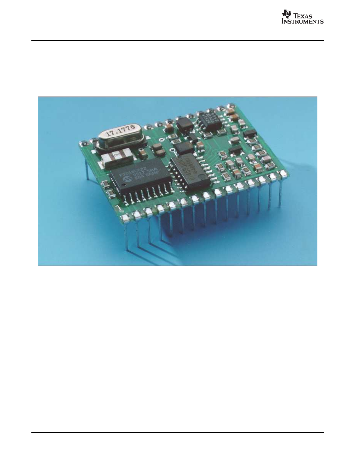
Figure 1-1. Micro-reader Module
1.2 Product Description
The Micro-reader module is a plug-in module which can be plugged into or soldered onto an application
specific adapter board. It supports serial data communications between a PC and TIRIS transponders.
With its Serial Communications Interface (SCI) the Micro-reader supports TTL data communications,
which with the addition of a communications driver (for example: RS232 or RS422) allows communication
to a standard interface.
The Micro-reader can be controlled remotely by either providing certain inputs with the corresponding
voltage level or sending commands to the SCI. It can be driven either with or without synchronization - the
synchronization can be either wireless or wired to enable reliable operation in multi-reader environments.
Two outputs show the reader status and inform the user about a successful command execution. The
Micro-reader supports all available TIRIS™ LF transponders.
10 Product Description SCBU027 – May 2000
Submit Documentation Feedback
Page 11

www.ti.com
1.2.1 Power Supply
1.2.2 Antenna
Product Description
There are two separate 5V supplies to the Micro-reader, one for the output stage (VSP) and the other for
the logic (VSL). On power up VSL should rise faster than 0.1 V/ms to ensure a reliable operation. The
Micro-reader has an on-board reset circuit which will reset it should the supply fall below 4 V ( ± 0.2 V).
In order to avoid problems with noise conducted via the supply lines, we recommend that if a single supply
is used, separate connections from a common de-coupling capacitor are used to feed the Micro-reader.
Note: The RF Module must not be supplied by Switched Mode Power Supplies (SMPS). This is
because most SMPS operate at frequencies around 50 kHz. The harmonics of the
generated field can interfere with the TIRIS receiver. Therefore only use linear regulated
power supplies, or SMPS with a fundamental operating frequency of 200 kHz or higher.
The Micro-reader has been designed for use with a 47 µ H antenna with a Q of 10 to 20 to generate the
exciter frequency of 134.2 kHz. Because of the low Q the system does not need to be tuned.
WARNING
CARE MUST BE TAKEN WHEN HANDLING THE MICRO-READER
AS HIGH VOLTAGES ACROSS THE ANTENNA PINS COULD BE
HARMFUL TO YOUR HEALTH.
1.2.3 Synchronization
There are two possible methods of wired synchronization:
1. Connect a pulse waveform to all RDEN- input pins of the Micro-readers to be synchronized. The pulse
would normally be at VSL, dropping to GND for 100 µ s every 200 ms.
2. Connect all SYNC outputs to an 'Or' and then connect this as an input to RDEN- of each Micro-reader
to be synchronized.
Wireless synchronization of the Micro-reader is very effective at synchronizing to adjacent readers,
however problems may occur if the antennas are positioned such that a transponder can be within range
of two readers at the same time. In this situation one reader could synchronize with the transponder
instead of the other reader.
When the WLSC input is active the Micro-reader is in wireless synchronization mode. Wireless
synchronization can also be switched on/off by a corresponding command via the serial interface. During
execution of this command it has priority over the WLSC input. After the command execution the status of
the WLSC input will be considered again.
Note: It is not recommended to have both wired and wireless synchronization switched on as
synchronization could be unreliable.
We recommend the use of bus drivers for wired synchronization with other Micro-readers
and to prevent ESD damage.
Wired or wireless synchronization prolongs the cycle time by typically 20 ms.
SCBU027 – May 2000 Product Description 11
Submit Documentation Feedback
Page 12

www.ti.com
Product Description
1.2.4 Trigger Mode
When the Micro-reader is in idle mode it is possible to trigger a single charge-only read with a power burst
duration of 50 ms by taking the RDEN- pin to logic high for 100 µ s. The single read will start on the falling
edge of the 100 µ s pulse.
If a transponder command is sent to the Micro-reader via the SCI while RDEN- is in a logic high state
(waiting position), a falling edge would trigger execution of the command. In waiting position the
Micro-reader can only store one command. This means that if two commands were to be sent to the
Micro-reader while it is in the waiting position the second command will overwrite the first one.
1.2.5 Continuous Mode
When the CRDM input is active the Micro-reader goes into continuous charge-only read mode using a
power burst duration of 50 ms. The serial data input takes priority over the CRDM input such that if a
serial command is received it will be executed regardless of the state of the CRDM input. After the
execution of the serial data command the Micro-reader continues with the previous read mode.
In the default continuous read mode, only those valid RO, R/W or MPT IDs that differ from the previously
read ID; or valid IDs read after a “NO READ”, are transferred via the SCI (Normal Mode). The
Micro-reader can be set to transfer all valid IDs that are read (Line Mode) by means of a corresponding
serial data command.
Without synchronization the Micro-reader has a reading frequency of approximately 10 readouts per
second using a power burst duration of 50 ms. Timing is given in more detail in Section 3.2 .
1.2.6 Serial Communication
The two serial I/O pins are configured for 9600 Baud, 1 start bit, 8 data bits, no parity and 1 stop bit; they
can be connected directly to a communications driver to allow a half duplex communication with a PC via
its serial communications interface (for example: RS232 or RS422).
The communications protocol is specified in Chapter 2 .
Handshake
The Micro-reader accepts handshake commands X
stops its current operation and stops transmitting data via the serial port. It stays in idle mode until X
(11
) is received when it continues with the previous mode/command. During this idle period the
hex
Micro-reader accepts commands via the serial port, however, it waits for its execution until X
In this idle period the Micro-reader can store only one command.
Note: While receiving a command protocol from the serial port Xon/X
data without affecting the serial communication.
/X
. When it receives an X
on
off
is interpreted as normal
off
(13
off
) the Micro-reader
hex
on
is received.
on
Product Description12 SCBU027 – May 2000
Submit Documentation Feedback
Page 13
www.ti.com
1.3 Connector Pins
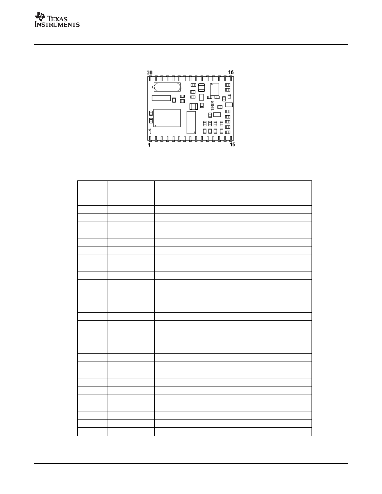
The Micro-reader module has 30 pin connections which are shown in Figure 1-2 and listed in Table 1-1 .
Connector Pins
Figure 1-2. Micro-reader Pin Connections
Table 1-1. Pin Connections
Pin Signal Name Function
1 SYNC Output for wired synchronization
2 RDEN- Input for wired synchronization and single read trigger
3 – Reserved, do not connect
4 RESET- Reset of the Micro-reader
5 RXD Receive Data signal input of serial interface
6 TXD Transmit Data signal output of serial interface
7 – Reserved, do not connect
8 – Reserved, do not connect
9 – Reserved, do not connect
10 – Reserved, do not connect
11 – Reserved, do not connect
12 – Reserved, do not connect
13 – Reserved, do not connect
14 – Reserved, do not connect
15 GND Ground for logic
16 ANT1 Antenna terminal 1
17 ANTCAP Antenna capacitor terminal
18 – Reserved, do not connect
19 ANT2 Antenna terminal 2
20 – Reserved, do not connect
21 GNDP Ground for output stage
22 VSP Supply voltage output stage
23 – Reserved, do not connect
24 VSL Supply voltage logic
25 GND Ground for logic
26 CRD Input for continuous read mode
27 WLS Input to switch wireless synchronization on
28 – Reserved, do not connect
29 OKT Output to show if a valid ID was read
30 STAT Output to show status of RF-transmitter control signal
SCBU027 – May 2000 Product Description 13
Submit Documentation Feedback
Page 14

www.ti.com
Connector Pins
1.3.1 Pin Connection Description
SYNC (1) Output for wired synchronization. This output is at GND level until the Micro-reader starts
RDEN- (2) Input for wired synchronization. Taking this pin to VSL acts as a hold-off for the
RESET- (4) Taking this pin to GND holds the Micro-reader in reset. If the reset pin is not used it can
RXD (5) Input configured to receive serial data commands at 9600 Baud, 1 start bit, 8 data bits,
TXD (6) Output configured to transmit serial data at 9600 Baud, 1 start bit, 8 data bits, no parity
GND (15, 25) Pins 15 and 25 are ground for the logic part.
ANT1 (16) Antenna pin for the connection of 47 µ H, low Q antennas.
ANTCAP (17) It is possible to use antennas of lower inductance by connecting a suitable capacitor
ANT2 (19) Antenna pin (GND) for the connection of 47 µ H, low Q antennas.
GNDP (21) Pin 21 is ground for the output stage.
VSP (22) Pin 22 is for connecting the positive supply voltage (5 V) for the output stage.
VSL (24) Pin 24 is for connecting the positive supply voltage (5 V) for the logic part.
CRDM (26) Supplying pin 26 with a logic high signal causes the Micro-reader to run in a continuous
WLSC (27) Pin 27 enables or disables wireless synchronization. To enable the wireless
its read cycle, at which time it goes to VSL until the complete reading, programming or
locking cycle is finished.
Micro-reader's output stage preventing it from transmitting until the input returns to GND.
The Micro-reader only samples this input at the start of its own reading, programming or
locking cycle, this means that if the input goes to VSL after a cycle is started, the cycle is
not interrupted. RDEN- is a high impedance input and must be tied to GND via a suitable
resistor (27 k Ω ) when it is not being used.
When the Micro-reader is idle it is possible to trigger a single read by taking the
RDEN-pin logic high for 100 ms. The single read will start on the falling edge of the
100 ms pulse.
be left disconnected as it is internally pulled up. Minimum pulse duration to perform a
reset is 1 ms. After a reset the processor takes between 28 ms and 132 ms (typically
72 ms) before it can receive new instructions via the serial communications interface.
no parity and 1 stop bit.
and 1 stop bit.
between ANT1 and ANTCAP. This additional capacitor (ceramic, 100 VDC) will be in
parallel with the 30 nF resonance capacitor on board the Micro-reader (see Figure 1-4
and Appendix C ).
charge-only read mode (see Section 1.2.5 for more information).
When the CRDM pin is tied to logic low, the Micro-reader is in an idle state waiting for
commands via the serial interface or for a trigger signal (RDEN-) to start a single read
out cycle. CRDM is a high impedance input and must be tied to either VSL or GND via a
suitable resistor (27 k Ω ).
synchronization, pin 27 must be taken to VSL. When wireless synchronization is
enabled, the Micro-reader will try to synchronize its transmit signals with any other
readers in range. To disable wireless synchronization pin 27 must be taken to GND. Pin
27 is a high impedance input and must be tied to either VSL or GND via a suitable
resistor (27 k Ω ).
Wireless synchronization can also be switched on/off by a corresponding command via
the serial interface. During execution of this command it has priority over the WLSC
input.
14 Product Description SCBU027 – May 2000
Submit Documentation Feedback
Page 15

www.ti.com
RESET-
CRDM
RDEN-
SYNC
OKT
STAT
TXD
RXD
GND
VSL
GNDP
MICRO
CONTROLLER
RFM
ASIC
ANT1
ANT2
ANTCAP
Power
stage
Filter
RXCK
RXDT-
TXCT-
VSL
VSP
VSL
WLSC
VSP
OKT (29) This output is set to logic high for approx. 60 ms if a valid transponder was read. It can
be connected to an LED externally to indicate the result of the read cycle.
STAT(30) Pin 30 is set to logic low when the RF-transmitter is activated. Supplying an external LED
with this signal makes the status of the Micro-reader visible.
1.3.2 Module and Antenna Block Diagrams
Connector Pins
Figure 1-3. Block Diagram of the Micro-reader
SCBU027 – May 2000 Product Description 15
Submit Documentation Feedback
Page 16

www.ti.com
ANT1
ANT2
ANTCAP
TXHI
from
ASIC
TXLO
from
ASIC
VSP
RECEIVE
RESONANCE
CAPACITOR
Connector Pins
Figure 1-4. Antenna Circuit Block Diagram
16 Product Description SCBU027 – May 2000
Submit Documentation Feedback
Page 17

SCBU027 – May 2000
Communications Protocol
This chapter describes the protocol that you need to use to send instructions from your
PC to the Micro-reader. It also describes the protocol that the Micro-reader uses to
respond to the PC.
Topic .................................................................................................. Page
2.1 Protocol PC to Micro-reader ....................................................... 18
2.2 Protocol Micro-reader to PC ....................................................... 20
Chapter 2
SCBU027 – May 2000 Communications Protocol 17
Submit Documentation Feedback
Page 18

www.ti.com
Byte Contents (hexadecimal value)
0 Start Mark (SOH, 01
hex
)
1 Length
2 Command Field (1)
3 Command Field (2) (optional)
4(3) Data Field (1)
.
.
N+3(2) Data Field (N)
N+4(3) BCC
Start Length
BCC
Cmd 1 Cmd 2 Data
Protocol PC to Micro-reader
2.1 Protocol PC to Micro-reader
Examples are given in Section 5.1 .
Note: The total number of bytes sent within a protocol frame (including Start Mark and BCC) is
limited to 41 bytes.
2.1.1 Start Mark
The 'Start-Mark' signifies the beginning of a message. It is represented by the ASCII character SOH (Start
Of Header, 01
).
hex
2.1.2 Length
The 'Length' byte indicates the length, in bytes, of the following Command and Data Fields.
2.1.3 Command Field
The 'Command Field(s)' defines the mode in which the Micro-reader operates and determines the
operation that is to be carried out in the transponder. Depending on the setting of the relevant bits, the
corresponding information specified in the Data Fields will be sent to the transponder or not. Thus all
functions of each particular transponder type can be executed (see 2.1.4 for further information).
Command Field (1)
Bit Use Setting Comment
0/1 Mode/Cmd
2 FBCC Calculation 1/0 If set, Micro-reader calculates FBCC of the MPT protocol
3 Power Burst I 1/0 If set, needs to be determined in Data Field (see Section 2.1.4 )
4 Power Pause Duration 1/0 If set, needs to be determined in Data Field
5 Power Burst II 1/0 If set, needs to be determined in Data Field
6 Data 1/0 If set, needs to be determined in Data Field
7 Cmd Expansion Field 1/0 If set, Command Field (2) follows
Communications Protocol18 SCBU027 – May 2000
00
(MSB,LSB)
01 Read in continuous Normal Mode
10 Read in continuous Line Mode
11 Send Micro-reader S/W version
Perform single command (for example: single read, program, lock)
Submit Documentation Feedback
Page 19

www.ti.com
Example: E8
Hex
= 1110 1000
BIN
1 1 1 0 1 0 0 0
Perform single command
No FBCC calculation
Power burst I value set in Data Field
Default set to 0
Power burst II value set in Data Field
Data values follows in Data Field
Command Field (2) follows
Example: 06
Hex
= 0000 0110
BIN
0 0 0 0 0 1 1 0
No Special Write Timing
Wireless Synchronization is used
Micro-reader calculates DBCC
Bits 3-7 reserved
Protocol PC to Micro-reader
If bit 5 (Power Burst II, for example: for programming and locking) is set, the Microreader automatically
operates in single mode. Thus the user is enabled to validate the programming or lock response before a
further cycle is started.
If bit 2 (FBCC calculation) and bit 6 (Data) are set, the Micro-reader automatically calculates a two byte
BCC over the data to be sent to the transponder and adds it to the protocol. When bits 2 and 6 are set the
PC must not send the 2 byte FBCC to the Micro-reader.
Bit 4 (Power Pause Duration) is for future use and must not be set when addressing standard TIRIS
transponders.
Command Field (2)
Bit Use Setting Comment
0 Special Write Timing 1/0 If set, needs to be determined in Data Field (see Section 2.1.4 )
1 Wireless Synchronization 1/0 If set, wireless synchronization is used
2 DBCC calculation 1/0 If set, Micro-reader calculates DBCC of the R/W and MPT write data
3–7 Reserved
SCBU027 – May 2000 Communications Protocol 19
Submit Documentation Feedback
If Command Field (2) is not present, standard TIRIS write timings are used and wireless synchronization is
switched on/off according to the status of input line WLSC.
Note: The settings specified in Command Field (1) and (2) are only valid during the execution of
the current command.
Page 20

www.ti.com
Example: 02 08 32
02 0000 0010
08 0000 1000
--------------------------------
XOR 0000 1010
32 0011 0010
--------------------------------
XOR 0011 1000 = 38 (hex)
Byte Contents (hexadecimal value)
0 Start Mark (SOH, 01
hex
)
1 Length
2 Status
3 Data Field (1) (LSByte)
.
.
.
N+2 Data Field (N) (MSByte)
N+3 BCC
Start
Length
BCC
Status Data
Protocol Micro-reader to PC
2.1.4 Data Field
The presence of the relevant data field depends on the setting of the bits in the Command Field.
If the relevant bit (for example: Command bit 3 “Power Burst I”) is set to “1”, then Data Field 1 is present
defining the Power Burst length. If the relevant bit in the Command Field is set to “0” the consequent Data
Field is omitted, this results in the following data field being moved forward (decremented) by one.
Data Field Use Range (dec) Comment
1 Power Burst I 1..255 ms If bit 3 of Command Field(1) is set
2 Power Pause Duration 1..255 ms If bit 4 of Command Field(1) is set
3 Power Burst II 1..255 ms If bit 5 of Command Field(1) is set
4/5 toffLow (LSByte/MSByte) 28..2044 ms If bit 0 of Command Field(2) is set
6/7 tonLow (LSByte/MSByte) 28..2044 ms If bit 0 of Command Field(2) is set
8/9 toffHigh (LSByte/MSByte) 28..2044 ms If bit 0 of Command Field(2) is set
10/11 tonHigh (LSByte/MSByte) 28..2044 ms If bit 0 of Command Field(2) is set
12 # of Data Fields that follow See
13.. Data Fields LSByte first
(1)
The number of Data Fields must not cause an infringement of the total number of bytes allowed within a protocol frame.
Transponder command protocols are described in detail in Section 4.1 .
2.1.5 BCC
The 'BCC' field is a one-byte value of the Longitudinal Redundancy Check calculation (Xor'ed bytes) for
the preceding message. The calculation is performed on the whole message excluding the Start-Mark.
(1)
If bit 6 of Command Field(1) is set
2.2 Protocol Micro-reader to PC
See Section 5.2 for examples.
20 Communications Protocol SCBU027 – May 2000
Submit Documentation Feedback
Page 21

www.ti.com
2.2.1 Start Mark
2.2.2 Length
2.2.3 Status
Protocol Micro-reader to PC
The 'Start-Mark' signifies the beginning of a message. It is represented by the ASCII character SOH (Start
Of Header: 01
)
hex
The 'Length' byte indicates the length, in bytes, of the following Status and Data Fields.
The 'Status' byte provides feedback from the preceding read or program operation.
Status Bits Setting Comment
00
(MSB,LSB)
0,1
2 1/0 If set, Startbyte detected
3 1/0 If set, DBCC O.K.
4 1/0 If set, FBCC O.K.
5 1/0 If set, Micro-reader S/W version follows
6–7 Reserved
01 Transponder type: R/W
10 Transponder type: MPT/SAMPT
11 Other
Transponder type: RO
2.2.4 Data Field
2.2.5 BCC
Response Type Comment
RO 8 Identification Data (LSByte first), see Section 4.2.1
R/W 8 Identification Data (LSByte first)), see Section 4.2.2
MPT/SAMP 9
Other 14
No read 0
S/W version 1 For example: 15
# of Bytes in Data
Field
Identification Data (LSByte first), plus Read Address, see
Section 4.2.3
Complete transponder protocol without pre-bits provided that
a valid RO or R/W start byte was detected
No Data Fields, not even transponder start byte was
detected, status 03
hex
means S/W version 1.5
hex
Section 4.2 provides an overview of the response telegrams of the current TIRIS transponder types.
The 'BCC' field is a one-byte value of the Longitudinal Redundancy Check calculation (Xor'ed bytes) for
the preceding message. The calculation is performed on the whole message excluding the Start-Mark. An
example is shown in Section 2.1.5 .
SCBU027 – May 2000 Communications Protocol 21
Submit Documentation Feedback
Page 22

www.ti.com
Communications Protocol22 SCBU027 – May 2000
Submit Documentation Feedback
Page 23

Specifications
This chapter provides the specifications for the Micro-reader, its inputs and outputs,
and its timing.
Topic .................................................................................................. Page
3.1 Recommended Operating Conditions .......................................... 24
3.2 Timings .................................................................................... 24
3.3 Mechanical Data........................................................................ 25
Chapter 3
SCBU027 – May 2000
SCBU027 – May 2000 Specifications 23
Submit Documentation Feedback
Page 24

www.ti.com
Recommended Operating Conditions
3.1 Recommended Operating Conditions
Operating free-air temperature range T_oper –25 to +70 ° C
Storage temperature range T_store –40 to +85 ° C
Note: Free-air temperature: air temperature immediately surrounding the Module. If the module
is incorporated into a housing, it must be guaranteed by proper design or cooling that the
internal temperature does not exceed the absolute maximum ratings.
Symbol Parameter Min Typ Max Unit
V_VSP Supply voltage for power stage 4.5 5.0 5.5 V
V_VSL Supply voltage for logic 4.5 5.0 5.5 V
I_VSP Supply current for power stage 10
I_VSL Supply current for logic 30
I_su Output current sunk by an output pin 5.0 15.0 mA
I_so Output current sourced by an output pin 5.0 15.0 mA
I_sutot Output current sunk by all output pins 20.0 60.0 mA
I_sotot Output current sourced by all output pins 20.0 60.0 mA
V_ret VSP start voltage to ensure power on reset GND V
Vrise_ret VSP rise rate to ensure power on reset 0.1 V/ms
I_idle Supply current with Micro-reader idle 5.0 mA
I_act Supply current with Micro-reader active 100
ViH Input high voltage 0.8VSL VSL V
ViL Input low voltage GND 0.2VSL V
VoH Output high voltage VSL – 0.7 VSL V
VoL Output low voltage GND 0.6 V
Q_Ant Antenna quality factor 10 15 20
L_Ant Antenna inductance value 46.1 47.0 47.9 µ H
(1)
Typical supply current (peak value) for the power stage when the RF transmitter is switched on (L = 47 µ H, Q = 12).
(2)
Typical supply current for logic when the RF transmitter is switched on.
(3)
Typical supply current (average value) of the Micro-reader when the RF transmitter is switched on (L = 47 µ H, Q = 12).
(1)
(2)
(3)
mA
mA
mA
3.2 Timings
Parameter Typ Max Unit
Read Cycle time without synch (no read) 100 105 ms
Read Cycle time with synch (no read) 120 175 ms
Read Cycle time without synch (valid read) 170 175 ms
Read Cycle time with synch (valid read) 190 245 ms
Interbyte time-out for serial communication 10
(1)
If an Interbyte time-out occurs the Micro-reader performs a reset.
Specifications 24 SCBU027 – May 2000
(1)
ms
Submit Documentation Feedback
Page 25

www.ti.com
3.3 Mechanical Data
Recommended finished pin hole size is 1 mm diameter.
Mechanical Data
Parameter Min Typ Max Unit
Length 37.9 38.3 38.7 mm
Width 28.8 29.3 29.6 mm
Height including pins 12.5 13.5 14.0 mm
Weight 5.0 g
Figure 3-1. Top, Front, and Side Views (Measurements in mm)
SCBU027 – May 2000 Specifications 25
Submit Documentation Feedback
Page 26

www.ti.com
Specifications 26 SCBU027 – May 2000
Submit Documentation Feedback
Page 27

Transponder Protocols
This chapter describes the protocols used when sending commands to the transponder
and the protocols used by the transponder when responding.
Topic .................................................................................................. Page
4.1 Transponder Commands............................................................ 28
4.2 Transponder Responses ............................................................ 30
Chapter 4
SCBU027 – May 2000
SCBU027 – May 2000 Transponder Protocols 27
Submit Documentation Feedback
Page 28

www.ti.com
OFF
ON
READ
50 ms 20 ms
RF TRANSMITTER
POWER BURST
READ
20 ms
50 ms
WRITE
KEYWORD
8
80 16
16 ms 160 ms 32 ms
15 ms
PASSWORD
8
16 ms
112 bit
309 ms
WRITE WRITE
FRAME
WRITE DATA
128 bit
LSB MSB
OFF
ON
POWER BURST I
PB II
RF TRANSMITTER
Write Keyword
:
BB
hex
Write Password
:
EB
hex
Write Frame
:
0300
hex
WRITE ADDRESS
MSB LSB
P P P P P P
C C
| |
PAGE COMMAND
MSB LSB MSB LSB
Page 1 000001 00 General read page
Page 2 000010 01 Program page
. . . 10 Lock page
Page 16 010000 11 Selective read
Page 17 010001
Transponder Commands
4.1 Transponder Commands
This section describes the protocols that need to be sent by the PC to the transponder via the
Micro-reader in order to execute the required function.
4.1.1 Read RO, R/W
4.1.2 Program R/W
Figure 4-1. Read Function
Figure 4-2. Programming Data Format of the 64-bit Read/Write Transponder
4.1.3 Addressing MPTs/SAMPTs
Since MPT/SAMPTs allow the execution of the different commands applicable to multiple pages the 'Write
Address' needs to be sent within the protocol in order to determine the function to be executed with a
specific MPT/SAMPT page.
28 Transponder Protocols SCBU027 – May 2000
Submit Documentation Feedback
Page 29

www.ti.com
4.1.3.1 General Read Page of MPT/SAMPT
50 ms
READ
WRITE
ADDRESS
86 ms
LSB
8 bit
20 ms16 ms
ON
OFF
POWER BURST I
RF TRANSMITTER
128 bit
READ OR
20 ms50 ms
WRITE
ADDRESS
WRITE DATA WRITE FRAME BCC
8 8 0 1 6
16 ms 160 ms 32 ms 15 ms
293 ms
104 bit 128 bit
LSB
DISCHARGE
MSB
RF
OFF
ON
TRANSMITTER
POW ER BURST I
PB II
50 ms
WRITE
ADDRESS
8
WRITE FRAME BCC
16
32 ms
133 ms
24 bit
READ OR
20 ms
128 bit
DISCHARGE
15 ms
LSB
16 ms
MSB
ON
OFF
POWER BURST I
RF TRANSMITTER
PB II
50 ms
WRITE
ADDRESS
8
WRITE FRAME BCC
16
32 ms
READ OR
20 ms
128 bit
DISCHARGE
LSB MSB
16 ms
SELECTIVE
ADDRESS
ON
OFF
RF TRANSMITTER
POWER BURST I
8 - 32
16 - 64 ms
134 - 182 ms
32 - 56 bit
4.1.3.2 Program Page of MPT/SAMPT
Transponder Commands
Figure 4-3. Data Format of the General Read Page Function
4.1.3.3 Lock Page of MPT/SAMPT
4.1.3.4 Selective Read Page of SAMPT
Figure 4-4. Programming Data Format of the MPT
Figure 4-5. Lock Page of MPT/SAMPT
Figure 4-6. Data Format of the Selective Read Page Function
SCBU027 – May 2000 Transponder Protocols 29
Submit Documentation Feedback
Page 30

www.ti.com
50 ms
WRITE
ADDRESS
8
16 ms
READ OR
20 ms
80
16
160 ms 32 ms 15 ms
128 bit
LSB
DISCHARGE
WRITE FRAME BCCWRITE DATA
MSB
ADDRESS
SELECTIVE
ON
OFF
RF T RANSMITTER
POW ER BURST I
PB II
309 - 357 ms
112 - 136 bit
8 - 32
16 - 64 ms
50 ms
WRITE
ADDRESS
8
16 ms
READ OR
20 ms
16
32 ms 15 ms
128 bit
LSB
DISCHARGE
WRITE FRAME BCC
MSB
ADDRESS
SELECTIVE
ON
OFF
RF T RANSMITTER
POW ER BURST I
PB II
8 - 32
16 - 64 ms
32 - 56 bit
149 - 197 ms
START
816 8
STOP
64 16
DISCHARGE
LSB
PRE BITS
END BITS
IDENTIFICATION DATA DATA BCC
MSB
16 bits
16
112 bits
READ DATA
START
816 8
READ DATA
STOP
64 16
DISCHARGE
15
LSB
PRE BITS END BITS
IDENTIFICATION DATA DATA BCC
MSB
112 bits 16 bits
IDENT. DATA
Transponder Responses
4.1.3.5 Selective Program Page of SAMPT
Figure 4-7. Data Format of the Selective Program Page Function
4.1.3.6 Selective Lock Page of SAMPT
4.2 Transponder Responses
This section shows the response telegrams of the current TIRIS transponder types.
4.2.1 Read Only Transponder
4.2.2 Read/Write Transponder
Figure 4-8. Data Format of the Selective Lock Page Function
Figure 4-9. RO Read Data Format
Figure 4-10. R/W Read Data Format
Transponder Protocols30 SCBU027 – May 2000
Submit Documentation Feedback
Page 31

www.ti.com
START
8
16
8
16
READ DATA
ADDR.
READ
128 bit
64
16
LSB
IDENTIFICATION DATA
MSB
FBCC
DBCC
PRE BITS
DISCHARGE
READ ADDRESS
MSB LSB
P P P P P P C C
| |
PAGE COMMAND
MSB LSB MSB LSB
Page 1 000001 00 Read unlocked page
Page 2 000010 01 Programming done
. . . 10 Read locked page
Page 16 010000 11 Reserved (see Note A)
Page 17 010001
000000 00 Read unlocked page, locking not correctly executed
000000 01 Programming done, but possibly not reliable
000000 10 Read locked page, but locking possibly not reliable
Transponder Responses
4.2.3 MPT/SAMPT
Figure 4-11. MPT/SAMPT Read Data Format
The Read Address consists of a 2-bit status field and a 6-bit page field. The status field provides
information about the function the multipage transponder has executed and the page field shows which
page was affected.
A If the status indicates 'Reserved', the read data cannot be interpreted as identification data.
Note: It is strongly recommended to verify whether the requested function has actually been
carried out in the transponder by checking the Read Address. If a 'not reliable' response
message is received, the command must be sent again to guarantee transponder data
retention.
SCBU027 – May 2000 Transponder Protocols 31
Submit Documentation Feedback
Page 32

www.ti.com
Transponder Protocols32 SCBU027 – May 2000
Submit Documentation Feedback
Page 33

Communication Protocol Examples
This chapter provides some examples of some actual commands sent to a transponder
and some possible responses.
Topic .................................................................................................. Page
5.1 PC to Micro-reader .................................................................... 34
5.2 Micro-reader to PC .................................................................... 38
Chapter 5
SCBU027 – May 2000
SCBU027 – May 2000 Communication Protocol Examples 33
Submit Documentation Feedback
Page 34

www.ti.com
PC to Micro-reader
5.1 PC to Micro-reader
5.1.1 Read RO, R/W
5.1.2 Program R/W Transponder
The following sequence of bytes programs a R/W transponder with:
Byte Comment Description
0 01 Start Mark
1 02 Length Two bytes follow excluding BCC
2 08 Command Field (1) Perform Single command, send Power Burst I
3 32 Data Field (1) Power Burst I with 50 ms duration (charge-up)
4 38 BCC BCC over previous bytes excluding Start Mark
Content
(hex)
00 00 00 00 00 00 00 01
MSByte LSByte
Byte Comment Description
0 01 Start Mark
1 11 Length 17 bytes follow excluding BCC
2 E8 Command Field (1)
3 06 Command Field (2) Wireless synchronization, calculate DBCC of the R/W and MPT write data
4 32 Data Field (1) Power Burst I with 50 ms duration (charge-up)
5 0F Data Field (2) Power Burst II with 15 ms duration (Progr. burst)
6 0C Data Field (3) 12 Data Fields follow
7 BB Data Field (4) Write Keyword
8 EB Data Field (5) Write Password
9 01 Data Field (6) Programming data (LSByte)
10 00 Data Field (7) Programming data
11 00 Data Field (8) Programming data
12 00 Data Field (9) Programming data
13 00 Data Field (10) Programming data
14 00 Data Field (11) Programming data
15 00 Data Field (12) Programming data
16 00 Data Field (13) Programming data (MSByte)
17 00 Data Field (14) Write Frame
18 03 Data Field (15) Write Frame
19 9C BCC BCC over previous bytes excluding Start Mark
Content
(hex)
Perform Single command, no FBCC calculation, send Power Burst I and II
with Data Command Field (2) follows
Communication Protocol Examples34 SCBU027 – May 2000
Submit Documentation Feedback
Page 35

www.ti.com
5.1.3 General Read Page of MPT
The following sequence of bytes reads page 2 of an MPT.
Byte Comment Description
0 01 Start Mark
1 04 Length Four bytes follow excluding BCC
2 48 Command Field (1) Perform Single command, send Power Burst I with data
3 32 Data Field (1) Power Burst I with 50 ms duration (charge-up)
4 01 Data Field (2) One Data Field follows
5 08 Data Field (3) Write Address specifying General Read Page 2
6 77 BCC BCC over previous bytes excluding Start Mark
Content
(hex)
5.1.4 Program Page of MPT
The following sequence of bytes programs page 2 of an MPT with:
00 00 00 00 00 2D C6 47
MSByte LSByte
PC to Micro-reader
Byte Comment Description
0 01 Start Mark
1 0F Length 15 bytes follow excluding BCC
2 6C Command Field (1) Perform Single command, calculate FBCC, send Power Burst I & II with Data
3 32 Data Field (1) Power Burst I with 50 ms duration (charge-up)
4 0F Data Field (2) Power Burst II with 15 ms duration (Progr. burst)
5 0B Data Field (3) 11 Data Fields follow
6 09 Data Field (4) Write Address specifying Program Page 2
7 47 Data Field (5) Programming data (LSByte)
8 C6 Data Field (6) Programming data
9 2D Data Field (7) Programming data
10 00 Data Field (8) Programming data
11 00 Data Field (9) Programming data
12 00 Data Field (10) Programming data
13 00 Data Field (11) Programming data
14 00 Data Field (12) Programming data (MSByte)
15 96 Data Field (13) DBCC (LSByte)
16 50 Data Field (14) DBCC (MSByte)
17 36 BCC BCC over previous bytes excluding Start Mark
Content
(hex)
SCBU027 – May 2000 Communication Protocol Examples 35
Submit Documentation Feedback
Page 36

www.ti.com
PC to Micro-reader
5.1.5 Lock Page of MPT
The following sequence of bytes locks page 2 of an MPT.
Byte Comment Description
0 01 Start Mark
1 05 Length Five bytes follow excluding BCC
2 6C Command Field (1) Perform Single command, calculate FBCC, send Power Burst I & II with data
3 32 Data Field (1) Power Burst I with 50 ms duration (charge-up)
4 07 Data Field (2) Power Burst II with 15 ms duration (Progr. burst)
5 01 Data Field (3) One Data Field follows
6 0A Data Field (4) Write Address specifying Lock Page 2
7 5F BCC BCC over previous bytes excluding Start Mark
Content
(hex)
5.1.6 Selective Read Page of SAMPT
The following sequence of bytes reads page 2 of an SAMPT.
The 24 bit selective address =
12 34 56
MSByte LSByte
Byte Comment Description
0 01 Start Mark
1 07 Length 7 bytes follow excluding BCC
2 4C Command Field (1) Perform Single command, calculate FBCC, send Power Burst I with Data
3 32 Data Field (1) Power Burst I with 50 ms duration (charge-up)
4 04 Data Field (2) 4 Data Fields follow
5 0B Data Field (3) Write Address specifying selective Read Page 2
6 56 Data Field (4) Selective Address LSB
7 34 Data Field (5) Selective Address
8 12 Data Field (6) Selective Address MSB
9 06 BCC BCC over previous bytes excluding Start Mark
Content
(hex)
Communication Protocol Examples36 SCBU027 – May 2000
Submit Documentation Feedback
Page 37

www.ti.com
5.1.7 Selective Program Page of SAMPT
The following sequence of bytes selective programs page 2 of an SAMPT with:
00 00 00 00 00 00 00 11
MSByte LSByte
The 24 bit selective address =
12 34 56
MSByte LSByte
PC to Micro-reader
Byte Comment Description
0 01 Start Mark
1 12 Length 18 bytes follow excluding BCC
2 6C Command Field (1) Perform Single command, calculate FBCC, send Power Burst I & II with Data
3 32 Data Field (1) Power Burst I with 50 ms duration (charge-up)
4 0F Data Field (2) Power Burst II with 15 ms duration (Progr. burst)
5 0E Data Field (3) 14 Data Fields follow
6 09 Data Field (4) Write Address specifying Program Page 2
7 56 Data Field (5) Selective Address LSB
8 34 Data Field (6) Selective Address
9 12 Data Field (7) Selective Address MSB
10 11 Data Field (8) Programming data (LSByte)
11 00 Data Field (9) Programming data
12 00 Data Field (10) Programming data
13 00 Data Field (11) Programming data
14 00 Data Field (12) Programming data
15 00 Data Field (13) Programming data
16 00 Data Field (14) Programming data
17 00 Data Field (15) Programming data (MSByte)
18 9F Data Field (16) DBCC (LSByte)
19 BD Data Field (17) DBCC (MSByte)
20 34 BCC BCC over previous bytes excluding Start Mark
Content
(hex)
SCBU027 – May 2000 Communication Protocol Examples 37
Submit Documentation Feedback
Page 38

www.ti.com
Micro-reader to PC
5.1.8 Selective Lock Page of SAMPT
The following sequence of bytes locks page 2 of an SAMPT.
The 24 bit selective address =
12 34 56
MSByte LSByte
Byte Comment Description
0 01 Start Mark
1 08 Length 8 bytes follow excluding BCC
2 6C Command Field (1) Perform Single command, calculate FBCC, send Power Burst I & II with Data
3 32 Data Field (1) Power Burst I with 50 ms duration (charge-up)
4 0F Data Field (2) Power Burst II with 15 ms duration (Progr. burst)
5 04 Data Field (3) 4 Data Fields follow
6 0A Data Field (4) Write Address specifying selective Lock Page 2
7 56 Data Field (5) Selective Address LSB
8 34 Data Field (6) Selective Address
9 12 Data Field (7) Selective Address MSB
10 27 BCC BCC over previous bytes excluding Start Mark
Content
(hex)
5.2 Micro-reader to PC
5.2.1 Successful Read of RO
Byte Comment Description
0 01 Start Mark
1 09 Length 9 bytes follow excluding BCC
2 0C Status Valid RO, Startbyte detected, DBCC O.K.
3 6A Data Field (1) Identification Data (LSByte)
4 58 Data Field (2) Identification Data
5 4C Data Field (3) Identification Data
6 00 Data Field (4) Identification Data
7 00 Data Field (5) Identification Data
8 00 Data Field (6) Identification Data
9 00 Data Field (7) Identification Data
10 00 Data Field (8) Identification Data (MSByte)
11 7B BCC BCC over previous bytes excluding Start Mark
Content
(hex)
Communication Protocol Examples38 SCBU027 – May 2000
Submit Documentation Feedback
Page 39

www.ti.com
5.2.2 Successful Program Page 2 of MPT
Micro-reader to PC
5.2.3 No Read
Byte Comment Description
0 01 Start Mark
1 0A Length 10 bytes follow excluding BCC
2 1E Status Valid MPT, Startbyte detected, DBCC O.K., FBCC O.K.
3 47 Data Field (1) New Identification Data (LSByte)
4 C6 Data Field (2) New Identification Data
5 2D Data Field (3) New Identification Data
6 00 Data Field (4) New Identification Data
7 00 Data Field (5) New Identification Data
8 00 Data Field (6) New Identification Data
9 00 Data Field (7) New Identification Data
10 00 Data Field (8) New Identification Data (MSByte)
11 09 Data Field (9) Read Address specifying successful progr. of page 2
12 B1 BCC BCC over previous bytes excluding Start Mark
Byte Comment Description
0 01 Start Mark
1 01 Length One byte follows excluding BCC
2 03 Status Other, no Startbyte, DBCC not O.K., FBCC not O.K.
3 02 BCC BCC over previous bytes excluding Start Mark
Content
(hex)
Content
(hex)
SCBU027 – May 2000 Communication Protocol Examples 39
Submit Documentation Feedback
Page 40

www.ti.com
Communication Protocol Examples40 SCBU027 – May 2000
Submit Documentation Feedback
Page 41

Appendix A
SCBU027 – May 2000
CE Declaration
The Micro-reader module complies with the European CE requirements specified in the EMC Directive
89/336/EEC. The relevant documentation numbers are:
Declaration of Conformity 11-06-02-005
Type Examination Certificate 11-06-05-001
If the Micro-reader is operated from a mains power supply, all power connections and additional
components of the final device must comply with the European EMC directive.
Additional connections may have a length of up to 2 m maximum, or in fixed installations up to 1 m
maximum.
European customers must themselves make sure that the final device conforms to the European EMC
Directive.
SCBU027 – May 2000 CE Declaration 41
Submit Documentation Feedback
Page 42

www.ti.com
CE Declaration42 SCBU027 – May 2000
Submit Documentation Feedback
Page 43

L78M05CV
ANTENNA
MICROREADER
+
+
+
6
15
14
13
+
12
11
16
2
1
3
4
5
+
RS 232C
+5V
0.1 µF
10 µF
25V
10 µF
25V
10 µF
25V
10 µF
25V
10 µF
25V
10 µF
25V
DC IN
10K
10K
10K
+5V
+ DC IN
0V
SYNC
STAT
OKT
3 2 1
0V
240
Ω
240
Ω
240
Ω
2
26
27
21 15 25
1
30
29
6
5
16192224
RDEN
CRDM
WLSC
+
NB: For design-in we recommend the SIPEX SP232 for the
line driver chip to avoid potential interference problems.
Demonstration Circuit
The Micro-reader module can be demonstrated using the circuit shown in Figure B-1 .
Appendix B
SCBU027 – May 2000
SCBU027 – May 2000 Demonstration Circuit 43
Submit Documentation Feedback
Figure B-1. Micro-reader Demonstration Circuit
Page 44

www.ti.com
Demonstration Circuit44 SCBU027 – May 2000
Submit Documentation Feedback
Page 45

C.1 Introduction
C.2 Antenna Construction
Appendix C
SCBU027 – May 2000
Antenna Design
This appendix gives an example of how you could construct an antenna to work with the Micro-reader. It
also provides information about calculating the Q factor and adapting the inductance range.
The antenna properties should be:
Q factor less than 20
Inductance between 46 µ H and 48 µ H
Recommended maximum size 200 mm × 200 mm
Item List:
Item Description Quantity
1 Enamelled solid copper wire, 0.2 mm 2.1 g
2 Tape, 10 mm wide 20 mm
3 Block cloth tape, 12 mm wide 0.12 m
4 Spiroband, 3 mm diameter 0.24 m
5 Screened antenna lead 1 m
Method:
• Wind 15 turns of item 1 with a diameter of 75 mm.
• Leave about 50 mm free at the ends, cross the wires (at the ± 50 mm point) and secure them together
using the tape (item 2).
• Twist the spriband (item 4) onto the coil that you have just made, leaving the start and finish ends free.
• Strip the insulating braid back at the end of the antenna lead (item 5). Wrap the start and finish ends at
least three times around the bared ends and solder the joints (the polarity is not important).
• Tightly bind the soldered joints to the spriband using the cloth tape (item 3).
This method should result in a 47 µ H antenna with a quality factor of approximately 17 to 18.
SCBU027 – May 2000 Antenna Design 45
Submit Documentation Feedback
Page 46

www.ti.com
Where: f = 134200 Hz (Frequency = 134.2 kHz)
L = Inductance (H)
R = Series resistance ( )Ω
Example:
Inductance (L) = 47 µH
Resistance (R) = 2.2 Ω
= 18
Q =
2 fLπ
R
Q =
2 × × 134200 × 0.000047π
2.2
39.636
2.2
=
–=
1
C
ext
1
C
tot
1
30 nF
Q Factor
C.3 Q Factor
If the antenna’s Q factor exceeds 20:
1. The output capacitors will be overloaded and long term damage could result.
2. The antenna may still be resonating when the response from the transponder is received. Without
built-in damping the data will not be correctly received.
3. The antenna may be detuned if there is any metal in the area.
The following formula provides an approximate method of calculating the Q factor of the antenna:
C.4 Adapting the Inductance Range
If your antenna is outside of the required inductance range of 46 to 48 µ H, you can adapt it to work with
the Micro-reader by adding an external capacitor to it, either in series or in parallel. You can use this
external capacitor to change the inductance range by ± 5 µ H.
You can work out the total resonance capacity using the following formula:
C
= 1 / (4 π2L
tot
If the antenna inductance is less than 46.1 µ H you can add an extra capacitor (externally) to the antenna
between pin 16 (ANT1) and pin 17 (ANTCAP). The formula to work out the value of this capacitor is:
C
= C
ext
tot
If the antenna inductance is more than 47.9 µ H you can add an extra capacitor in series with the antenna
between pin 19 (ANT2) and the antenna. The formula to work out the value of this capacitor is:
– 30 nF
f2)
Ant
46 Antenna Design SCBU027 – May 2000
Submit Documentation Feedback
Page 47

IMPORTANT NOTICE
Texas Instruments Incorporated and its subsidiaries (TI) reserve the right to make corrections, modifications,
enhancements, improvements, and other changes to its products and services at any time and to discontinue
any product or service without notice. Customers should obtain the latest relevant information before placing
orders and should verify that such information is current and complete. All products are sold subject to TI’s terms
and conditions of sale supplied at the time of order acknowledgment.
TI warrants performance of its hardware products to the specifications applicable at the time of sale in
accordance with TI’s standard warranty. Testing and other quality control techniques are used to the extent TI
deems necessary to support this warranty . Except where mandated by government requirements, testing of all
parameters of each product is not necessarily performed.
TI assumes no liability for applications assistance or customer product design. Customers are responsible for
their products and applications using TI components. To minimize the risks associated with customer products
and applications, customers should provide adequate design and operating safeguards.
TI does not warrant or represent that any license, either express or implied, is granted under any TI patent right,
copyright, mask work right, or other TI intellectual property right relating to any combination, machine, or process
in which TI products or services are used. Information published by TI regarding third-party products or services
does not constitute a license from TI to use such products or services or a warranty or endorsement thereof.
Use of such information may require a license from a third party under the patents or other intellectual property
of the third party, or a license from TI under the patents or other intellectual property of TI.
Reproduction of information in TI data books or data sheets is permissible only if reproduction is without
alteration and is accompanied by all associated warranties, conditions, limitations, and notices. Reproduction
of this information with alteration is an unfair and deceptive business practice. TI is not responsible or liable for
such altered documentation.
Resale of TI products or services with statements different from or beyond the parameters stated by TI for that
product or service voids all express and any implied warranties for the associated TI product or service and
is an unfair and deceptive business practice. TI is not responsible or liable for any such statements.
Following are URLs where you can obtain information on other Texas Instruments products and application
solutions:
Products Applications
Amplifiers amplifier.ti.com Audio www.ti.com/audio
Data Converters dataconverter.ti.com Automotive www.ti.com/automotive
DSP dsp.ti.com Broadband www.ti.com/broadband
Interface interface.ti.com Digital Control www.ti.com/digitalcontrol
Logic logic.ti.com Military www.ti.com/military
Power Mgmt power.ti.com Optical Networking www.ti.com/opticalnetwork
Microcontrollers microcontroller.ti.com Security www.ti.com/security
Low Power Wireless www.ti.com/lpw Telephony www.ti.com/telephony
Video & Imaging www.ti.com/video
Wireless www.ti.com/wireless
Mailing Address: Texas Instruments
Post Office Box 655303 Dallas, Texas 75265
Copyright 2006, Texas Instruments Incorporated
 Loading...