

Page 1
TIL920, TIL921, TIL922, TIL920A, TIL921A, TIL922A
TIL920B, TIL921B, TIL922B
SINGLE/DUAL/QUAD CHANNEL OPTOCOUPLERS
SOOS032–D3908, FEBRUARY 1992
• AC Signal Input
• Gallium-Arsenide Diode Infrared Source
• Source Is Optically Coupled to Silicon
N-P-N Phototransistor
• Choice of One, Two, or Four Channels
• Choice of Three Current-Transfer Ratios
• High-Voltage Electrical Isolation... 7.5 kV
Peak (5.3 kV rms)
• Plastic Dual-In-Line Packages
• UL Listed – File No. E65085
description
These optocouplers consist of two gallium-arsenide light-emitting diodes connected in a reverse-parallel
configuration for ac-input applications and a silicon n-p-n phototransistor per channel. The TIL920 has one
channel in a 4-pin package, the TIL921 has two channels in an 8-pin package, and the TIL922 has four channels
in a 16-pin package. The standard devices, TIL920, TIL921, and TIL922, are tested for a current-transfer ratio
of 20% minimum. Devices selected for a current-transfer ratio of 50% and 100% minimum are designated with
the suffix A and B respectively.
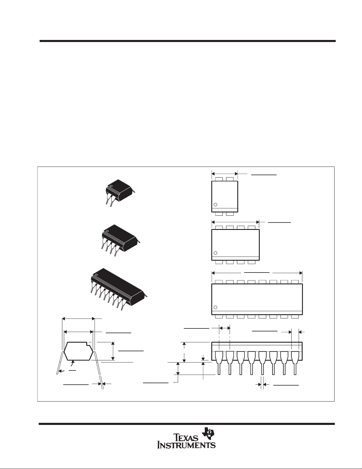
mechanical data
4,80 (0.189)
4,19 (0.165)
TIL920
1
10,2 (0.400)
9,2 (0.362)
TIL921
TIL922
C
105°
°
90
0,36 (0.014)
0,20 (0.008)
NOTE A: Each pin centerline is located 0,25 (0.010) of its true longitudinal position.
C
LL
7,62 (0.300) T.P.
(see Note A)
6,76 (0.266)
6,25 (0.246)
3,81 (0.150)
3,30 (0.130)
Seating Plane
3,81 (0.150)
2,54 (0.100)
ALL LINEAR DIMENSIONS ARE IN MILLIMETERS AND PARENTHETICALLY IN INCHES
5,08 (0.200) MAX
2,79 (0.110)
2,29 (0.090)
(see Note A)
0,51 (0.020) MIN
1
21,1 (0.831)
18,5 (0.728)
1
1,27 (0.050)
1,12 (0.044)
0,58 (0.023)
0,43 (0.017)
PRODUCTION DATA information is current as of publication date.
Products conform to specifications per the terms of Texas Instruments
standard warranty. Production processing does not necessarily include
testing of all parameters.
POST OFFICE BOX 655303 • DALLAS, TEXAS 75265
Copyright 1992, Texas Instruments Incorporated
1
Page 2
TIL920, TIL921, TIL922, TIL920A, TIL921A, TIL922A
TIL920B, TIL921B, TIL922B
SINGLE/DUAL/QUAD CHANNEL OPTOCOUPLERS
SOOS032–D3908, FEBRUARY 1992
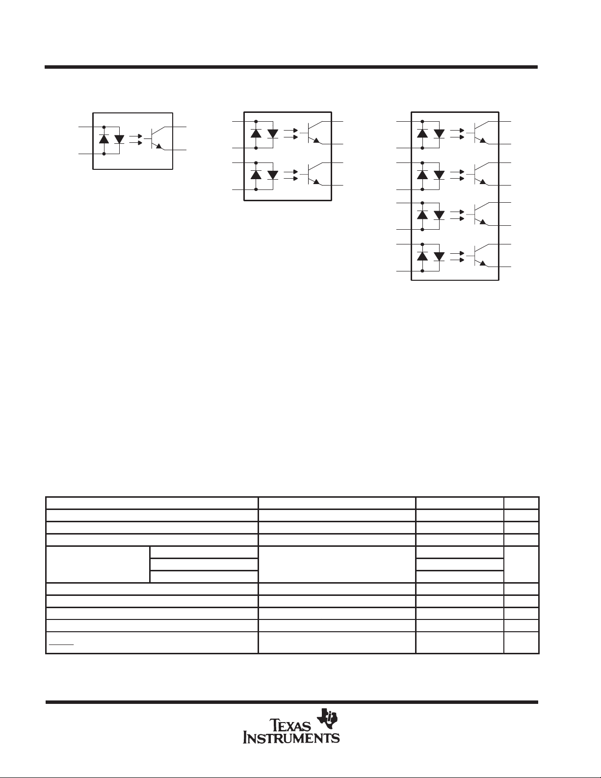
schematic diagrams
A/K
K/A
1
2
TIL920
(TOP VIEW)
4
C
3
E
1 A/K
1 K/A
2 A/K
2 K/A
1
2
3
4
TIL921
(TOP VIEW)
TIL922
(TOP VIEW)
8
1C
7
1E
6
2C
5
2E
1A/K
1K/A
2A/K
2K/A
3A/K
3K/A
4A/K
4K/A
1
2
3
4
5
6
7
8
16
15
14
13
12
11
10
1C
1E
2C
2E
3C
3E
4C
9
4E
absolute maximum ratings, T
= 25°C (unless otherwise noted)
A
Input-to-output voltage (see Note 1) ±7.5 kV peak or dc (±5.3 kV rms). . . . . . . . . . . . . . . . . . . . . . . . . . . . . . . .
Collector-emitter voltage (see Note 2) 35 V. . . . . . . . . . . . . . . . . . . . . . . . . . . . . . . . . . . . . . . . . . . . . . . . . . . . . . .
Emitter-collector voltage 7 V. . . . . . . . . . . . . . . . . . . . . . . . . . . . . . . . . . . . . . . . . . . . . . . . . . . . . . . . . . . . . . . . . . . . .
Input diode continuous forward current at (or below) 25°C free-air temperature (see Note 3) ±50 mA. . . . .
Continuous power dissipation at (or below) 25°C free-air temperature:
Phototransistor (see Note 4) 150 mW. . . . . . . . . . . . . . . . . . . . . . . . . . . . . . . . . . . . . . . . . . . . . . . . . . . . . . . .
Input diode plus phototransistor per channel (see Note 5) 200 mW. . . . . . . . . . . . . . . . . . . . . . . . . . . . . .
Operating free-air temperature range, T
–55°C to 100°C. . . . . . . . . . . . . . . . . . . . . . . . . . . . . . . . . . . . . . . . . .
A
Storage temperature range –55°C to 125°C. . . . . . . . . . . . . . . . . . . . . . . . . . . . . . . . . . . . . . . . . . . . . . . . . . . . . . .
Lead temperature 1,6 mm (1/16 inch) from case for 10 seconds 260°C. . . . . . . . . . . . . . . . . . . . . . . . . . . . . . .
NOTES: 1. This rating applies for sine-wave operation at 50 or 60 Hz. Service capability is verified by testing in accordance with UL requirements.
electrical characteristics, T
†
NOTES: 6. These parameters are measured between all input-diode leads shorted together and all phototransistor leads shorted together.
2. This value applies when the base-emitter diode is open circuited.
3. Derate linearly to 100°C free-air temperature at the rate of 0.67 mA/°C.
4. Derate linearly to 100°C free-air temperature at the rate of 2 mW/°C.
5. Derate linearly to 100°C free-air temperature at the rate of 2.67 mW/°C.
= 25°C (unless otherwise noted)
A
PARAMETER TEST CONDITIONS MIN TYP MAX UNIT
V
(BR)CEO
V
(BR)ECO
I
C(off)
†
CTR
†
V
F
V
CE(sat)
C
io
r
io
I
C(on)1
I
C(on)2
These parameters apply to either direction of the input current.
Collector-emitter breakdown voltage IC = 0.5 mA, IF = 0 35 V
Emitter-collector breakdown voltage IC = 100 µA, IF = 0 7 V
Off-state collector current VCE = 24 V, IF = 0 100 nA
Current TIL920, TIL921, TIL922 20%
transfer TIL920A, TIL921A, TIL922A IF = 5 mA, VCE = 5 V 50%
ratio TIL920B, TIL921B, TIL922B 100%
Input diode static forward voltage IF = 20 mA 1.4 V
†
Collector-emitter saturation voltage IF = 5 mA, IC = 1 mA 0.4 V
Input-to-output capacitance V
Input-to-output internal resistance V
On-state collector current symmetry ratio
(see Note 7)
7. The higher of the two values of I
generated by the two diodes is taken as I
C(on)
in-out
in-out
VCE = 5 V, IF = 5 mA 1 3
= 0, f = 1 MHz, See Note 6 1 pF
= ±1 kV, See Note 6 10
.
C(on)1
11
Ω
2
POST OFFICE BOX 655303 • DALLAS, TEXAS 75265
Page 3

TIL920, TIL921, TIL922, TIL920A, TIL921A, TIL922A
TIL920B, TIL921B, TIL922B
SINGLE/DUAL/QUAD CHANNEL OPTOCOUPLERS
SOOS032–D3908, FEBRUARY 1992
switching characteristics, T
PARAMETER
t
Rise time 6
r
t
Fall time 6
f
†
These parameters apply to either direction of the input current.
= 25°C
A
†
VCC = 5 V, I
TEST CONDITIONS TYP UNIT
= 2 mA, RL = 100 Ω, See Figure 1
C(on)
PARAMETER MEASUREMENT INFORMATION
Adjust amplitude of input pulse for I
Input
47 Ω
+
VCC = 5 V
–
TEST CIRCUIT VOLTAGE WAVEFORMS
NOTES: A. The input waveform is supplied by a generator with the following characteristics: Zo = 50 Ω, tr ≤ 15 ns, duty cycle = 1%.
B. The output waveform is monitored on an oscilloscope with the following characteristics: tr ≤ 12 ns, Ri ≥ 1 MΩ, Ci ≤ 20 pF.
Input
(see Note A)
Output
(see Note B)
RL = 100 Ω
0
t
r
Output
0
90%
10%
Figure 1. Switching Times
C(on)
= 2 mA
t
f
90%
10%
10%
90%
t
f
t
r
90%
10%
µs
TYPICAL CHARACTERISTICS
100
TA = 25°C
80
60
40
20
0
–20
– Input Current – mA
–40
F
I
–60
–80
–100
–1.6 –1.2 –0.8 –0.4
INPUT CURRENT
vs
INPUT VOLTAGE
0 0.4 0.8
VF – Input Voltage – V
Figure 2
1.2 1.6
POST OFFICE BOX 655303 • DALLAS, TEXAS 75265
3
Page 4

TIL920, TIL921, TIL922, TIL920A, TIL921A, TIL922A
A
TIL920B, TIL921B, TIL922B
SINGLE/DUAL/QUAD CHANNEL OPTOCOUPLERS
SOOS032–D3908, FEBRUARY 1992
TYPICAL CHARACTERISTICS
COLLECTOR CURRENT
vs
COLLECTOR-EMITTER VOLTAGE
20
TA = 25°C
18
16
14
12
10
8
6
– Collector Current – mA
C
I
4
2
0
0123456
VCE – Collector-Emitter Voltage – V
78910
Figure 3 Figure 4
RELATIVE ON-STATE COLLECTOR CURRENT
vs
FREE-AIR TEMPERATURE
1.4
C
°
1.3
1.2
A
T
1.1
1.0
VCE = 5 V
IF = 5 mA
IF = 12 mA
IF = 10 mA
IF = 8 mA
IF = 5 mA
IF = 2 mA
NORMALIZED ON-STATE COLLECTOR
CURRENT
vs
100
40
10
0.4
0.1
0.04
– Normalized Collector Current
0.01
C(on)
I
0.004
0.001
INPUT-DIODE FORWARD CURRENT
VCE = 5 V
Normalized to IF = 5 mA
TA = 25°C
4
1
0.1 0.4 1 4 10 40
IF – Input Current – mA
TYPICAL COLLECTOR-EMITTER SATURATION VOLT
vs
FREE-AIR TEMPERATURE
0.40
IF = 5 mA
0.35
0.30
0.25
IC = 1 mA
100
0.9
0.8
0.7
0.6
0.5
Collector Current Relative to Value at = 25
0.4
–75 –50 –25 0 25 50 100
TA – Free-Air Temperature – ° C
Figure 5 Figure 6
4
0.20
0.15
0.10
– Clooector-Emitter Saturation Voltage – V
0.05
CE(sat)
0
V
75
POST OFFICE BOX 655303 • DALLAS, TEXAS 75265
–75 –50 –25 0 25 50 10075
TA – Free-Air Temperature – ° C
Page 5

IMPORTANT NOTICE
T exas Instruments and its subsidiaries (TI) reserve the right to make changes to their products or to discontinue
any product or service without notice, and advise customers to obtain the latest version of relevant information
to verify, before placing orders, that information being relied on is current and complete. All products are sold
subject to the terms and conditions of sale supplied at the time of order acknowledgement, including those
pertaining to warranty, patent infringement, and limitation of liability.
TI warrants performance of its semiconductor products to the specifications applicable at the time of sale in
accordance with TI’s standard warranty. Testing and other quality control techniques are utilized to the extent
TI deems necessary to support this warranty . Specific testing of all parameters of each device is not necessarily
performed, except those mandated by government requirements.
CERT AIN APPLICATIONS USING SEMICONDUCTOR PRODUCTS MAY INVOLVE POTENTIAL RISKS OF
DEATH, PERSONAL INJURY, OR SEVERE PROPERTY OR ENVIRONMENTAL DAMAGE (“CRITICAL
APPLICATIONS”). TI SEMICONDUCTOR PRODUCTS ARE NOT DESIGNED, AUTHORIZED, OR
WARRANTED TO BE SUITABLE FOR USE IN LIFE-SUPPORT DEVICES OR SYSTEMS OR OTHER
CRITICAL APPLICA TIONS. INCLUSION OF TI PRODUCTS IN SUCH APPLICATIONS IS UNDERST OOD TO
BE FULLY AT THE CUSTOMER’S RISK.
In order to minimize risks associated with the customer’s applications, adequate design and operating
safeguards must be provided by the customer to minimize inherent or procedural hazards.
TI assumes no liability for applications assistance or customer product design. TI does not warrant or represent
that any license, either express or implied, is granted under any patent right, copyright, mask work right, or other
intellectual property right of TI covering or relating to any combination, machine, or process in which such
semiconductor products or services might be or are used. TI’s publication of information regarding any third
party’s products or services does not constitute TI’s approval, warranty or endorsement thereof.
Copyright 1998, Texas Instruments Incorporated
 Loading...