

Page 1
TIDA-00642 Foot controller Using Analog Hall Sensor
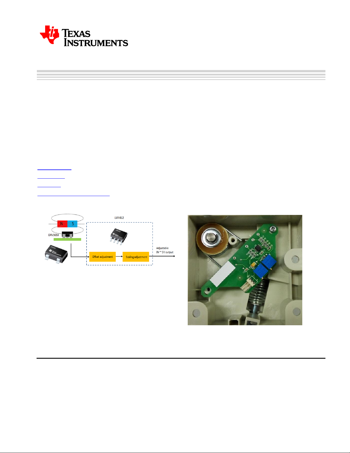
Design Overview
TIDA-00642 uses analog Hall Sensor DRV5053
and OpAmp LMV612 to achieve a foot controller
circuit with approximate linear response and
adjustable quiescent offset and the full scale
output range.
Design Resources
0 to 5V full scale output ability
Adjustable quiescent offset voltage at
zero magnet field
Adjustable wide range system sensitivity
Low power RRIO amplifier stage
Cost effective
Featured Applications
TIDA-00642 Design Folder
DRV5053 Product Folder
LMV612 Product Folder
OpAmp Application Guide
Design Features
Approximate linear response of the
position to output voltage
Adapt with wide magnet types and range
of flux density
Foot controller
Industrial control stick
Industrial foot pedal
Key stroke monitor
General position or angular sensing
1. Introduction
Analog Hall sensor can be used as position or angular sensing with the benefits of no contact and
wearing, high stability and repeat positioning accuracy and wide sensibility range. There are normally
two major methods of the configuration of the magnet and the Hall senor, non-linear and linear way.
This design gives introduction of the two methods and focuses on the linear configuration, and gives
OpAmp circuit design to achieve wide adaption to different applications.
1
Page 2
TIDA-00642 Foot controller Using Analog Hall Sensor
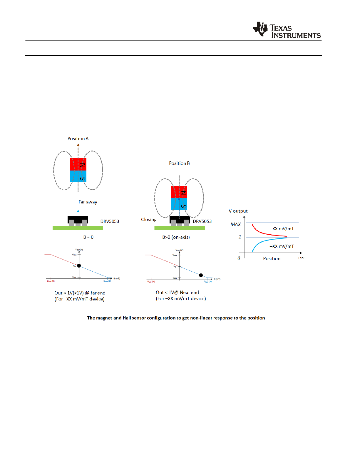
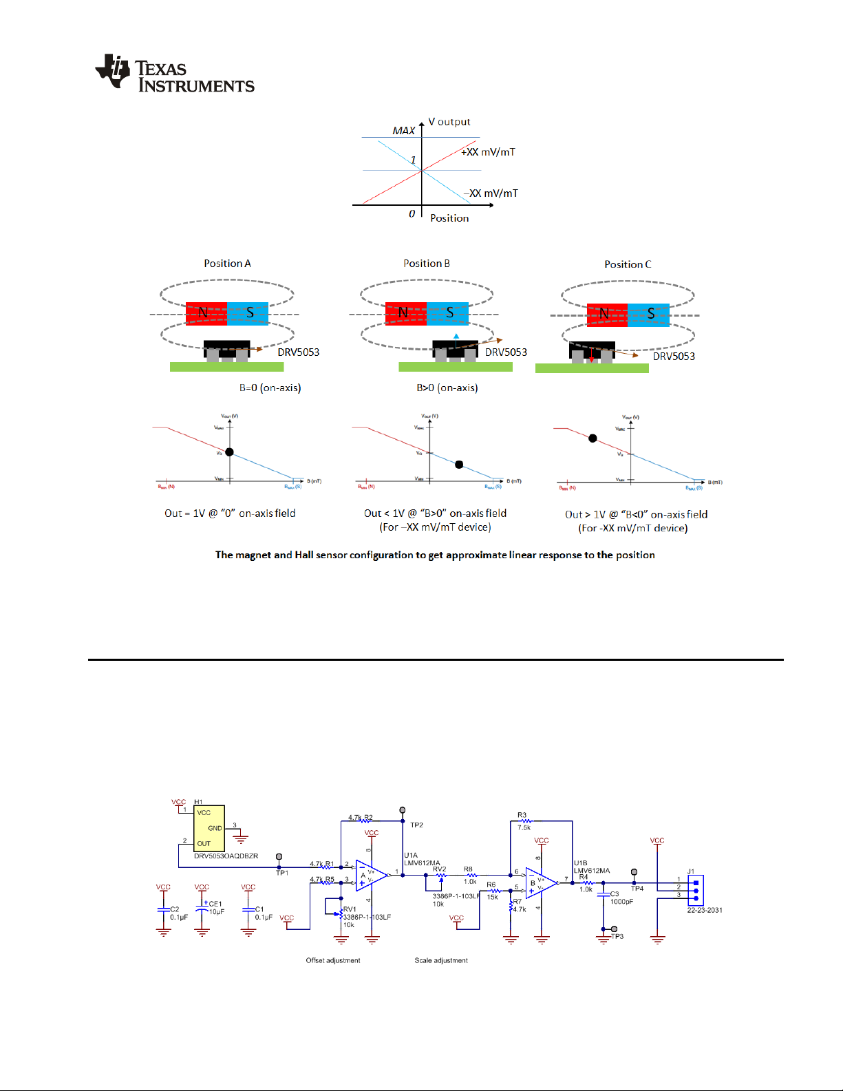
2. Magnet Configuration
The following figures show the two configurations of the magnet and Hall sensor. In non-linear way, the
magnet is approaching the Hall sensor with one of its pole. The output is non-linear to the approaching
distance. In linear configuration, the Hall sensor is placed at the mid position of the magnet as the
quiescent position, no perpendicular flux through the Hall sensor. When the magnet departs from the
quiescent position, the output can change two-way up or down depending on the moving direction.
With the help of OpAmp stage, both the two configurations can output 0 to 5V continual analog signal.
Please refer to Figure 1 and Figure 2 for the two configurations.
2
Figure 1. Non-linear magnet configuration
Page 3
TIDA-00642 Foot controller Using Analog Hall Sensor
Figure 2. Linear magnet configuration
3. OpAmp Circuit
The output of DRV5053 is about 0.2V to 1.8V with the quiescent 1V at zero field or no perpendicular
flux to the sensing surface. In non-linear configuration, the output range is limited either from 0.2V to
1V or from 1V to 1.8V. An OpAmp stage is introduced in this design. It deals with the raw Hall sensor
output signal with adjustable offset and scaling range, shown in Figure 3.
Figure 3. OpAmp stage
3
Page 4

TIDA-00642 Foot controller Using Analog Hall Sensor
S
N
Hall Senor
on the back
Up stroke
Down
stroke
Balance
position
A low cost low power RRIO OpAmp LMV612 is used for the condition circuit. U1A is used for offset
adjustment. The offset is not defined as only to the quiescent point of DRV5053. Actually any fixed
position along the full stroke of the magnet can be set as offset point mechanically. When the relative
position of the magnet and Hall sensor is fixed at the designed offset point, the final output voltage can
be adjustment by RV1. U1B is used as the amplitude amplifier stage with adjustable gain tuning by
RV2. Also there is a RC filter at the final output with R4 and C3.
Basic tuning guide of the system:
1. Tuning RV1 for the designed fixed offset output
2. Place the magnet to its MIN MAX stroke and tuning RV2 to get designed output range
3. Release or return the fixed offset point, back to step 1 readjustment the offset point
4. Back to step 2 to readjustment the offset output
5. Repeat 1 to 4 steps to get both the designed offset the scaled output range.
6. Note that the adjustment range of offset and scaling is also related to the mechanical magnet
configuration and the magnetic field. Do possible adjustment of the mechanical configuration if
needed.
7. The OpAmp parameters are also adjustable for special sensing range and output coverage. It is
recommend to change R5 for extend offset adjustment ability and R3 for extend gain range.
For the detail design and analysis of the OpAmp circuit, please refer to the following application guide.
http://www.ti.com/lit/an/snla140b/snla140b.pdf
4. Lab Test Data
The following lab test data is done in a typical sew machine foot controller. The following figure shows
the mechanical configuration of the controller box. It is configured in linear way.
Figure 4. Foot pedal structure
4
Page 5

TIDA-00642 Foot controller Using Analog Hall Sensor
The actuator is fixed at a mid-point between the two ends of the stroke by a dual-spring system.
Controlling by the foot, the actuator can go two sides of the stroke direction. The application requires
the output stay at about 1.1V when the actuator is at the balanced point (fixed offset point). When the
foot strokes downside, the output goes from 1.1V down to ~0V. When the foot strokes upside, the
output goes from 1.1V up to ~5V (VCC). This 0 to 5V analog signal will output to the sewing machine
control unit and be taken as the speed commands of the spindle.
Below figure shows the output voltage test data.
(a) Up stroke
5
Page 6

TIDA-00642 Foot controller Using Analog Hall Sensor
(b) Down stoke
Figure 5. Output test data example
6
Page 7

IMPORTANT NOTICE FOR TI REFERENCE DESIGNS
Texas Instruments Incorporated ("TI") reference designs are solely intended to assist designers (“Buyers”) who are developing systems that
incorporate TI semiconductor products (also referred to herein as “components”). Buyer understands and agrees that Buyer remains
responsible for using its independent analysis, evaluation and judgment in designing Buyer’s systems and products.
TI reference designs have been created using standard laboratory conditions and engineering practices. TI has not conducted any
testing other than that specifically described in the published documentation for a particular reference design. TI may make
corrections, enhancements, improvements and other changes to its reference designs.
Buyers are authorized to use TI reference designs with the TI component(s) identified in each particular reference design and to modify the
reference design in the development of their end products. HOWEVER, NO OTHER LICENSE, EXPRESS OR IMPLIED, BY ESTOPPEL
OR OTHERWISE TO ANY OTHER TI INTELLECTUAL PROPERTY RIGHT, AND NO LICENSE TO ANY THIRD PARTY TECHNOLOGY
OR INTELLECTUAL PROPERTY RIGHT, IS GRANTED HEREIN, including but not limited to any patent right, copyright, mask work right,
or other intellectual property right relating to any combination, machine, or process in which TI components or services are used.
Information published by TI regarding third-party products or services does not constitute a license to use such products or services, or a
warranty or endorsement thereof. Use of such information may require a license from a third party under the patents or other intellectual
property of the third party, or a license from TI under the patents or other intellectual property of TI.
TI REFERENCE DESIGNS ARE PROVIDED "AS IS". TI MAKES NO WARRANTIES OR REPRESENTATIONS WITH REGARD TO THE
REFERENCE DESIGNS OR USE OF THE REFERENCE DESIGNS, EXPRESS, IMPLIED OR STATUTORY, INCLUDING ACCURACY OR
COMPLETENESS. TI DISCLAIMS ANY WARRANTY OF TITLE AND ANY IMPLIED WARRANTIES OF MERCHANTABILITY, FITNESS
FOR A PARTICULAR PURPOSE, QUIET ENJOYMENT, QUIET POSSESSION, AND NON-INFRINGEMENT OF ANY THIRD PARTY
INTELLECTUAL PROPERTY RIGHTS WITH REGARD TO TI REFERENCE DESIGNS OR USE THEREOF. TI SHALL NOT BE LIABLE
FOR AND SHALL NOT DEFEND OR INDEMNIFY BUYERS AGAINST ANY THIRD PARTY INFRINGEMENT CLAIM THAT RELATES TO
OR IS BASED ON A COMBINATION OF COMPONENTS PROVIDED IN A TI REFERENCE DESIGN. IN NO EVENT SHALL TI BE
LIABLE FOR ANY ACTUAL, SPECIAL, INCIDENTAL, CONSEQUENTIAL OR INDIRECT DAMAGES, HOWEVER CAUSED, ON ANY
THEORY OF LIABILITY AND WHETHER OR NOT TI HAS BEEN ADVISED OF THE POSSIBILITY OF SUCH DAMAGES, ARISING IN
ANY WAY OUT OF TI REFERENCE DESIGNS OR BUYER’S USE OF TI REFERENCE DESIGNS.
TI reserves the right to make corrections, enhancements, improvements and other changes to its semiconductor products and services per
JESD46, latest issue, and to discontinue any product or service per JESD48, latest issue. Buyers should obtain the latest relevant
information before placing orders and should verify that such information is current and complete. All semiconductor products are sold
subject to TI’s terms and conditions of sale supplied at the time of order acknowledgment.
TI warrants performance of its components to the specifications applicable at the time of sale, in accordance with the warranty in TI’s terms
and conditions of sale of semiconductor products. Testing and other quality control techniques for TI components are used to the extent TI
deems necessary to support this warranty. Except where mandated by applicable law, testing of all parameters of each component is not
necessarily performed.
TI assumes no liability for applications assistance or the design of Buyers’ products. Buyers are responsible for their products and
applications using TI components. To minimize the risks associated with Buyers’ products and applications, Buyers should provide
adequate design and operating safeguards.
Reproduction of significant portions of TI information in TI data books, data sheets or reference designs is permissible only if reproduction is
without alteration and is accompanied by all associated warranties, conditions, limitations, and notices. TI is not responsible or liable for
such altered documentation. Information of third parties may be subject to additional restrictions.
Buyer acknowledges and agrees that it is solely responsible for compliance with all legal, regulatory and safety-related requirements
concerning its products, and any use of TI components in its applications, notwithstanding any applications-related information or support
that may be provided by TI. Buyer represents and agrees that it has all the necessary expertise to create and implement safeguards that
anticipate dangerous failures, monitor failures and their consequences, lessen the likelihood of dangerous failures and take appropriate
remedial actions. Buyer will fully indemnify TI and its representatives against any damages arising out of the use of any TI components in
Buyer’s safety-critical applications.
In some cases, TI components may be promoted specifically to facilitate safety-related applications. With such components, TI’s goal is to
help enable customers to design and create their own end-product solutions that meet applicable functional safety standards and
requirements. Nonetheless, such components are subject to these terms.
No TI components are authorized for use in FDA Class III (or similar life-critical medical equipment) unless authorized officers of the parties
have executed an agreement specifically governing such use.
Only those TI components that TI has specifically designated as military grade or “enhanced plastic” are designed and intended for use in
military/aerospace applications or environments. Buyer acknowledges and agrees that any military or aerospace use of TI components that
have not been so designated is solely at Buyer's risk, and Buyer is solely responsible for compliance with all legal and regulatory
requirements in connection with such use.
TI has specifically designated certain components as meeting ISO/TS16949 requirements, mainly for automotive use. In any case of use of
non-designated products, TI will not be responsible for any failure to meet ISO/TS16949.IMPORTANT NOTICE
Mailing Address: Texas Instruments, Post Office Box 655303, Dallas, Texas 75265
Copyright © 2015, Texas Instruments Incorporated
 Loading...