

Texas Instruments TCM320AC36CPT, TCM320AC36CN, TCM320AC36CDW, TCM320AC36CDWR, TCM320AC37IDW Datasheet
...
D
Single 5-V Operation
D
Low Power Consumption:
– Operating Mode...40 mW Typ
– Standby Mode... 5 mW Typ
– Power-Down Mode...3 mW Typ
D
Combined A/D, D/A, and Filters
D
Extended Variable-Frequency Operation
– Sample Rates up to 16 kHz
– Pass-Band up to 7.2 kHz
D
Electret Microphone Bias Reference
Voltage Available
D
Drive a Piezo Speaker Directly
D
Compatible With All Digital Signal
Processors (DSPs)
TCM320AC36, TCM320AC37
VOICE-BAND AUDIO PROCESSORS (VBAP)
SLWS003C – MAY 1992 – REVISED APRIL – 1998
D
Selectable Between 8-Bit Companded and
13-Bit (Dynamic Range) Linear Conversion:
– TCM320AC36 . . . µ-Law and Linear
Modes
– TCM320AC37...A-Law and Linear
Modes
D
Programmable Volume Control in Linear
Mode
D
300 Hz – 3.6 kHz Passband with Specified
Master Clock
D
Designed for Standard 2.048-MHz Master
Clock for U.S. Analog, U.S. Digital, CT2,
DECT, GSM, and PCS Standards for
Hand-Held Battery-Powered Telephones
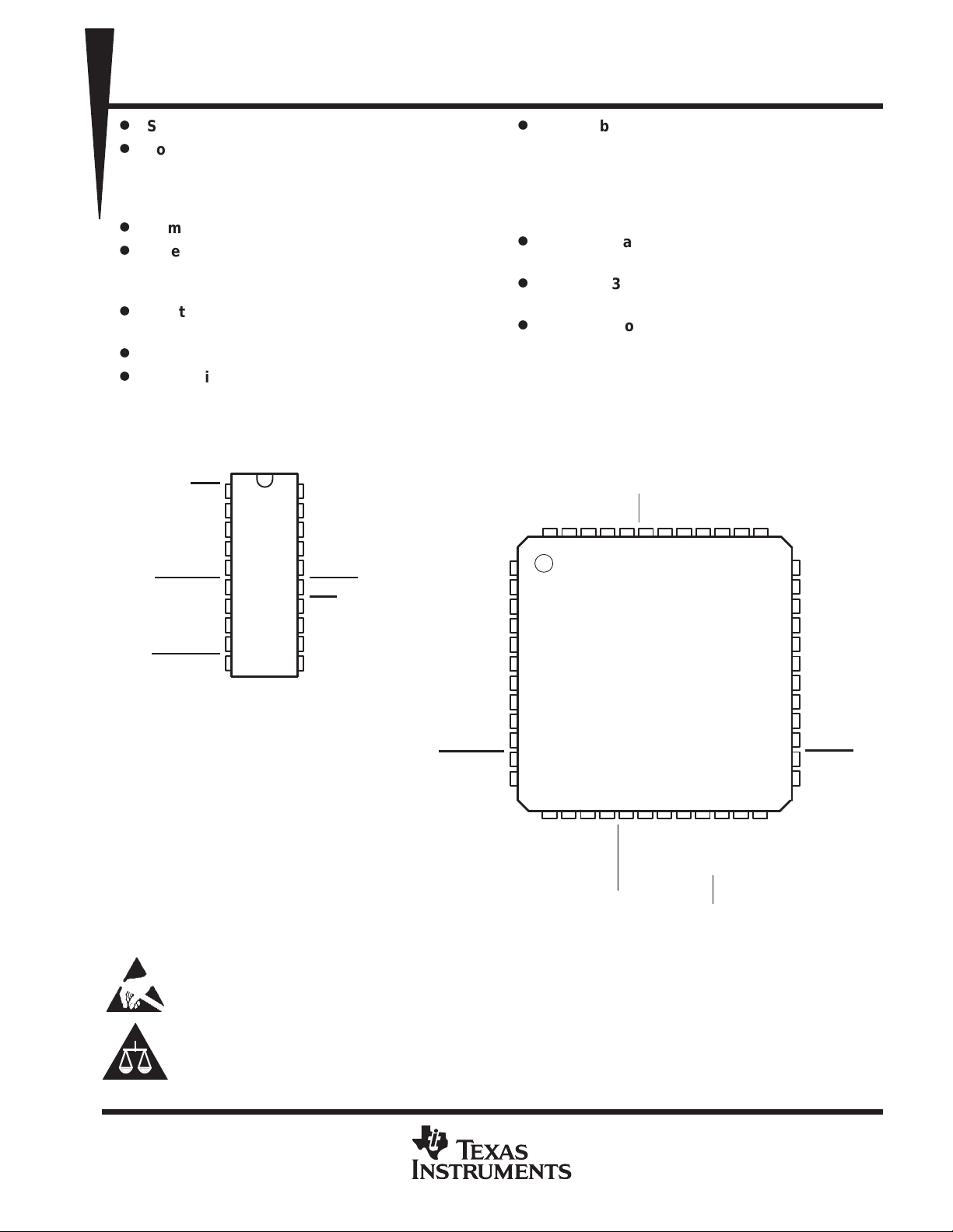
DW OR N PACKAGE
PDN
EARA
EARB
EARGS
V
CC
MICMUTE
DCLKR
DIN
FSR
EARMUTE
(TOP VIEW)
1
20
2
19
3
18
4
17
5
16
6
15
7
14
8
13
9
12
10
11
MICBIAS
MICGS
MICIN
VMID
GND
LINSEL
TSX/DCLKX
DOUT
FSX
CLK
NCNCEARGS
47 46 45 44 4348 42
NC
1
NC
2
NC
3
CC
NC
NC
NC
NC
CC
NC
NC
4
5
6
7
8
9
10
11
12
13
14 15
AV
DV
MICMUTE
NC
DCLKR
NC – No internal connection
PT PACKAGE
(TOP VIEW)
EARB
EARA
17 18 19 20
16
DIN
FSR
EARMUTE
PDN
MICBIAS
NC
CLK
MICGS
MICINNCNC
40 39 3841
21
22 23 24
FSX
DOUT
NC
37
36
35
34
33
32
31
30
29
28
27
26
25
NC
NC
TSX/DCLKX
VMID
NC
AGND
NC
NC
NC
NC
NC
NC
DGND
LINSEL
NC
These devices have limited built-in ESD protection. The leads should be shorted together or the device placed in conductive foam
during storage or handling to prevent electrostatic damage to the MOS gates.
Please be aware that an important notice concerning availability, standard warranty, and use in critical applications of
Texas Instruments semiconductor products and disclaimers thereto appears at the end of this data sheet.
VBAP is a trademark of Texas Instruments Incorporated.
PRODUCTION DATA information is current as of publication date.
Products conform to specifications per the terms of Texas Instruments
standard warranty. Production processing does not necessarily include
testing of all parameters.
POST OFFICE BOX 655303 • DALLAS, TEXAS 75265
Copyright 1998, Texas Instruments Incorporated
1

TCM320AC36, TCM320AC37
VOICE-BAND AUDIO PROCESSORS (VBAP)
SLWS003C – MAY 1992 – REVISED APRIL – 1998
description
The TCM320AC36 and TCM320AC37 voice-band audio processor (VBAP) integrated circuits are designed to
perform the transmit encoding (A/D conversion) and receive decoding (D/A conversion) together with transmit
and receive filtering for voice-band communications systems. Cellular telephone systems are targeted in
particular; however, these integrated circuits can function in other systems including digital audio,
telecommunications, and data acquisition.
These devices are pin-selectable for either of two modes, companded and linear, providing data in two formats.
In the companded mode, data is transmitted and received in 8-bit words. In the linear mode, 13 bits of data, and
either three bits of gain-setting control data, or three zero bits of padding to create a 16-bit word, are sent and
received.
The transmit section is designed to interface directly with an electret microphone element. The microphone input
signal (MICIN) is buffered and amplified, with provision for setting the amplifier gain to accommodate a range
of signal input levels. The amplified signal is passed through antialiasing and band-pass filters. The filtered
signal is then applied to the input of a compressing analog-to-digital converter (COADC) when companded
mode is selected. Otherwise, the analog-to-digital converter performs a linear conversion. The resulting data
is then clocked out of DOUT as a serial data stream.
The receive section takes a frame of serial data on DIN and converts it to analog through an expanding
digital-to-analog converter (EXDAC) when the companded mode is selected; otherwise, a linear conversion is
performed. The analog signal then passes through switched capacitor filters, which provide out-of-band
rejection, (sin x)/x correction functions, and smoothing. The filtered signal is sent to the earphone amplifier. The
earphone amplifier has a differential output with adjustable gain and is designed to minimize static power
dissipation.
A single on-chip high-precision band-gap circuit generates all voltage references, eliminating the need for
external reference voltages. An internal reference voltage equal to V
virtual ground for all the amplifier circuits and the microphone bias circuit. Another reference voltage, MICBIAS,
can supply bias current for the microphone.
The TCM320AC3xC devices are characterized for operation from 0°C to 70°C. The TCM320AC3xI devices are
characterized for operation from –40°C to 85°C.
/2, VMID, is used to develop the midlevel
CC
2
POST OFFICE BOX 655303 • DALLAS, TEXAS 75265
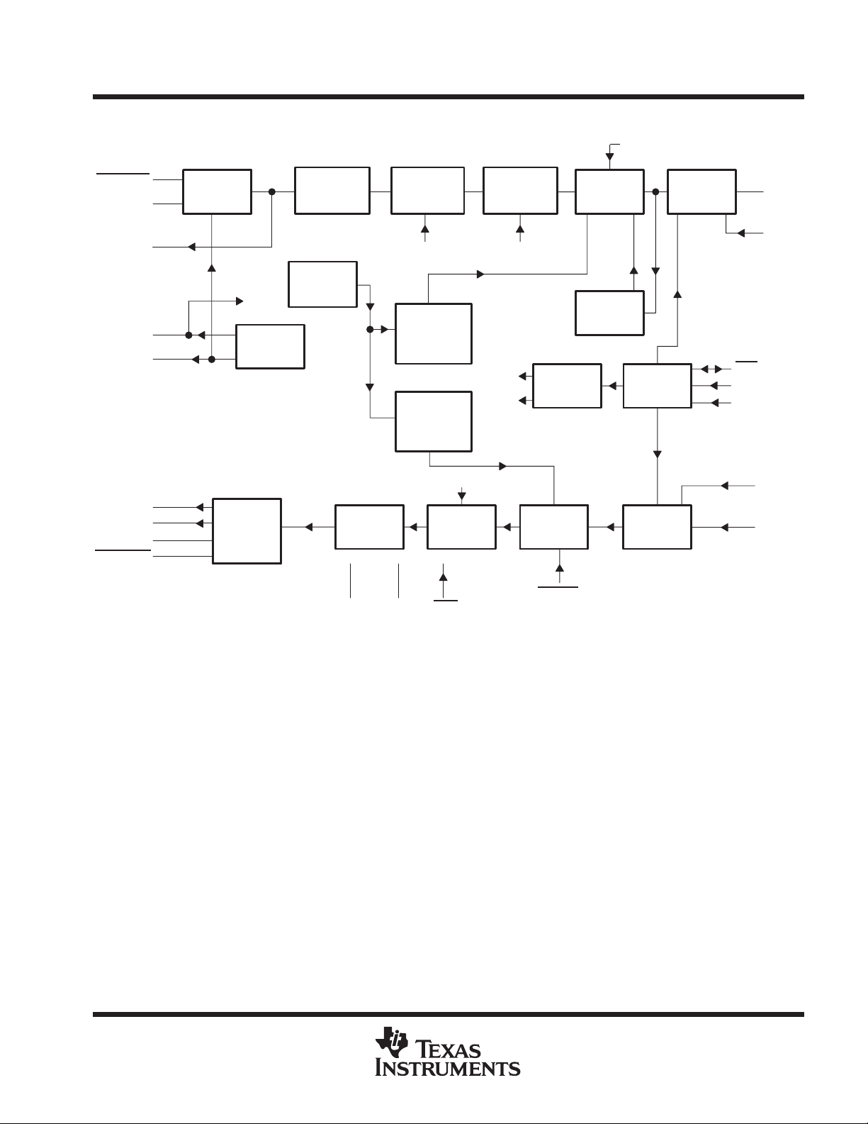
functional block diagram
VMID
6
18
19
17
20
Input
Buffer
VMID
VMID
Generator
MICMUTE
MICIN
MICGS
MICBIAS
Transmit
Third-Order
Antialias
Band-Gap
Voltage
Reference
VOICE-BAND AUDIO PROCESSORS (VBAP)
Transmit
Sixth-Order
Low Pass
256 kHz 8 kHz
A/D
Converter
Voltage
Reference
D/A
Converter
Voltage
Reference
Transmit
First-Order
High Pass
256 kHz
8 kHz
TCM320AC36, TCM320AC37
SLWS003C – MAY 1992 – REVISED APRIL – 1998
LINSEL
15
Output
Logic
Clock
Clock
Generator
ADC
Autozero
Control
14
11
7
13
12
TSX
/DCLKX
CLK
DCLKR
DOUT
FSX
EARA
EARB
EARGS
EARMUTE
Terminal numbers shown are for the DW and N packages.
2
3
4
10
Earphone
Amplifier
Receive
V
CC
Buffer
5
GND
16
256 kHz
Receive
Filter
1
PDN
DAC
15
LINSEL
Input
Logic
9
FSR
8
DIN
POST OFFICE BOX 655303 • DALLAS, TEXAS 75265
3
TCM320AC36, TCM320AC37
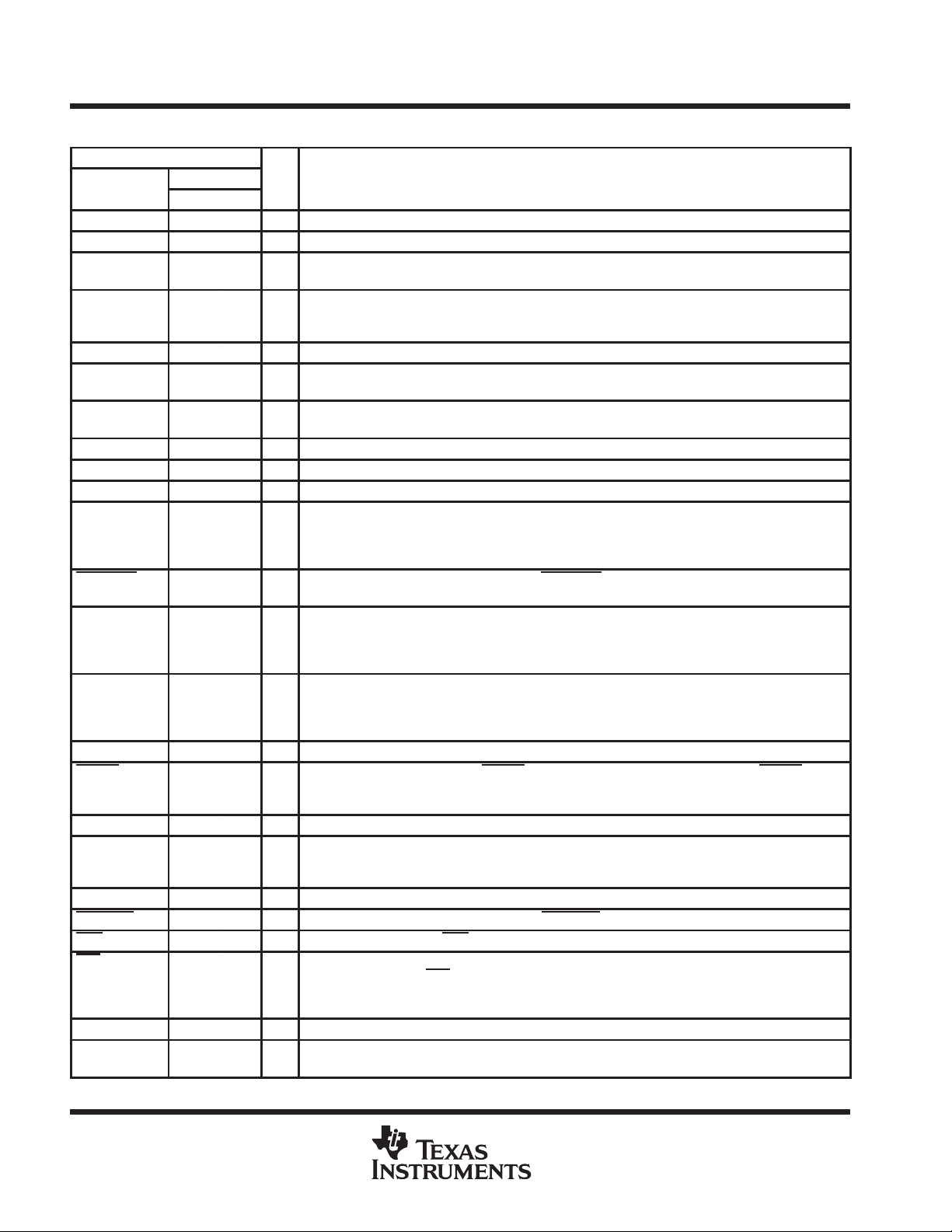
NAME
VOICE-BAND AUDIO PROCESSORS (VBAP)
SLWS003C – MAY 1992 – REVISED APRIL – 1998
Terminal Functions
TERMINAL
NO.
DW, N PT
AGND — 34 Ground return for all internal analog circuits
AV
CC
CLK 11 19 I Clock input. In the fixed-data-rate mode, CLK is the master clock input as well as the transmit and
DCLKR 7 14 I Selection of fixed- or variable-data-rate operation. When DCLKR is connected to VCC, the device
DGND — 27 Ground return for all internal digital circuits
DIN 8 15 I Receive data input. Input data is clocked in on consecutive negative transitions of the receive data
DOUT 13 21 O Transmit data output. Transmit data is clocked out on consecutive positive transitions of the transmit
DV
CC
EARA 2 44 O Earphone output. EARA forms a differential drive when used with the EARB signal (analog).
EARB 3 45 O Earphone output. EARB forms a differential drive when used with the EARA signal (analog).
EARGS 4 46 I Earphone gain set input of feedback signal for the earphone output. The ratio of an external potential
EARMUTE 10 17 I Earphone output mute control signal. When EARMUTE is low, the output amplifier is disabled and no
FSR 9 16 I Frame-synchronization clock input for the receive channel. In the variable-data-rate mode, this signal
FSX 12 20 I Frame synchronization clock input for the transmit channel. FSX operates independently of FSR, but
GND 16 — Ground return for all internal circuits
LINSEL 15 26 I Linear selection input. When low, LINSEL selects linear coding/decoding. When high, LINSEL selects
MICBIAS 20 42 O Microphone bias. MICBIAS voltage for the electret microphone is equal to VMID.
MICGS 19 41 O Output of the internal microphone amplifier. MICGS is used as the feedback to set the microphone
MICIN 18 40 I Microphone input. Electret microphone input to the internal microphone amplifier (analog)
MICMUTE 6 11 I Microphone input mute control signal. When MICMUTE is active (low), zero code is transmitted (dig.).
PDN 1 43 I Power-down input. When PDN is low, the device powers down to reduce power consumption (digital).
TSX/DCLKX 14 22 I/O Transmit time slot strobe (active-low output) or data clock (input) for the transmit channel. In the
V
CC
VMID 17 36 O VCC/2 bias voltage reference. A pair of external, low-leakage, high-frequency capacitors (1 µF and
— 4 5-V supply voltage for all internal analog circuits
— 9 5-V supply voltage for all internal digital circuits
5 — 5-V supply voltage for all internal circuits
I/O DESCRIPTION
receive data clock input . In the variable-data-rate mode, CLK is the master clock input only (digital).
operates in the fixed-data-rate mode. When DCLKR is not connected to VCC, the device operates in
the variable-data-rate mode, and DCLKR becomes the receive data clock (digital).
clock, which is CLK for a fixed data rate and DCLKR for a variable data rate (digital).
data clock, which is CLK for a fixed data rate and DCLKX for a variable data rate (digital).
divider network connected across EARA and EARB adjusts the power amplifier gain. Maximum gain
occurs when EARGS is connected to EARB. Minimum gain occurs when EARGS is connected to
EARA. Earphone frequency response correction is performed using an RC approach (analog).
audio is sent to the earphone (digital).
must remain high for the duration of the time slot. The receive channel enters the standby condition
when FSR is TTL-low for five frames or longer. The device enters a production test-mode condition
when either FSR or FSX is held high for five frames or longer (digital).
also in an analogous manner to FSR. The transmit channel enters the standby condition when FSX
is low for five frames or longer. The device enters a production test-mode condition when either FSX
or FSR is held high for five frames or longer (digital).
companded coding/decoding. Companding code on the ’AC36 is µ-law , and companding code on the
’AC37 is A-law (digital).
amplifier gain. If sidetone is required, it is accomplished by connecting a series network between
MICGS and EARGS (analog).
fixed-data-rate mode, TSX
enable signal for a 3-state buffer. In the variable-data-rate mode, DCLKX becomes the transmit data
clock input (digital).
470 pF) should be connected between VMID and ground for filtering.
/DCLKX is an open-drain output that pulls to ground and is used as an
4
POST OFFICE BOX 655303 • DALLAS, TEXAS 75265
Operating free-air temperature, T
°C
TCM320AC36, TCM320AC37
VOICE-BAND AUDIO PROCESSORS (VBAP)
SLWS003C – MAY 1992 – REVISED APRIL – 1998
absolute maximum ratings over operating free-air temperature range (unless otherwise noted)
Supply voltage range, V
Output voltage range at DOUT, V
Input voltage range at DIN, V
(see Note 1) –0.3 V to 7 V. . . . . . . . . . . . . . . . . . . . . . . . . . . . . . . . . . . . . . . . . . . . . .
CC
–0.3 V to 7 V. . . . . . . . . . . . . . . . . . . . . . . . . . . . . . . . . . . . . . . . . . . . . . . . . . .
O
–0.3 V to 7 V. . . . . . . . . . . . . . . . . . . . . . . . . . . . . . . . . . . . . . . . . . . . . . . . . . . . . . .
I
†
Continuous total power dissipation See Dissipation Rating Table. . . . . . . . . . . . . . . . . . . . . . . . . . . . . . . . . . . . .
Operating free-air temperature range: C suffix 0°C to 70°C. . . . . . . . . . . . . . . . . . . . . . . . . . . . . . . . . . . . . . . . .
I suffix –40°C to 85°C. . . . . . . . . . . . . . . . . . . . . . . . . . . . . . . . . . . . . . . .
Storage temperature range, T
–65°C to 150°C. . . . . . . . . . . . . . . . . . . . . . . . . . . . . . . . . . . . . . . . . . . . . . . . . . .
stg
Lead temperature 1,6 mm (1/16 inch) from case for 10 seconds 260°C. . . . . . . . . . . . . . . . . . . . . . . . . . . . . . .
†
Stresses beyond those listed under “absolute maximum ratings” may cause permanent damage to the device. These are stress ratings only, and
functional operation of the device at these or any other conditions beyond those indicated under “recommended operating conditions” is not
implied. Exposure to absolute-maximum-rated conditions for extended periods may affect device reliability.
NOTE 1: Voltage value is with respect to GND.
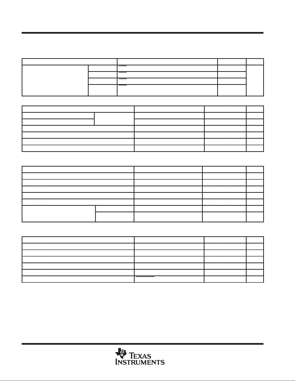
DISSIPATION RATING TABLE
PACKAGE
DW 1025 mW 8.2 mW/° C 656 mW 533 mW
N 1150 mW 9.2 mW/°C 736 mW 598 mW
PT 1075 mW 7.1 mW/°C 756 mW 649 mW
TA ≤ 25°C
POWER RATING
DERATING FACTOR
ABOVE TA = 25°C
TA = 70°C
POWER RATING
TA = 85°C
POWER RATING
recommended operating conditions (see Note 2)
MIN MAX UNIT
Supply voltage, VCC (see Note 3) 4.5 5.5 V
High-level input voltage, V
Low-level input voltage, V
Load resistance between EARA and EARB, RL (see Note 4) 600 Ω
Load capacitance between EARA and EARB, CL (see Note 4) 113 nF
p
NOTES: 2. T o avoid possible damage to these CMOS devices and resulting reliability problems, the power-up sequence detailed in the system
reliability features paragraph should be followed.
3. Voltages at analog inputs, outputs, and VCC are with respect to GND.
4. RL and CL should not be applied simultaneously.
IH
IL
p
A
TCM320AC36C, TCM320AC37C 0 70
TCM320AC36I, TCM320AC37I –40 85
2.2 V
0.8 V
°
POST OFFICE BOX 655303 • DALLAS, TEXAS 75265
5
TCM320AC36, TCM320AC37
DOUT
VOICE-BAND AUDIO PROCESSORS (VBAP)
SLWS003C – MAY 1992 – REVISED APRIL – 1998
electrical characteristics over recommended ranges of supply voltage and free-air temperature
(unless otherwise noted)
supply current, f
I
Supply current from V
CC
DCLKR
PARAMETER TEST CONDITIONS MIN MAX UNIT
or f
DCLKX
CC Standby – both PDN is high with FSX and FSR held low 2
= 2.048 MHz, outputs not loaded, VCC = 5 V, TA = 25°C
Operating PDN is high with CLK signal present 9.9
Power down PDN is low for 500 µs 0.85
Standby – one
PDN is high with either FSX or FSR pulsing with the
other held low
6
digital interface
PARAMETER TEST CONDITIONS MIN TYP†MAX UNIT
V
OH
V
OL
I
IH
I
IL
C
i
C
o
†
All typical values are at VCC = 5 V, TA = 25°C.
High-level output voltage
Low-level output voltage
High-level input current, any digital input VI = 2.2 V to V
Low-level input current, any digital input VI = 0 to 0.8 V 10 µA
Input capacitance 5 pF
Output capacitance 5 pF
IOH = –3.2 mA, VCC = 5 V 2.4 4.6 V
IOL = 3.2 mA, VCC = 5 V 0.2 0.4 V
CC
10 µA
microphone interface
PARAMETER TEST CONDITIONS MIN TYP†MAX UNIT
V
IO
I
IB
B
1
C
i
A
V
IOmax Maximum output current
†
All typical values are at VCC = 5 V, TA = 25°C.
Input offset voltage at MICIN VI = 0 to 5 V ±5 mV
Input bias current at MICIN ±200 nA
Unity-gain bandwidth, open loop at MICIN 1 MHz
Input capacitance at MICIN 5 pF
Large-signal voltage amplification at MICGS 10000 V/V
VMID 1 µA
MICBIAS
(source only)
1 mA
speaker interface
PARAMETER TEST CONDITIONS MIN TYP†MAX UNIT
V
O(PP)
V
OO
I
I(lkg)
IOmax Maximum output current RL = 600 Ω ±5 mA
r
o
†
All typical values are at VCC = 5 V, TA = 25°C.
AC output voltage 3 Vpp
Output offset voltage at EARA, EARB (single-ended) Relative to GND 80 mVpk
Input leakage current at EARGS VI = 0.5 V to (VCC – 0.5) V ±200 nA
Output resistance at EARA, EARB 1 Ω
Gain change EARMUTE low, max level when muted –80 dB
mA
6
POST OFFICE BOX 655303 • DALLAS, TEXAS 75265
dB
Gain error with input level relative to gain at
dBm0
,
Gai
t
In ut am lifier set for unity gain,
1.02 kHz
dB
TCM320AC36, TCM320AC37
VOICE-BAND AUDIO PROCESSORS (VBAP)
SLWS003C – MAY 1992 – REVISED APRIL – 1998
transmit gain and dynamic range, companded mode (µ-law or A-law) or linear mode selected, VCC = 5 V,
T
= 25°C (unless otherwise noted) (see Notes 5 and 6)
A
PARAMETER TEST CONDITIONS MIN MAX UNIT
Companded mode selected, µ-law (’AC36) 0.982
Transmit reference-signal level (0 dB) (see Note 7)
Overload-signal level (MICIN at unity gain)
Absolute gain error 0-dB input signal ±1 dB
p
Gain variation VCC ±10%, TA = 0°C to 70°C ±0.5 dB
NOTES: 5. Unless otherwise noted, the analog input is 0 dB, 1020-Hz sine wave, where 0 dB is defined as the zero-reference point of the channel
under test.
6. The input amplifier is set for inverting unity gain.
7. The reference-signal level, which is input to the transmit channel, is defined as a value 3 dB below the full-scale value of 2 V.
–10
Companded mode selected, A-law (’AC37) 0.985
Linear mode selected (’AC36 and ’AC37) 1.001
Companded mode selected, µ-law (’AC36) 4
Companded mode selected, A-law (’AC37) 4
Linear mode selected (’AC36 and ’AC37) 4
MICIN to DOUT at 3 dBm0 to –36 dBm0 ±0.5
MICIN to DOUT at –37 dBm0 to –40 dBm0 ±1
MICIN to DOUT at –41 dBm0 to –50 dBm0 ±1.5 dB
MICIN to DOUT at –51 dBm0 to –55 dBm0 ±2 dB
Vrms
Vpp
transmit filter transfer, companded mode (µ-law or A-law) or linear mode selected, over recommended
ranges of supply voltage and free-air temperature, CLK = 2.048 MHz, FSX = 8 kHz (see Note 6)
PARAMETER TEST CONDITIONS MIN MAX UNIT
f
= 50 Hz –10 0
MICIN
f
= 200 Hz –1.8 0
MICIN
f
= 300 Hz to 3 kHz ±0.15
n relative to input signal gain a
NOTE 6. The input amplifier is set for inverting unity gain.
Input amplifier set for unity gain
noninverting maximum gain output signal
at MICIN is 0 dB
MICIN
f
= 3.3 kHz –0.35 0.04
MICIN
f
= 3.4 kHz –1 –0.1
MICIN
f
= 4 kHz –14
MICIN
f
≥4.6 kHz –32
MICIN
dB
transmit idle channel noise and distortion, companded mode with µ-law or A-law selected, over
recommended ranges of supply voltage and operating free-air temperature (see Note 8)
PARAMETER TEST CONDITIONS MIN MAX UNIT
Transmit noise, psophometrically weighted MICIN connected to MICGS through a 10-kΩ resistor –71 dB0p
Transmit noise, C-message weighted MICIN connected to MICGS through a 10-kΩ resistor 10 dBrnC0
MICIN to DOUT at 0 dBm0 to –17 dBm0 36
MICIN to DOUT at –18 dBm0 to –23 dBm0 34
Transmit signal-to-distortion ratio with sine-wave input
Intermodulation distortion, 2-tone CCITT method,
composite power level –13 dBm0
NOTE 8: T ransmit noise, linear mode: 200 µVrms is equivalent to –74 dB (referenced to device 0-dB level).
MICIN to DOUT at –24 dBm0 to –29 dBm0 30
MICIN to DOUT at –30 dBm0 to –35 dBm0 24
MICIN to DOUT at –36 dBm0 to –45 dBm0 16
CCITT G.712 (7.1), R2 49
CCITT G.712 (7.2), R3 51
dB
POST OFFICE BOX 655303 • DALLAS, TEXAS 75265
7

TCM320AC36, TCM320AC37
Transmit signal-to-distortion ratio with sine-wave in ut
dB
Gain error with out ut level relative to gain at –10 dBm0
dB
VOICE-BAND AUDIO PROCESSORS (VBAP)
SLWS003C – MAY 1992 – REVISED APRIL – 1998
transmit idle channel noise and distortion, linear mode selected, over recommended ranges of supply
voltage and operating free-air temperature (see Notes 6 and 8)
PARAMETER TEST CONDITIONS MIN MAX UNIT
Transmit noise, C-message weighted MICIN connected to MICGS through a 10-kΩ resistor 200 µVrms
MICIN to DOUT at –6 dBm0 50
MICIN to DOUT at –12 dBm0 48
MICIN to DOUT at –18 dBm0 40
p
MICIN to DOUT at –24 dBm0 35
MICIN to DOUT at –40 dBm0 20
MICIN to DOUT at –45 dBm0 18
NOTES: 6. The input amplifier is set for inverting unity gain.
receive gain and dynamic range, companded mode (µ-law or A-law) or linear mode selected, VCC = 5 V,
T
A
Receive reference-signal level (0 dB) (see Note 11)
Overload-signal level
Absolute gain error 0-dB input signal ±1 dB
Gain variation VCC ±10%, TA = 0°C to 70°C ±0.5 dB
NOTES: 9. Receive output is measured differentially in the maximum gain configuration. T o set the output amplifier for maximum gain, EARGS
8. Transmit noise, linear mode: 200 µVrms is equivalent to –74 dB (referenced to device 0-dB level).
= 25°C (unless otherwise noted) (see Notes 9 and 10)
PARAMETER TEST CONDITIONS MIN MAX UNIT
Companded mode selected, µ-law (’AC36) 0.736
Companded mode selected, A-law (’AC37) 0.739
Linear mode selected (’AC36 and ’AC37) 0.751
Companded mode selected, µ-law (’AC36) 3
Companded mode selected, A-law (’AC37) 3
Linear mode selected (’AC36 and ’AC37) 3
DIN to EARA and EARB at 3 dBm0 to –36 dBm0 ±0.5
p
is connected to EARB and the output is taken between EARA and EARB. All output levels are (sin x)/x corrected.
10. Unless otherwise noted, the digital input is a word stream generated by passing a 0-dB sine wave at 1020 Hz through an ideal
encoder, where 0 dB is defined as the zero reference.
11. This reference-signal level is measured at the speaker output of the receive channel with the gain of the output speaker amplifier
set to unity.
DIN to EARA and EARB at –37 dBm0 to –40 dBm0 ±1
DIN to EARA and EARB at –41 dBm0 to –50 dBm0 ±1.5
DIN to EARA and EARB at –51 dBm0 to –55 dBm0 ±2
Vrms
Vpp
receive filter transfer, companded mode (µ -law or A-law) or linear mode selected, over recommended ranges
of supply voltage and operating free-air temperature, FSR = 8 kHz (see Note 9)
PARAMETER TEST CONDITIONS MIN MAX UNIT
Gain relative to gain at 1.02 kHz DIN = 0 dBm0
NOTE 9. Receive output is measured differentially in the maximum gain configuration. To set the output amplifier for maximum gain, EARGS is
8
connected to EARB and the output is taken between EARA and EARB. All output levels are (sin x)/x corrected.
f
= < 200 Hz 0.15
DIN
f
= 200 Hz –0.5 0.15
DIN
f
= 300 Hz to 3 kHz ±0.15
DIN
f
= 3.3 kHz –0.35 0.03
DIN
f
= 3.4 kHz –1 –0.18
DIN
f
= 4 kHz –14
DIN
f
= > 4.6 kHz –30
DIN
POST OFFICE BOX 655303 • DALLAS, TEXAS 75265
dB

Receive signal-to-distortion ratio with sine-wave input
dB
dB
TCM320AC36, TCM320AC37
VOICE-BAND AUDIO PROCESSORS (VBAP)
SLWS003C – MAY 1992 – REVISED APRIL – 1998
receive idle channel noise and distortion, companded mode with µ-law or A-law selected, over recommended
ranges of supply voltage and operating free-air temperature (see Note 9)
PARAMETER TEST CONDITIONS MIN MAX UNIT
Receive noise, psophometrically weighted DIN = 11010101 (A-law) –75 dB0p
Receive noise, C-message weighted DIN = 11111111 (µ-law) 5 dBrnc0
DIN to EARA and EARB at 0 dBm0 to –18 dBm0 36
DIN to EARA and EARB at –19 dBm0 to –24 dBm0 34
Receive signal-to-distortion ratio with sine-wave input
NOTE 9. Receive output is measured differentially in the maximum gain configuration. To set the output amplifier for maximum gain, EARGS is
connected to EARB and the output is taken between EARA and EARB. All output levels are (sin x)/x corrected.
DIN to EARA and EARB at –25 dBm0 to –30 dBm0 30
DIN to EARA and EARB at –31 dBm0 to –38 dBm0 23
DIN to EARA and EARB at –39 dBm0 to –45 dBm0 17
receive idle channel noise and distortion, linear mode selected, over recommended ranges of supply voltage
and operating free-air temperature (see Notes 9 and 12)
PARAMETER TEST CONDITIONS MIN MAX UNIT
Receive noise, C-message weighted DIN = 00000000 200 µ Vrms
DIN to EARA and EARB at 0 dBm0 to –6 dBm0 50
DIN to EARA and EARB at –7 dBm0 to –12 dBm0 48
DIN to EARA and EARB at –13 dBm0 to –18 dBm0 38
p
DIN to EARA and EARB at –19 dBm0 to –24 dBm0 32
DIN to EARA and EARB at –25 dBm0 to –40 dBm0 18
DIN to EARA and EARB at –41 dBm0 to –45 dBm0 15
Intermodulation, 2-tone CCITT distortion method,
composite power level –13 dBm0
NOTES: 9. Receive output is measured differentially in the maximum gain configuration. T o set the output amplifier for maximum gain, EARGS
is connected to EARB and the output is taken between EARA and EARB. All output levels are (sin x)/x corrected.
12. Receive noise, linear mode: 200 µVrms is equivalent to –71 dB (referenced to device 0-dB level).
CCITT G.712 (7.1), R2 50
CCITT G.712 (7.2), R3 54
dB
power supply rejection and crosstalk attenuation over recommended ranges of supply voltage and
operating free-air temperature
PARAMETER TEST CONDITIONS MIN TYP†MAX UNIT
Supply voltage rejection, transmit channel
Supply voltage rejection, receive channel
Crosstalk attenuation, transmit-to-receive
(differential)
Crosstalk attenuation, receive-to-transmit
†
All typical values are at VCC = 5 V, TA = 25°C.
Idle channel, supply signal = 100 mVrms,
f = 0 to 30 kHz (measured at DOUT)
Idle channel, supply signal = 100 mVrms,
EARGS connected to EARB,
f = 0 to 30 kHz (measured differentially between EARA
and EARB)
MICIN = 0 dB, f = 1.02 kHz, unity transmit gain,
EARGS connected to EARB,
measured differentially between EARA and EARB
DIN = 0 dBm0, f = 1.02 kHz, unity transmit
gain, measured at DOUT
–30 dB
–30 dB
68 dB
68 dB
POST OFFICE BOX 655303 • DALLAS, TEXAS 75265
9

TCM320AC36, TCM320AC37
VOICE-BAND AUDIO PROCESSORS (VBAP)
SLWS003C – MAY 1992 – REVISED APRIL – 1998
timing requirements
clock timing requirements over recommended ranges of supply voltage and operating free-air temperature
(see Figure 1 through Figure 4)
MIN NOM†MAX UNIT
t
Transition time, CLK and DCLKX/DCLKR 10 ns
t
Duty cycle, CLK 45% 50% 55%
Duty cycle, DCLKX/DCLKR 45% 50% 55%
†
All typical values are at VCC = 5 V, TA = 25°C.
transmit timing requirements over recommended ranges of supply voltage and operating free-air
temperature, fixed-data-rate mode (see Figure 2)
MIN MAX UNIT
t
su(FSX)
t
h(FSX)
receive timing requirements over recommended ranges of supply voltage and operating free-air
temperature, fixed-data-rate mode (see Figure 1)
t
su(FSR)
t
h(FSR)
t
su(DIN)
t
h(DIN)
Setup time, FSX high before CLK↓ 20 468 ns
Hold time, FSX high after CLK↓ 20 468 ns
MIN MAX UNIT
Setup time, FSR high before CLK↓ 20 468 ns
Hold time, FSR high after CLK↓ 20 468 ns
Setup time, DIN high or low before CLK↓ 20 ns
Hold time, DIN high or low after CLK↓ 20 ns
transmit timing requirements over recommended ranges of supply voltage and operating free-air
temperature, variable-data-rate mode (see Figure 4)
MIN MAX UNIT
t
su(FSX)
t
h(FSX)
Setup time, FSX high before DCLKX↓ 40 t
Hold time, FSX high after DCLKX↓ 35 t
c(DCLKX)
c(DCLKX)
–40 ns
–35 ns
receive timing requirements over recommended ranges of supply voltage and operating free-air
temperature, variable-data-rate mode (see Figure 3)
MIN MAX UNIT
t
su(FSR)
t
h(FSR)
t
su(DIN)
t
h(DIN)
Setup time, FSR high before DCLKR↓ 40 ns
Hold time, FSR high after DCLKR↓ 35 t
Setup time, DIN high or low before DCLKR↓ 30 ns
Hold time, DIN high or low after DCLKR↓ 30 ns
c(DCLKR)
–35 ns
switching characteristics
propagation delay times over recommended ranges of operating conditions, fixed-data-rate mode,
C
= 0 to 10 pF (see Figure 2)
L
PARAMETER TEST CONDITIONS MIN MAX UNIT
t
From CLK bit 1 high to DOUT bit 1 valid 35 ns
pd1
t
From CLK high to DOUT valid, bits 2 to n 35 ns
pd2
t
From CLK bit n low to DOUT bit n Hi-Z 30 ns
pd3
t
From CLK bit 1 high to TSX active (low) R
pd4
t
From CLK bit n low to TSX inactive (high) R
pd5
= 1.24 kΩ 40 ns
pullup
= 1.24 kΩ 30 ns
pullup
10
POST OFFICE BOX 655303 • DALLAS, TEXAS 75265

TCM320AC36, TCM320AC37
VOICE-BAND AUDIO PROCESSORS (VBAP)
SLWS003C – MAY 1992 – REVISED APRIL – 1998
propagation delay times over recommended ranges of operating conditions, variable-data-rate mode (see
Figure 4)
PARAMETER TEST CONDITIONS MIN MAX UNIT
t
pd6
t
pd7
t
pd8
All timing parameters are referenced to VIH and VIL. Bit 1 = MSB (most significant bit) and is clocked in first on DIN
or clocked out first on DOUT. Bit n = LSB (least significant bit) and is clocked in last on DIN or is clocked out last on
DOUT. N = 8 for the companded mode, and N = 16 for the linear mode.
FSX high to DOUT bit 1 valid CL = 0 to 10 pF 30 ns
DCLKX high to DOUT valid, bits 2 to n CL = 0 to 10 pF 40 ns
FSX low to DOUT bit n Hi-Z 20 ns
PARAMETER MEASUREMENT INFORMATION
Receive Time Slot
N+1NN–1N–243210
80%
CLK
FSR
t
su(FSR)
20%
80%
t
h(FSR)
20%
See Note A
N–1 N 1 23 4 N–1N1
DIN
See Note C
NOTES: A. This window is allowed for FSR high.
B. This window is allowed for FSR low.
C. Transitions are measured at 50%.
Figure 1. Fixed-Data Rate Mode, Receive Side Timing Diagram
CLK
t
su(FSX)
FSX
DOUT
See Note C
TSX
NOTES: A. This window is allowed for FSX high.
B. This window is allowed for FSX low (t
C. Transitions are measured at 50%.
20%
t
80%
pd1
See Note A
t
h(FSX)
20%
Figure 2. Fixed-Data Rate Mode, Transmit Side Timing Diagram
t
pd4
h(FSX)
See Note B
N–2
t
su(DIN)
Transmit Time Slot
See Note B
t
pd2
max determined by data collision considerations).
t
h(DIN)
N+1NN–1N–243210
80%
20%
t
pd3
N–1N–2321
t
pd5
N
80%
POST OFFICE BOX 655303 • DALLAS, TEXAS 75265
11

TCM320AC36, TCM320AC37
VOICE-BAND AUDIO PROCESSORS (VBAP)
SLWS003C – MAY 1992 – REVISED APRIL – 1998
PARAMETER MEASUREMENT INFORMATION
DCLKR
FSR
See Note A
80%
t
su(FSR)
Receive Time Slot
h(DIN)
t
h(FSR)
See Note Bt
20%
80%
N+1NN–1N–243210
80%20%
DIN
See Note C
NOTES: A. This window is allowed for FSR high (t
N–1 N 1 2 3 4 N–1 N 1
B. This window is allowed for FSR low.
C. Transitions are measured at 50%.
Figure 3. Variable-Data Rate Mode, Receive Side Timing Diagram
t
pd6
80%
20%
t
su(FSX)
DCLKX
FSX
See Note A
DOUT
See Note C
NOTES: A. This window is allowed for FSX high.
B. This window is allowed for FSX low without data repetition.
C. Transitions are measured at 50%.
Figure 4. Variable-Data Rate Mode, Transmit Side Timing Diagram
max determined by data collision considerations).
su(FSR)
Transmit Time Slot
80%
t
pd7
4 NN–1N–2321
N–2
t
su(DIN)
See Note B
t
h(FSX)
t
pd8
N+1NN–1N–243210
80%
20%
12
POST OFFICE BOX 655303 • DALLAS, TEXAS 75265

TCM320AC36, TCM320AC37
VOICE-BAND AUDIO PROCESSORS (VBAP)
SLWS003C – MAY 1992 – REVISED APRIL – 1998
PRINCIPLES OF OPERATION
general
system reliability features
The device should be powered up and initialized as follows:
1. Apply GND.
2. Apply V
3. Connect all clocks.
4. Apply TTL high to PDN
5. Apply synchronizing pulses to FSX and/or FSR.
Even though the VBAP is heavily protected against latch-up, it is still possible to cause it to latch up under certain
improper power conditions. T o help ensure that latch-up does not occur , a reverse-biased Schottky diode (with
a forward voltage drop of less than or equal to 0.4 V — 1N5711 or equivalent) should be connected between
(power supply) and GND.
V
CC
On the transmit channel, digital outputs DOUT and TSX
four frames (500 µs) after power up or application of V
functional and occur in the correct time slot. The analog circuits on the transmit side require approximately
60 ms to reach their equilibrium value due to the autozero circuit settling time. To further enhance system
integrity, DOUT and TSX
CC
.
.
are held in the high-impedance state for approximately
. After this delay, DOUT, TSX, and signaling are
CC
are placed in the high-impedance state after an interruption of CLK.
power-down and standby operations
To minimize power consumption, a power-down mode and three standby modes are provided.
For power down, an external low signal is applied to PDN
up to a high logic level and the device remains active. In the power-down mode, the average power consumption
is reduced to 3 mW.
Three standby modes give the user the option of placing the entire device on standby , placing only the transmit
channel on standby , or placing only the receive channel on standby . T o place the entire device on standby , both
FSX and FSR are held low. For transmit-only operation (receive channel on standby), FSX is pulsing and FSR
is held low. For receive-only operation (transmit section on standby), FSR is pulsing and FSX is held low . When
the entire device is in standby mode, power consumption is reduced to 5 mW. See Table 1 for power-down and
standby procedures.
. In the absence of a signal, PDN is internally pulled
POST OFFICE BOX 655303 • DALLAS, TEXAS 75265
13
TCM320AC36, TCM320AC37
VOICE-BAND AUDIO PROCESSORS (VBAP)
SLWS003C – MAY 1992 – REVISED APRIL – 1998
PRINCIPLES OF OPERATION
Table 1. Power-Down and Standby Procedures
DEVICE STATUS PROCEDURE
PDN = high,
Power on
Power down
Entire device on standby
mode
Only transmit channel in
standby mode
Only receive channel in
standby mode
†
X = don’t care
FSX = pulses,
FSR = pulses
PDN = low,
FSX, FSR = X
FSX = low,
FSR = low,
PDN
FSX = low,
FSR = pulses,
PDN
FSR = low,
FSX = pulses,
PDN
= high
= high
= high
TYPICAL POWER
CONSUMPTION
†
DIGITAL OUTPUT STA TUS
40 mW Digital outputs active but not loaded
3 mW TSX and DOUT in the high-impedance state
5 mW TSX and DOUT in the high-impedance state
20 mW
20 mW Digital outputs active but not loaded
TSX and DOUT in the high-impedance state within five
frames
fixed-data-rate timing
Fixed-data-rate timing, selected by connecting DCLKR to V
synchronization clocks (FSX and FSR), and the TSX
output. FSX and FSR are inputs that set the sampling
, uses the master clock (CLK), frame
CC
frequency . Data is transmitted on DOUT on the positive transitions of CLK following the rising edge of FSX. Data
is received on DIN on the falling edges of CLK following FSR. A D/A conversion is performed on the received
digital word, and the resulting analog sample is held on an internal sample-and-hold capacitor until transferred
to the receive filter. The data word is eight bits long in the companded mode and 16 bits long in the linear mode.
variable-data-rate timing
V ariable-data-rate timing is selected by connecting DCLKR to the receive data clock. In this mode, the master
clock (CLK) controls the switched-capacitor filters, while data transfer into DIN and out of DOUT is controlled
by DCLKR and DCLKX respectively. This allows the data to be transferred in and out of the device at any rate
up to the frequency of the master clock. DCLKR and DCLKX must be synchronous with CLK.
While the FSX input is high, data is transmitted from DOUT on consecutive positive transitions of DCLKX.
Similarly, while the FSR input is high, the data word is received at DIN on consecutive negative transitions of
DCLKR. The transmitted data word at DOUT is repeated in all remaining time slots in the frame as long as
DCLKX is pulsed and FSX is held high. This feature, which allows the data word to be transmitted more than
once per frame, is available only with variable-data-rate timing.
asynchronous operations
T o avoid crosstalk problems associated with special interrupt circuits, the design includes separate converters,
filters, and voltage references on the transmit and receive sides. This allows completely independent operation
of the two channels. In either timing mode, the master clock, data clock, and time-slot strobe must be
synchronized at the beginning of each frame.
precision voltage references
A precision band-gap reference voltage is generated internally and is used to supply all the references required
for operation of both the transmit and receive channels. The gain in each channel is trimmed during the
manufacturing process. This ensures very accurate, stable gain performance over variations in supply voltage
and device temperature.
14
POST OFFICE BOX 655303 • DALLAS, TEXAS 75265

TCM320AC36, TCM320AC37
VOICE-BAND AUDIO PROCESSORS (VBAP)
SLWS003C – MAY 1992 – REVISED APRIL – 1998
PRINCIPLES OF OPERATION
conversion laws
The TCM320AC36 provides µ-law companding operation that approximates the CCITT G.711
recommendation. The TCM320AC37 provides A-law companding operation that approximates the CCITT
G.71 1 recommendation. The linear mode of operation uses a 13-bit two’s-complement format and is the same
for both the TCM320AC36 and the TCM320AC37.
transmit operation
microphone input
The microphone input amplifier is designed specifically to interface to electret-type microphone elements, as
shown in Figure 5. The VMID buffer circuit provides a voltage (MICBIAS) equal to 1/2 V
the microphone amplifier and a bias voltage to the electret microphone. The microphone amplifier output
(MICGS) is used in conjunction with a feedback network and applied to the amplifier inverting input (MICIN) to
set the amplifier gain. In the companded mode, when the MICIN signal level decreases to a level near the noise
floor, the VBAP mutes the signal and outputs zero bits while continuing to monitor the signal level. When the
input level once again exceeds the noise threshold, the mute is released and normal operation resumes. Input
hysteresis is provided to ensure noiseless transitions into and out of the muted condition. VMID appears at a
terminal to provide a place to filter the VMID voltage.
as a reference for
CC
VMID
17
1 µF
2 kΩ
3.3 µF
+
10 kΩ
Electret
Microphone
NOTE A: Terminal numbers shown are for the DW and N packages.
470 pF
10 kΩ
MICBIAS
20
MICGS
19
MICIN
18
MICMUTE
6
Figure 5. Typical Microphone Interface
microphone mute function
VMID Buffer
+
–
Microphone Amplifier
Generator
–
+
TCM320AC36/37 VBAP
VMID Reference
For Amplifiers
VMID
+
–
V
DD
To Transmit Filters
The MICMUTE
input causes the digital circuitry to transmit all zero code on DOUT.
transmit filter
A low-pass antialiasing section is included on the device and achieves a 35-dB attenuation at the sampling
frequency. No external components are required to provide the necessary antialiasing function for the
switched-capacitor section of the transmit filter.
POST OFFICE BOX 655303 • DALLAS, TEXAS 75265
15

TCM320AC36, TCM320AC37
VOICE-BAND AUDIO PROCESSORS (VBAP)
SLWS003C – MAY 1992 – REVISED APRIL – 1998
PRINCIPLES OF OPERATION
encoding
The encoder internally samples the output of the transmit filter and holds each sample on an internal
sample-and-hold capacitor. The encoder performs an A/D conversion on a switched-capacitor array. Digital
data representing the sample is transmitted on the first 8 or 16 data clock cycles of the next frame.
The autozero circuit corrects for dc offset on the input signal to the encoder using the sign-bit averaging
technique. The sign bit from the encoder output is long-term averaged and subtracted from the input to the
encoder.
data word structure
The data word is eight bits long in the companded mode and all eight bits represent one audio data sample.
The sign bit is the first bit transmitted.
The data word is 16 bits long in the linear mode. The first 13 bits comprise the audio data sample, and the last
three bits form the volume control word in the receive direction (DIN) and are zero pad bits in the transmit
direction (DOUT). The sign bit is transmitted first.
receive operation
decoding
In the companded mode, the serial data word is received at DIN on the first eight clock cycles in fixed-data rate
and on the last eight clock cycles in variable-data rate. In the linear mode, the serial data word is received at
DIN on the first 13 clock cycles. D/A conversion is performed, and the corresponding analog sample is held on
an internal sample-and-hold capacitor. This sample is transferred to the receive filter.
receive filter
The receive section of the filter provides pass-band flatness and stop-band rejection that approximates both
the AT&T D3/D4 specification and CCITT recommendation G.712 when operated at the recommended
frequencies. The filter contains the required compensation for the (sin x)/x response of such decoders.
receive buffer
The receive buffer contains the volume control.
earphone amplifier
The earphone audio-output amplifier has a balanced output, as shown in Figure 6, to allow maximum flexibility
in output configuration. The output amplifier is designed to directly drive a piezo earphone in the differential
configuration without any additional external components. The output can also be used to drive a single-ended
load with the output signal voltage centered around V
The receive-channel output level can be adjusted between specified limits by connecting an external resistor
network to EARGS.
CC
/2.
16
POST OFFICE BOX 655303 • DALLAS, TEXAS 75265

TCM320AC36, TCM320AC37
VOICE-BAND AUDIO PROCESSORS (VBAP)
SLWS003C – MAY 1992 – REVISED APRIL – 1998
PRINCIPLES OF OPERATION
IN
VMID
NOTE A: Terminal numbers shown are for the DW and N packages.
_
+
_
+
–
+
4
2
3
EARGS
EARA
EARB
Figure 6. Earphone Audio-Output Amplifier Configuration and Internal Gain-Setting Network
receive data format
In the companded mode, eight bits of data are received. The sign bit is the first bit received (see Table 2).
In the linear mode, 16 bits of data are received. The first 13 bits are the D/A code, and the remaining three bits
form the volume control word (see Table 2). The volume control function is actually an attenuation control in
which the first bit received is the most significant. The maximum volume occurs when all three volume control
bits are zero. Eight levels of attenuation are selectable in 3-dB steps, giving a maximum attenuation of 21 dB
when all bits are 1s. The volume control bits are not latched into the VBAP and must be present in each received
data word.
POST OFFICE BOX 655303 • DALLAS, TEXAS 75265
17
TCM320AC36, TCM320AC37
VOICE-BAND AUDIO PROCESSORS (VBAP)
SLWS003C – MAY 1992 – REVISED APRIL – 1998
PRINCIPLES OF OPERATION
Table 2. Receive-Data Bit Definitions
BIT NO. COMPANDED MODE LINEAR MODE
0 CD7 LD12
1 CD6 LD11
2 CD5 LD10
3 CD4 LD9
4 CD3 LD8
5 CD2 LD7
6 CD1 LD6
7 CD0 LD5
8 – LD4
9 – LD3
A – LD2
B – LD1
C – LD0
D – V2
E – V1
F – V0
Volume control and other control bits always follow the PCM data in time:
Companded Mode:
Linear Mode:
MSB
(sign bit)
MSB
(sign bit)
LSB
CD0CD1CD2CD3CD4CD5CD6CD7
Companded Data
Linear Data Volume Control
Time
where:
CD7–CD0 = Data word when in companded mode
LD12–LD0= Data word when in linear mode
V2, V1, V0 = Volume (attenuation control) 000 = maximum volume, 3 dBm0
111 = minimum volume, –18 dBm0
LSB
V2LD0LD1LD2LD3LD4LD12 LD11 LD10 LD9 LD8 LD7 LD6 LD5
V1 V0
18
POST OFFICE BOX 655303 • DALLAS, TEXAS 75265

TCM320AC36, TCM320AC37
VOICE-BAND AUDIO PROCESSORS (VBAP)
SLWS003C – MAY 1992 – REVISED APRIL – 1998
APPLICATION INFORMATION
output gain set design considerations (see Figure 7)
EARA and EARB are low-impedance complementary outputs. The voltages at the nodes are:
at EARA
V
O+
at EARB
V
O–
= VO+ – VO– (total differential response)
V
OD
R1 and R2 are a gain-setting resistor network with the center tap connected to EARGS.
A value greater than 10 kΩ and less than 100 kΩ for R1 + R2 is recommended because of the following:
The parallel combination R1 + R2 and RL sets the total loading. The total capacitance at EARGS and the
parallel combination of R1 and R2 define a time constant that has to be minimized to avoid inaccuracies.
VA represents the maximum available digital mW output response (VA = 0.751 Vrms).
V
= A × V
OD
A
where A =
NOTE A: Terminal numbers shown are for the DW and N packages.
4 + (R1/R2)
Digital mW Sequence
IAW CCITT G.712
DIN
EARA
EARGS
EARB
2
R1
4
3
R2
V
O
R
V
O+
L
V
O–
Figure 7. Gain-Setting Configuration
higher clock frequencies and sample rates
The VBAP is designed to work with sample rates up to 16 kHz where the frequency of the frame sync determines
the sampling frequency . However , there is a fundamental requirement to maintain the ratio of the master clock
1 + (R1/R2)
frequency, f
, to the frame sync frequency, f
CLK
FSR/fFSX
master clocks per frame sync. For example, to operate the VBAP at a sampling rate of f
16 kHz, f
must be 256 times 16 kHz, or 4.096 MHz. If the VBAP is operated above an 8-kHz sample rate,
CLK
however, it is expected that the performance becomes somewhat degraded. Exact parametric specifications
for rates up to 16-kHz sample rate are not specified at this time.
. This ratio for the VBAP is 2.048 MHz/8 kHz, or 256
and f
FSR
FSX
equal to
POST OFFICE BOX 655303 • DALLAS, TEXAS 75265
19

TCM320AC36, TCM320AC37
VOICE-BAND AUDIO PROCESSORS (VBAP)
SLWS003C – MAY 1992 – REVISED APRIL – 1998
MECHANICAL DATA
DW (R-PDSO-G**) PLASTIC SMALL-OUTLINE PACKAGE
16 PIN SHOWN
16
0.050 (1,27)
0.020 (0,51)
0.014 (0,35)
1
A
0.010 (0,25)
9
8
M
0.419 (10,65)
0.400 (10,15)
0.299 (7,59)
0.293 (7,45)
PINS **
DIM
A MAX
A MIN
0.010 (0,25) NOM
0°–8°
16
0.410
(10,41)
0.400
(10,16)
Gage Plane
20
0.510
(12,95)
0.500
(12,70)
24
0.610
(15,49)
0.600
(15,24)
0.010 (0,25)
0.050 (1,27)
0.016 (0,40)
28
0.710
(18,03)
0.700
(17,78)
0.104 (2,65) MAX
NOTES: A. All linear dimensions are in inches (millimeters).
B. This drawing is subject to change without notice.
C. Body dimensions do not include mold flash or protrusion not to exceed 0.006 (0,15).
D. Falls within JEDEC MS-013
0.012 (0,30)
0.004 (0,10)
Seating Plane
0.004 (0,10)
4040000/B 03/95
20
POST OFFICE BOX 655303 • DALLAS, TEXAS 75265

TCM320AC36, TCM320AC37
VOICE-BAND AUDIO PROCESSORS (VBAP)
SLWS003C – MAY 1992 – REVISED APRIL – 1998
MECHANICAL DATA
N (R-PDIP-T**) PLASTIC DUAL-IN-LINE PACKAGE
16 PIN SHOWN
16
1
0.035 (0,89) MAX
PINS **
DIM
A
9
0.260 (6,60)
0.240 (6,10)
8
0.070 (1,78) MAX
0.020 (0,51) MIN
0.200 (5,08) MAX
A MAX
A MIN
Seating Plane
14
0.775
(19,69)
0.745
(18,92)
16
0.775
(19,69)
0.745
(18,92)
18
0.920
(23.37)
0.850
(21.59)
20
0.975
(24,77)
0.940
(23,88)
0.310 (7,87)
0.290 (7,37)
0.100 (2,54)
0.021 (0,53)
0.015 (0,38)
NOTES: A. All linear dimensions are in inches (millimeters).
B. This drawing is subject to change without notice.
C. Falls within JEDEC MS-001 (20 pin package is shorter then MS-001.)
0.010 (0,25)
M
0.125 (3,18) MIN
0°–15°
0.010 (0,25) NOM
14/18 PIN ONL Y
4040049/C 08/95
POST OFFICE BOX 655303 • DALLAS, TEXAS 75265
21

TCM320AC36, TCM320AC37
VOICE-BAND AUDIO PROCESSORS (VBAP)
SLWS003C – MAY 1992 – REVISED APRIL – 1998
MECHANICAL DATA
PT (S-PQFP-G48) PLASTIC QUAD FLATPACK
37
48
0,50
1,45
1,35
36
0,27
0,17
25
24
13
1
5,50 TYP
7,20
SQ
6,80
9,20
SQ
8,80
12
0,08
M
0,05 MIN
0,13 NOM
Gage Plane
0,25
0°–7°
1,60 MAX
NOTES: A. All linear dimensions are in millimeters.
B. This drawing is subject to change without notice.
C. Falls within JEDEC MO-136
D. This may also be a thermally-enhanced plastic package with leads connected to the die pads.
Seating Plane
0,10
0,75
0,45
4040052/B 03/95
22
POST OFFICE BOX 655303 • DALLAS, TEXAS 75265

IMPORTANT NOTICE
T exas Instruments and its subsidiaries (TI) reserve the right to make changes to their products or to discontinue
any product or service without notice, and advise customers to obtain the latest version of relevant information
to verify, before placing orders, that information being relied on is current and complete. All products are sold
subject to the terms and conditions of sale supplied at the time of order acknowledgement, including those
pertaining to warranty, patent infringement, and limitation of liability.
TI warrants performance of its semiconductor products to the specifications applicable at the time of sale in
accordance with TI’s standard warranty. Testing and other quality control techniques are utilized to the extent
TI deems necessary to support this warranty . Specific testing of all parameters of each device is not necessarily
performed, except those mandated by government requirements.
CERT AIN APPLICATIONS USING SEMICONDUCTOR PRODUCTS MAY INVOL VE POTENTIAL RISKS OF
DEATH, PERSONAL INJURY, OR SEVERE PROPERTY OR ENVIRONMENTAL DAMAGE (“CRITICAL
APPLICATIONS”). TI SEMICONDUCTOR PRODUCTS ARE NOT DESIGNED, AUTHORIZED, OR
WARRANTED TO BE SUITABLE FOR USE IN LIFE-SUPPORT DEVICES OR SYSTEMS OR OTHER
CRITICAL APPLICA TIONS. INCLUSION OF TI PRODUCTS IN SUCH APPLICATIONS IS UNDERST OOD TO
BE FULLY AT THE CUSTOMER’S RISK.
In order to minimize risks associated with the customer’s applications, adequate design and operating
safeguards must be provided by the customer to minimize inherent or procedural hazards.
TI assumes no liability for applications assistance or customer product design. TI does not warrant or represent
that any license, either express or implied, is granted under any patent right, copyright, mask work right, or other
intellectual property right of TI covering or relating to any combination, machine, or process in which such
semiconductor products or services might be or are used. TI’s publication of information regarding any third
party’s products or services does not constitute TI’s approval, warranty or endorsement thereof.
Copyright 1999, Texas Instruments Incorporated
 Loading...