

Texas Instruments SN74ACT1284DBLE, SN74ACT1284DBR, SN74ACT1284DW, SN74ACT1284DWR, SN74ACT1284PWR Datasheet
OUTPUT
MODE
L
L
SN54ACT1284, SN74ACT1284
7-BIT BUS INTERFACES
WITH 3-STATE OUTPUTS
SCAS459B – NOVEMBER 1994 – REVISED APRIL 1996
D
3-State Outputs Directly Drive Bus Lines
D
Flow-Through Architecture Optimizes PCB
Layout
D
Center-Pin VCC and GND Configurations
Minimize High-Speed Switching Noise
D
ESD Protection Exceeds 2000 V Per
MIL-STD-883, Method 3015; Exceeds 200 V
Using Machine Model (C = 200 pF, R = 0)
D
Designed for the IEEE 1284-I (Level 1 Type)
and IEEE 1284-II (Level 2 Type) Electrical
Specifications
D
Package Options Include Plastic
Small-Outline (DW), Shrink Small-Outline
(DB), Thin Shrink Small-Outline (PW), and
DIP (N) Packages, Ceramic Chip Carriers
(FK), Flat (W), and DIP (J) Packages
description
The ’ACT1284 are designed for asynchronous
two-way communication between data buses.
The control function minimizes external timing
requirements.
The devices allow data transmission in either the
A-to-B or the B-to-A direction for bits 1, 2, 3, and
4, depending on the logic level at the
direction-control (DIR) input. Bits 5, 6, and 7,
however, always transmit in the A-to-B direction.
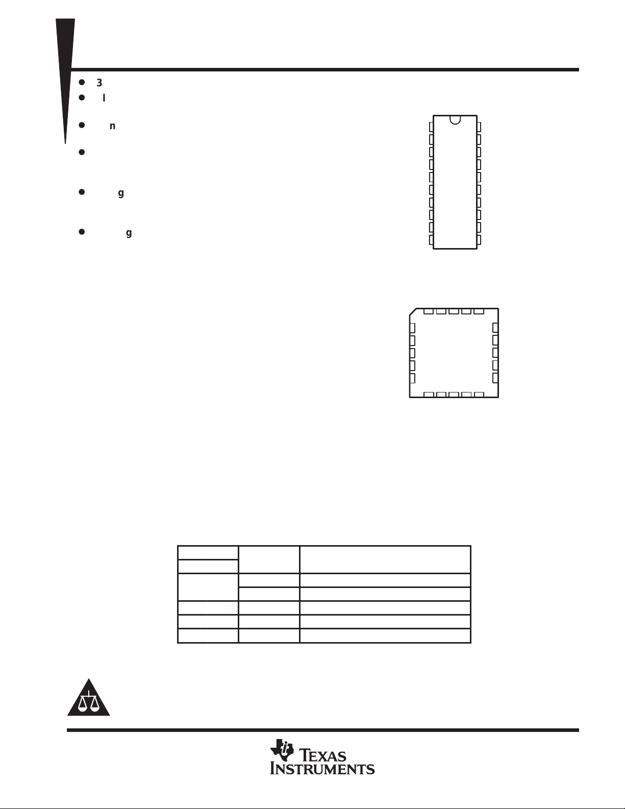
SN54ACT1284 ...J OR W PACKAGE
SN74ACT1284 . . . DB, DW, N, OR PW PACKAGE
A4
GND
GND
A5
A6
(TOP VIEW)
A1
1
A2
2
A3
3
A4
4
GND
GND
A5
A6
A7
DIR
FK PACKAGE
(TOP VIEW)
5
6
7
8
9
10
A3A2A1
3212019
4
5
6
7
8
9
10 11 12 13
A7
DIR
HD
20
19
18
17
16
15
14
13
12
11
B1
B7
B2
18
17
16
15
14
B6
B1
B2
B3
B4
V
V
B5
B6
B7
HD
CC
CC
B3
B4
V
V
B5
CC
CC
The output drive for each mode is determined by the high drive (HD) control pin. When HD is high, the high drive
is delivered by the totem-pole configuration, and when HD is low, the outputs are open drain. This meets the
drive requirements as specified in the IEEE 1284-I (level 1 type) and the IEEE 1284-II (level 2 type) parallel
peripheral-interface specification.
The SN54ACT1284 is characterized for operation over the full military temperature range of –55°C to 125°C.
The SN74ACT1284 is characterized for operation from 0°C to 70°C.
FUNCTION TABLE
INPUTS
DIR HD
Open drain A to B: Bits 5, 6, 7
Totem pole B to A: Bits 1, 2, 3, 4
L H Totem pole B to A: Bits 1, 2, 3, 4 and A to B: Bits 5, 6, 7
H L Open drain A to B: Bits 1, 2, 3, 4, 5, 6, 7
H H Totem pole A to B: Bits 1, 2, 3, 4, 5, 6, 7
Please be aware that an important notice concerning availability, standard warranty, and use in critical applications of
Texas Instruments semiconductor products and disclaimers thereto appears at the end of this data sheet.
UNLESS OTHERWISE NOTED this document contains PRODUCTION
DATA information current as of publication date. Products conform to
specifications per the terms of Texas Instruments standard warranty.
Production processing does not necessarily include testing of all
parameters.
Copyright 1996, Texas Instruments Incorporated
POST OFFICE BOX 655303 • DALLAS, TEXAS 75265
1
SN54ACT1284, SN74ACT1284
7-BIT BUS INTERFACES
WITH 3-STATE OUTPUTS
SCAS459B – NOVEMBER 1994 – REVISED APRIL 1996
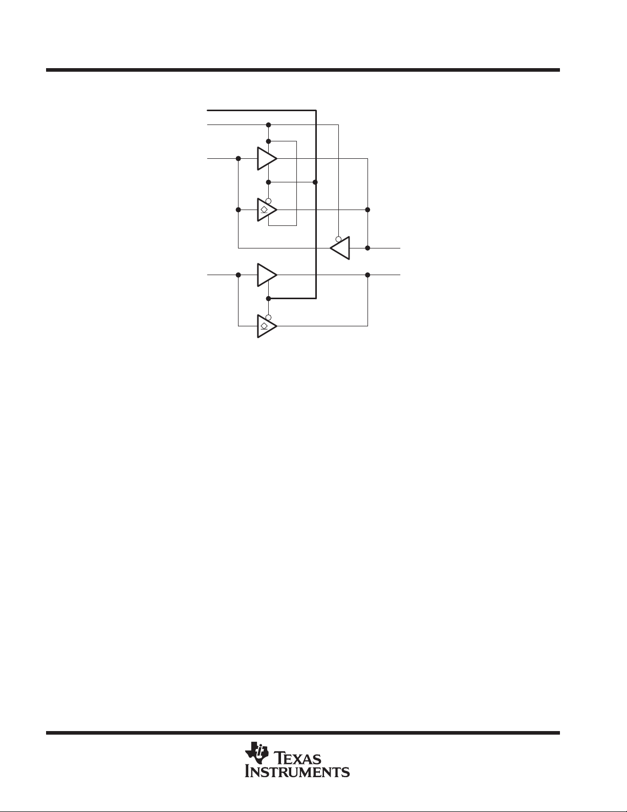
logic diagram (positive logic)
HD
DIR
A1, A2, A3, A4
B1, B2, B3, B4
A5, A6, A7
B5, B6, B7
absolute maximum ratings over operating free-air temperature range (unless otherwise noted)
Supply voltage range, VCC –0.5 V to 7 V. . . . . . . . . . . . . . . . . . . . . . . . . . . . . . . . . . . . . . . . . . . . . . . . . . . . . . . . . .
B-port input and output voltage range, VI and VO (see Notes 1 and 2) –2 V to 7 V. . . . . . . . . . . . . . . . . . . . . .
A-port input and output voltage range, V
Input clamp current, IIK (VI < 0 or VI > VCC) ±20 mA. . . . . . . . . . . . . . . . . . . . . . . . . . . . . . . . . . . . . . . . . . . . . . . .
Output clamp current, IOK (VO < 0 or VO > VCC) ±50 mA. . . . . . . . . . . . . . . . . . . . . . . . . . . . . . . . . . . . . . . . . . . .
Continuous output current, IO (VO = 0 to VCC) ±50 mA. . . . . . . . . . . . . . . . . . . . . . . . . . . . . . . . . . . . . . . . . . . . . .
Continuous current through V
Package thermal impedance, θ
Storage temperature range, T
†
Stresses beyond those listed under “absolute maximum ratings” may cause permanent damage to the device. These are stress ratings only, and
functional operation of the device at these or any other conditions beyond those indicated under “recommended operating conditions” is not
implied. Exposure to absolute-maximum-rated conditions for extended periods may affect device reliability.
NOTES: 1. The input and output voltage ratings may be exceeded if the input and output current ratings are observed.
2. The ac input voltage pulsewidth is limited to 20 ns if the input voltage goes more negative than –0.5 V.
3. The package thermal impedance is calculated in accordance with JESD 51, except for through-hole packages, which use a trace
length of zero.
or GND ±200 mA. . . . . . . . . . . . . . . . . . . . . . . . . . . . . . . . . . . . . . . . . . . . . . . . .
CC
JA
–65°C to 150°C. . . . . . . . . . . . . . . . . . . . . . . . . . . . . . . . . . . . . . . . . . . . . . . . . .
stg
and VO (see Note 1) –0.5 V to VCC + 0.5 V. . . . . . . . . . . . . . . . . . . .
I
(see Note 3): DB package 115°C/W. . . . . . . . . . . . . . . . . . . . . . . . . . . . . . . .
DW package 97°C/W. . . . . . . . . . . . . . . . . . . . . . . . . . . . . . . . .
N package 67°C/W. . . . . . . . . . . . . . . . . . . . . . . . . . . . . . . . . . .
PW package 128°C/W. . . . . . . . . . . . . . . . . . . . . . . . . . . . . . . .
†
2
POST OFFICE BOX 655303 • DALLAS, TEXAS 75265

UNIT
IOHHigh-level output current
mA
IOLLow-level output current
mA
PARAMETER
TEST CONDITIONS
V
†
UNIT
V
V
V
for all inputs
V
A port
4.7 V
PARAMETER
UNIT
Totem pole
A or B
B or A
ns
Totem poleHDB
ns
SN54ACT1284, SN74ACT1284
7-BIT BUS INTERFACES
WITH 3-STATE OUTPUTS
SCAS459B – NOVEMBER 1994 – REVISED APRIL 1996
recommended operating conditions
SN54ACT1284 SN74ACT1284
MIN MAX MIN MAX
V
V
V
V
V
T
electrical characteristics over recommended ranges of operating free-air temperature and supply
voltage (unless otherwise noted)
V
V
I
I
I
OZ
I
OFF
I
CC
C
C
Z
†
For I/O ports, the parameter IOZ includes the input leakage current II.
‡
For conditions shown as MIN or MAX, use the appropriate values under recommended operating conditions.
Supply voltage 4.7 5.5 4.7 5.5 V
CC
High-level input voltage 2 2 V
IH
Low-level input voltage 0.8 0.8 V
IL
Input voltage 0 V
I
Open drain output voltage HD low 0 5.5 0 5.5 V
O
p
p
Operating free-air temperature –55 125 0 70 °C
A
CC
Input
hys
hysteresis
B port IOH = –14 mA 4.7 V 2.4 2.4
OH
A port
B port IOL =14 mA 4.7 V 0.4 0.4
OL
p
A or B ports‡VO = VCC or GND 5.5 V ±20 ±20 µA
B port VI or VO ≤ 7 V 0 V ±100 ±100 µA
Control inputs VI = VCC or GND 5 V 4 4 pF
i
A or B ports VO = VCC or GND 5 V 12 12 pF
io
B port IOH = –20 mA, IOH = –50 mA 5 V 8 30 8 30 Ω
O
–
IT–
IT+
IOH = –50 µA
IOH = –4 mA 4.7 V 3.7 3.7
IOL = 50 µA
IOL = 4 mA
VI = VCC or GND 5.5 V ±1 ±1 µA
VI = VCC or GND, IO = 0 5.5 V 1.5 1.5 mA
p
5 V 0.4 0.4
4.7 V 0.2 0.2
MIN
to MAX
B port, HD high –14 –14
A port –4 –4
B port 14 14
A port 4 4
SN54ACT1284 SN74ACT1284
MIN TYP MAX MIN TYP MAX
VCC–0.2 VCC–0.2
0.2 0.2
0.4 0.4
CC
0 V
CC
V
V
V
switching characteristics over recommended ranges of supply voltage and operating free-air
temperature (unless otherwise noted) (see Figure 1)
t
PLH
t
PHL
SR Totem pole B output 0.05 0.4 0.05 0.4 V/ns
tpd(EN)
tpd(DIS)
tr, t
PRODUCT PREVIEW information concerns products in the formative or
design phase of development. Characteristic data and other
specifications are design goals. Texas Instruments reserves the right to
change or discontinue these products without notice.
FROM TO
(INPUT) (OUTPUT)
p
p
f
Open drain A B 120 120 ns
POST OFFICE BOX 655303 • DALLAS, TEXAS 75265
SN54ACT1284 SN74ACT1284
MIN MAX MIN MAX
1 20 1 20
1 20 1 20
1 20 1 20
1 20 1 20
3

SN54ACT1284, SN74ACT1284
7-BIT BUS INTERFACES
WITH 3-STATE OUTPUTS
SCAS459B – NOVEMBER 1994 – REVISED APRIL 1996
PARAMETER MEASUREMENT INFORMATION
V
CC
From B Output
Under Test
TP1
33 Ω
From B Output
62 Ω
t
PHL
t
PLH
A-TO-B LOAD (totem pole)
CL = 50 pF
(see Note A)
Sink Load
Source Load
62 Ω
V
TP1
CL = 50 pF
(see Note A)
CL = 50 pF
(see Note A)
CC
500 Ω
Input
(see Note C)
Output
(see Note D)
V
OH
V
OL
Input
(see Note F)
V
(see Note E)
OL
1.5 V1.5 V
t
PLH
VOLTAGE WAVEFORMS MEASURED AT TP1
PROPAGATION DELAY TIMES (A to B)
1.5 V
0.8 V
t
r
VOLTAGE WAVEFORMS MEASURED AT TP1 (B SIDE)
1.5 V
t
PHL
1.5 V
VOH – 1.4 VVOH – 1.4 VVOL + 1.4 V
2 V2 V
0.8 V
t
f
3 V
0 V
V
VOLV
3 V
0 V
V
V
OH
OL
OH
OL
A-TO-B LOAD (open drain)
From A Output
Under Test
CL = 50 pF
(see Note A)
B-TO-A LOAD (totem pole)
NOTES: A. CL includes probe and jig capacitance.
B. The outputs are measured one at a time with one transition per measurement.
C. Input rise and fall times are 3 ns, 150 ns < pulsewidth <10 µs for both low-to-high and high-to-low transitions.
D. Slew rate is defined as 10% and 90% of the transition times.
E. Rise and fall times, open drain, are <120 ns.
F. Input rise and fall times are 3 ns.
500 Ω
Figure 1. Load Circuits and Voltage Waveforms
4
POST OFFICE BOX 655303 • DALLAS, TEXAS 75265
Input
(see Note F)
Output
CC
1.5 V
t
PHL
1.5 V1.5 V
t
PLH
50% V
VOLTAGE WAVEFORMS
PROPAGATION DELAY TIMES (B to A)
50% V
CC
3 V
0 V
V
VOLV
OH
OL

IMPORTANT NOTICE
T exas Instruments and its subsidiaries (TI) reserve the right to make changes to their products or to discontinue
any product or service without notice, and advise customers to obtain the latest version of relevant information
to verify, before placing orders, that information being relied on is current and complete. All products are sold
subject to the terms and conditions of sale supplied at the time of order acknowledgement, including those
pertaining to warranty, patent infringement, and limitation of liability.
TI warrants performance of its semiconductor products to the specifications applicable at the time of sale in
accordance with TI’s standard warranty. Testing and other quality control techniques are utilized to the extent
TI deems necessary to support this warranty . Specific testing of all parameters of each device is not necessarily
performed, except those mandated by government requirements.
CERTAIN APPLICA TIONS USING SEMICONDUCT OR PRODUCTS MAY INVOLVE POTENTIAL RISKS OF
DEATH, PERSONAL INJURY, OR SEVERE PROPERTY OR ENVIRONMENTAL DAMAGE (“CRITICAL
APPLICATIONS”). TI SEMICONDUCTOR PRODUCTS ARE NOT DESIGNED, AUTHORIZED, OR
WARRANTED TO BE SUITABLE FOR USE IN LIFE-SUPPORT DEVICES OR SYSTEMS OR OTHER
CRITICAL APPLICA TIONS. INCLUSION OF TI PRODUCTS IN SUCH APPLICATIONS IS UNDERST OOD TO
BE FULLY AT THE CUSTOMER’S RISK.
In order to minimize risks associated with the customer’s applications, adequate design and operating
safeguards must be provided by the customer to minimize inherent or procedural hazards.
TI assumes no liability for applications assistance or customer product design. TI does not warrant or represent
that any license, either express or implied, is granted under any patent right, copyright, mask work right, or other
intellectual property right of TI covering or relating to any combination, machine, or process in which such
semiconductor products or services might be or are used. TI’s publication of information regarding any third
party’s products or services does not constitute TI’s approval, warranty or endorsement thereof.
Copyright 1998, Texas Instruments Incorporated
 Loading...