


www.DataSheet4U.com
www.ti.com
MULTIPOINT-LVDS LINE DRIVER AND RECEIVER
FEATURES DESCRIPTION
• Low-Voltage Differential 30- Ω to 55- Ω Line
Drivers and Receivers for Signaling Rates
Up to 100 Mbps, Clock Frequencies up to
50 MHz
• Type-1 Receivers Incorporate 25 mV of
Hysteresis (200A, 202A)
• Type-2 Receivers Provide an Offset(100 mV)
Threshold to Detect Open-Circuit and Idle-Bus
Conditions (204A, 205A)
• Meets or Exceeds the M-LVDS Standard
TIA/EIA-899 for Multipoint Data Interchange
• Power Up/Down Glitch Free
• Controlled Driver Output Voltage Transition
Times for Improved Signal Quality
• –1 V to 3.4 V Common-Mode Voltage Range
Allows Data Transfer With 2 V of Ground
Noise
• Bus Pins High Impedance When Disabled or
V
≤ 1.5 V
CC
• 200-Mbps Devices Available (SN65MLVD201,
203, 206, 207)
• Bus Pin ESD Protection Exceeds 8 kV
• Package in 8-Pin SOIC (200A, 204A) and
14-Pin SOIC (202A, 205A)
• Improved Alternatives to the SN65MLVD200,
202, 204, and 205
APPLICATIONS
• Low-Power High-Speed Short-Reach
Alternative to TIA/EIA-485
• Backplane or Cabled Multipoint Data and
Clock Transmission
• Cellular Base Stations
• Central-Office Switches
• Network Switches and Routers
(1) The signaling rate of a line, is the number of voltage
transitions that are made per second expressed in the nits
bps (bits per second).
SN65MLVD200A , SN65MLVD202A
SN65MLVD204A , SN65MLVD205A
SLLS573 – DECEMBER 2003
(1)
The SN65MLVD200A, 202A, 204A, and 205A are
multipoint-low-voltage differential (M-LVDS) line
drivers and receivers, which are optimized to operate
at signaling rates up to 100 Mbps. All parts comply
with the multipoint low-voltage differential signaling
(M-LVDS) standard TIA/EIA-899. These circuits are
similar to their TIA/EIA-644 standard compliant LVDS
counterparts, with added features to address
multipoint applications. The driver output has been
designed to support multipoint buses presenting
loads as low as 30 Ω , and incorporates controlled
transition times to allow for stubs off of the backbone
transmission line.
These devices have Type-1 and Type-2 receivers
that detect the bus state with as little as 50 mV of
differential input voltage over a common-mode
voltage range of –1 V to 3.4 V. The Type-1 receivers
exhibit 25 mV of differential input voltage hysteresis
to prevent output oscillations with slowly changing
signals or loss of input. Type-2 receivers include an
offset threshold to provide a known output state
under open-circuit, idle-bus, and other fault
conditions.
The SN65MLVD200A, 202A, 204A, and 205A have
enhancements over their predecessors. Improved
features include better controlled slew rate on the
driver output to help minimize reflections while
improving overall signal integrity (SI) resulting in
better jitter performance. Additionally, 8-kV ESD
protection on the bus pins for more robustness. The
same footprint definition was maintained making for
an easy drop-in replacement for a system
performance upgrade.
The devices are characterized for operation from
–40 ° C to 85 ° C.
Please be aware that an important notice concerning availability, standard warranty, and use in critical applications of Texas
Instruments semiconductor products and disclaimers thereto appears at the end of this data sheet.
PRODUCTION DATA information is current as of publication date.
Products conform to specifications per the terms of the Texas
Instruments standard warranty. Production processing does not
necessarily include testing of all parameters.
Copyright © 2003–TBD, Texas Instruments Incorporated
www.ti.com
4
3
1
2
DE
D
RE
R
6
7
A
B
LOGIC DIAGRAM (POSITIVE LOGIC)
5
4
2
3
DE
D
RE
R
12
11
A
B
10
9
Y
Z
SN65MLVD202A, SN65MLVD205A
SN65MLVD200A, SN65MLVD204A
SN65MLVD200A , SN65MLVD202A
SN65MLVD204A , SN65MLVD205A
SLLS573 – DECEMBER 2003
These devices have limited built-in ESD protection. The leads should be shorted together or the device placed in conductive foam
during storage or handling to prevent electrostatic damage to the MOS gates.
ORDERING INFORMATION
PART NUMBER
SN65MLVD200AD SN75176 Type 1 MF200A
SM65MLVD202AD SN75ALS180 Type 1 MLVD202A
SN65MLVD204AD SN75176 Type 2 MF204A
SM65MLVD205AD SN75ALS180 Type 2 MLVD205A
(1) Available tape and reeled. To order a tape and reeled part, add the suffix R to the part number (e.g., SN65MLVD200ADR).
(1)
FOOTPRINT RECEIVER TYPE PACKAGE MARKING
PACKAGE DISSIPATION RATINGS
PACKAGE
D(8) 532 mW 4.6 mW/ ° C 254 mW
D(14) 940 mW 8.2 mW/ ° C 450 mw
POWER RATING ABOVE TA= 25°C POWER RATING
ABSOLUTE MAXIMUM RATINGS
over operating free-air temperature range unless otherwise noted
Supply voltage range
Input voltage range A, B (200A, 204A) –1.8 V to 4 V
Output voltage range
Electrostatic discharge All pins ± 4 kV
Continuous power dissipation See Dissipation Rating Table
Storage temperature range –65 ° C to 150 ° C
(1) Stresses beyond those listed under absolute maximum ratings may cause permanent damage to the device. These are stress ratings
only, and functional operation of the device at these or any other conditions beyond those indicated under recommended operating
conditions is not implied. Exposure to absolute-maximum-rated conditions for extended periods may affect device reliability.
(2) All voltage values, except differential I/O bus voltages, are with respect to network ground terminal.
(3) Tested in accordance with JEDEC Standard 22, Test Method A114-A.
(4) Tested in accordance with JEDEC Standard 22, Test Method C101.
2
(2)
, V
CC
D, DE, RE –0.5 V to 4 V
A, B (202A, 205A) –4 V to 6 V
R –0.3 V to 4 V
Y, Z, A, or B –1.8 V to 4 V
Human Body Model
Charged-Device Model
TA≤ 25 ° C DERATING FACTOR TA= 85 ° C
(1)
SN65MLVD200A,
202A, 204A, and 205A
–0.5 V to 4 V
(3)
A, B, Y, and Z ± 8 kV
(4)
All pins ± 1500 V
Submit Documentation Feedback
www.ti.com
SN65MLVD200A , SN65MLVD202A
SN65MLVD204A , SN65MLVD205A
RECOMMENDED OPERATING CONDITIONS
MIN NOM MAX UNIT
V
V
V
|V
R
1/t
T
DEVICE ELECTRICAL CHARACTERISTICS
over recommended operating conditions unless otherwise noted
I
P
(1) All typical values are at 25 ° C and with a 3.3-V supply voltage.
Supply voltage 3 3.3 3.6 V
CC
High-level input voltage 2 V
IH
Low-level input voltage GND 0.8 V
IL
Voltage at any bus terminal VA, VB,VYor V
| Magnitude of differential input voltage 0.05 V
ID
Differential load resistance 30 50 Ω
L
Signaling rate 100 Mbps
UI
Operating free-air temperature –40 85 ° C
A
Z
–1.4 3.8 V
PARAMETER TEST CONDITIONS MIN MAX UNIT
Driver only RE and DE at VCC, RL= 50 Ω , All others open 13 22
Supply current mA
CC
Both disabled RE at VCC, DE at 0 V, RL= No Load, All others open 1 4
Both enabled RE at 0 V, DE at VCC, RL= 50 Ω , All others open 16 24
Receiver only RE at 0 V, DE at 0 V, All others open 4 13
Device power dissipation 94 mW
D
RL= 50 Ω , Input to D is a 50-MHz 50% duty cycle square
wave, DE = high, RE = low, TA= 85 ° C
SLLS573 – DECEMBER 2003
CC
CC
(
(1)
TYP
)
V
V
Submit Documentation Feedback
3
www.ti.com
SN65MLVD200A , SN65MLVD202A
SN65MLVD204A , SN65MLVD205A
SLLS573 – DECEMBER 2003
DRIVER ELECTRICAL CHARACTERISTICS
over recommended operating conditions unless otherwise noted
(1)
–50 50 mV
SS
|V
| or
AB
|V
YZ
∆ |V
∆ |V
V
OS(SS)
∆ V
OS(SS)
V
OS(PP)
V
Y(OC)
V
A(OC)
V
Z(OC)
V
B(OC)
V
P(H)
V
P(L)
I
IH
I
IL
Differential output voltage magnitude 480 650 mV
|
| or Change in differential output voltage magnitude
AB
| between logic states
YZ
Steady-state common-mode output voltage 0.8 1.2 V
Change in steady-state common-mode output
voltage between logic states
Peak-to-peak common-mode output voltage 150 mV
or
Maximum steady-state open-circuit output voltage 0 2.4 V
or
Maximum steady-state open-circuit output voltage 0 2.4 V
Voltage overshoot, low-to-high level output 1.2 V
Voltage overshoot, high-to-low level output –0.2 V
High-level input current (D, DE) VIH= 2 V to V
Low-level input current (D, DE) VIL= GND to 0.8 V 0 10 µA
PARAMETER TEST CONDITIONS MIN
See Figure 2
See Figure 3 –50 50 mV
See Figure 7
See Figure 5
CC
|IOS| Differential short-circuit output current magnitude See Figure 4 24 mA
I
OZ
I
O(OFF)
CYor C
C
YZ
C
Y/Z
High-impedance state output current (driver only) –15 10 µA
Power-off output current –10 10 µA
–1.4 V ≤ (V
Other output = 1.2 V
–1.4 V ≤ (V
output = 1.2 V, 0 V ≤ VCC≤ 1.5 V
VI= 0.4 sin(30E6 π t) + 0.5 V,
Output capacitance Other input at 1.2 V, driver 3 pF
Z
Differential output capacitance 2.5 pF
Output capacitance balance, (C
) 0.99 1.01
Y/CZ
disabled
V
= 0.4 sin(30E6 π t) V,
AB
Driver disabled
or VZ) ≤ 3.8 V,
Y
or VZ) ≤ 3.8 V, Other
Y
(3)
(3)
(1) The algebraic convention, in which the least positive (most negative) limit is designated as minimum is used in this data sheet.
(2) All typical values are at 25 ° C and with a 3.3-V supply voltage.
(3) HP4194A impedance analyzer (or equivalent)
(2)
TYP
MAX UNIT
0 10 µA
V
SS
V
4
Submit Documentation Feedback
www.ti.com
SN65MLVD200A , SN65MLVD202A
SN65MLVD204A , SN65MLVD205A
RECEIVER ELECTRICAL CHARACTERISTICS
over recommended operating conditions unless otherwise noted
PARAMETER TEST CONDITIONS MIN TYP
V
IT+
V
IT-
V
HYS
V
OH
V
OL
I
IH
I
IL
I
OZ
CAor VI= 0.4 sin(30E6 π t) + 0.5 V,
C
B
C
AB
C
A/B
Positive-going differential input voltage threshold mV
Negative-going differential input voltage threshold mV
Differential input voltage hysteresis, (V
– V
IT+
High-level output voltage IOH= –8 mA 2.4 V
Low-level output voltage IOL= 8 mA 0.4 V
High-level input current ( RE) VIH= 2 V to V
Low-level input current ( RE) VIL= GND to 0.8 V –10 0 µA
High-impedance output current VO= 0 V or 3.6 V –10 15 µA
Input capacitance 3 pF
Differential input capacitance V
Input capacitance balance, (C
) 0.99 1.01
A/CB
(1) All typical values are at 25 ° C and with a 3.3-V supply voltage.
(2) HP4194A impedance analyzer (or equivalent)
Type 1 50
Type 2 150
Type 1 –50
Type 2 50
Type 1 25
) mV
IT–
Type 2 0
See Figure 9, Table 1 and Table
2
CC
Other input at 1.2 V
= 0.4 sin(30E6 π t) V
AB
SLLS573 – DECEMBER 2003
(1)
MAX UNIT
–10 0 µA
(2)
(2)
2.5 pF
BUS INPUT AND OUTPUT ELECTRICAL CHARACTERISTICS
over recommended operating conditions unless otherwise noted
PARAMETER TEST CONDITIONS MIN TYP
I
I
I
I
I
I
C
C
C
C
Receiver or transceiver with driver disabled
A
input current
Receiver or transceiver with driver disabled
B
input current
Receiver or transceiver with driver disabled
AB
differential input current (IA– IB)
Receiver or transceiver power-off input current VA= 0 V or 2.4 V, VB= 1.2 V, 0 V ≤ VCC≤ 1.5 V –20 20 µA
A(OFF)
Receiver or transceiver power-off input current VB= 0 V or 2.4 V, VA= 1.2 V, 0 V ≤ VCC≤ 1.5 V –20 20 µA
B(OFF)
Receiver input or transceiver power-off
AB(OFF)
differential input current (IA– IB)
Transceiver with driver disabled input
A
capacitance
Transceiver with driver disabled input
B
capacitance
Transceiver with driver disabled differential
AB
input capacitance
Transceiver with driver disabled input
A/B
capacitance balance, (CA/CB)
(1) All typical values are at 25 ° C and with a 3.3-V supply voltage.
(2) HP4194A impedance analyzer (or equivalent)
VA= 3.8 V, VB= 1.2 V, 0 32
VA= 0 V or 2.4 V, VB= 1.2 V –20 20 µA
VA= -1.4 V, VB= 1.2 V –32 0
VB= 3.8 V, VA= 1.2 V 0 32
VB= 0 V or 2.4 V, VA= 1.2 V –20 20 µA
VB= -1.4 V, VA= 1.2 V –32 0
VA= V
VA= 3.8 V, VB= 1.2 V, 0 V ≤ VCC≤ 1.5 V 0 32
VA= -1.4 V, VB= 1.2 V, 0 V ≤ VCC≤ 1.5 V –32 0
VB= 3.8 V, VA= 1.2 V, 0 V ≤ VCC≤ 1.5 V 0 32
VB= -1.4 V, VA= 1.2 V, 0 V ≤ VCC≤ 1.5 V –32 0
VA= VB, 0 V ≤ VCC≤ 1.5 V, –1.4 ≤ VA≤ 3.8 V –4 4 µA
VA= 0.4 sin (30E6 π t) + 0.5 V
VB= 0.4 sin (30E6 π t) + 0.5 V
VAB= 0.4 sin (30E6 π t)V
(1)
MAX UNIT
B,
1.4 ≤ VA≤ 3.8 V -4 4 µA
(2)
, VB=1.2 V 5 pF
(2)
, VA=1.2 V 5 pF
(2)
0.99 1.01
3 pF
Submit Documentation Feedback
5
www.ti.com
SN65MLVD200A , SN65MLVD202A
SN65MLVD204A , SN65MLVD205A
SLLS573 – DECEMBER 2003
DRIVER SWITCHING CHARACTERISTICS
over recommended operating conditions unless otherwise noted
PARAMETER TEST CONDITIONS MIN TYP
t
t
t
t
t
t
t
t
t
t
t
t
(1) All typical values are at 25 ° C and with a 3.3-V supply voltage.
(2) Jitter is ensured by design and characterization. Stimulus jitter has been subtracted from the numbers.
(3) tr= tf= 0.5 ns (10% to 90%), measured over 30 k samples.
(4) Peak-to-peak jitter includes jitter due to pulse skew (t
(5) tr= tf= 0.5 ns (10% to 90%), measured over 100 k samples.
Propagation delay time, low-to-high-level output 2 2.5 3.5 ns
pLH
Propagation delay time, high-to-low-level output 2 2.5 3.5 ns
pHL
Differential output signal rise time 2 2.6 3.2 ns
r
Differential output signal fall time 2 2.6 3.2 ns
f
Pulse skew (|t
sk(p)
Part-to-part skew 0.9 ns
sk(pp)
Period jitter, rms (1 standard deviation)
jit(per)
Peak-to-peak jitter
jit(pp)
Disable time, high-level-to-high-impedance output 4 7 ns
PHZ
Disable time, low-level-to-high-impedance output 4 7 ns
PLZ
Enable time, high-impedance-to-high-level output 4 7 ns
PZH
Enable time, high-impedance-to-low-level output 4 7 ns
PZL
– t
pHL
|) 30 150 ps
pLH
(2)
(2) (4)
).
sk(p)
See Figure 5
50 MHz clock input
100 Mbps 215-1 PRBS input
See Figure 6
(1)
MAX UNIT
(3)
(5)
2 3 ps
55 150 ps
RECEIVER SWITCHING CHARACTERISTICS
over recommended operating conditions unless otherwise noted
PARAMETER TEST CONDITIONS MIN MAX UNIT
t
t
t
t
t
t
t
t
t
t
t
t
(1) All typical values are at 25 ° C and with a 3.3-V supply voltage.
(2) HP4194A impedance analyzer (or equivalent)
(3) Jitter is ensured by design and characterization. Stimulus jitter has been subtracted from the numbers.
(4) VID= 200 mV
(5) Peak-to-peak jitter includes jitter due to pulse skew (t
(6) VID= 200 mV
Propagation delay time, low-to-high-level output 2 3.6 6 ns
PLH
Propagation delay time, high-to-low-level output 2 3.6 6 ns
PHL
Output signal rise time 1 2.3 ns
r
Output signal fall time CL= 15 pF, See Figure 10 1 2.3 ns
f
Pulse skew (|t
sk(p)
Part-to-part skew
sk(pp)
Period jitter, rms (1 standard deviation)
jit(per)
Peak-to-peak jitter
jit(pp)
Disable time, high-level-to-high-impedance output 6 10 ns
PHZ
Disable time, low-level-to-high-impedance output 6 10 ns
PLZ
Enable time, high-impedance-to-high-level output 10 15 ns
PZH
Enable time, high-impedance-to-low-level output 10 15 ns
PZL
samples.
samples.
– t
pHL
(LVD200A, 202A), VID= 400 mV
pp
(LVD200A, 202A), VID= 400 mV
pp
|)
pLH
(2)
(3) (5)
(3)
pp
(LVD204A, 205A), V
pp
(LVD204A, 205A), V
Type 1 100 300 ps
Type 2 300 500 ps
50 MHz clock input
Type 1 200 700 ps
Type 2 225 800 ps
100 Mbps 215–1 PRBS input
See Figure 11
= 1 V, tr= tf= 0.5 ns (10% to 90%), measured over 30 k
cm
).
sk(p)
= 1 V, tr= tf= 0.5 ns (10% to 90%), measured over 100 k
cm
(1)
TYP
(1)
1 ns
(4)
(6)
4 7 ps
6
Submit Documentation Feedback
www.ti.com
VAB or V
YZ
A/Y
B/Z
I
A
or I
Y
VB or V
Z
VA or V
Y
V
OS
VA + V
B
2
V
I
D
V
CC
VY + V
Z
2
or
I
B
or I
Z
I
I
VAB or V
YZ
49.9 Ω
3.32 kΩ
3.32 kΩ
_
+
-1 V ≤ V
test
≤ 3.4 V
A/Y
B/Z
D
V
OS
R1
24.9 Ω
A/Y
C3
2.5 pF
V
OS(PP)
V
OS(SS)
V
OS(SS)
≈ 1.3 V
B/Z
A/Y
≈ 0.7 V
B/Z
D
R2
24.9 Ω
C1
1 pF
C2
1 pF
V
Test
+
-
A/Y
B/Z
I
OS
0 V or V
CC
-1 V or 3.4 V
A. All resistors are 1% tolerance.
SN65MLVD200A , SN65MLVD202A
SN65MLVD204A , SN65MLVD205A
SLLS573 – DECEMBER 2003
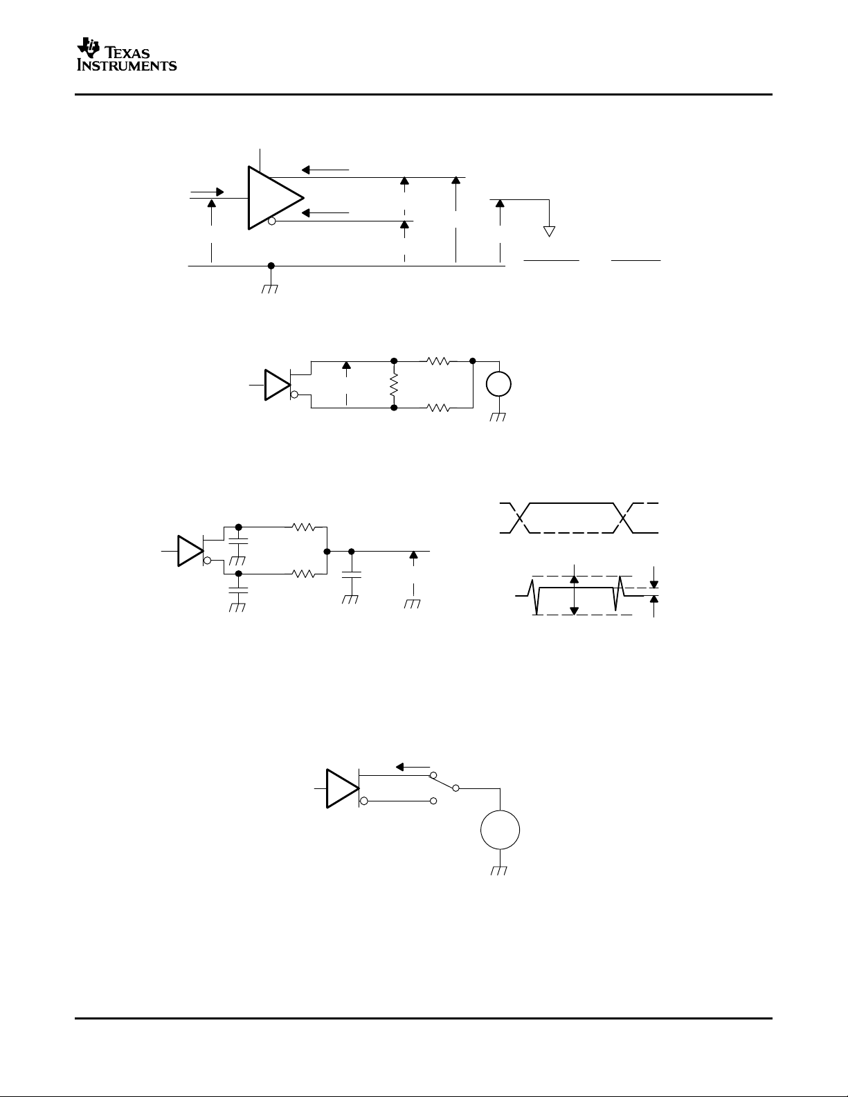
PARAMETER MEASUREMENT INFORMATION
Figure 1. Driver Voltage and Current Definitions
Figure 2. Differential Output Voltage Test Circuit
A. All input pulses are supplied by a generator having the following characteristics: tror tf≤ 1 ns, pulse frequency = 1
MHz, duty cycle = 50 ± 5%.
B. C1, C2 and C3 include instrumentation and fixture capacitance within 2 cm of the D.U.T. and are ±20%.
C. R1 and R2 are metal film, surface mount, ±1%, and located within 2 cm of the D.U.T.
D. The measurement of V
is made on test equipment with a -3 dB bandwidth of at least 1 GHz.
OS(PP)
Figure 3. Test Circuit and Definitions for the Driver Common-Mode Output Voltage
Figure 4. Driver Short-Circuit Test Circuit
Submit Documentation Feedback
7
www.ti.com
Output
A/Y
Output
t
pLH
t
pHL
Input
C3
0.5 pF
B/Z
D
0 V
0.9V
V
0 V
t
f
t
r
V
CC
VCC/2
0 V
SS
SS
0 V
0.1V
SS
SS
C1
1 pF
C2
1 pF
V
P(H)
V
P(L)
R1
50 Ω
A/Y
B/Z
R1
24.9 Ω
t
pZH
t
pHZ
t
pZL
t
pLZ
V
CC
VCC/2
0 V
∼ 0.6 V
0.1 V
0 V
∼ -0.6 V
0 V
-0.1 V
DE
Output With
D at V
CC
Output
0 V or V
CC
DE
Output With
D at 0 V
C1
1 pF
R2
24.9 Ω
C4
0.5 pF
C2
1 pF
D
C3
2.5 pF
SN65MLVD200A , SN65MLVD202A
SN65MLVD204A , SN65MLVD205A
SLLS573 – DECEMBER 2003
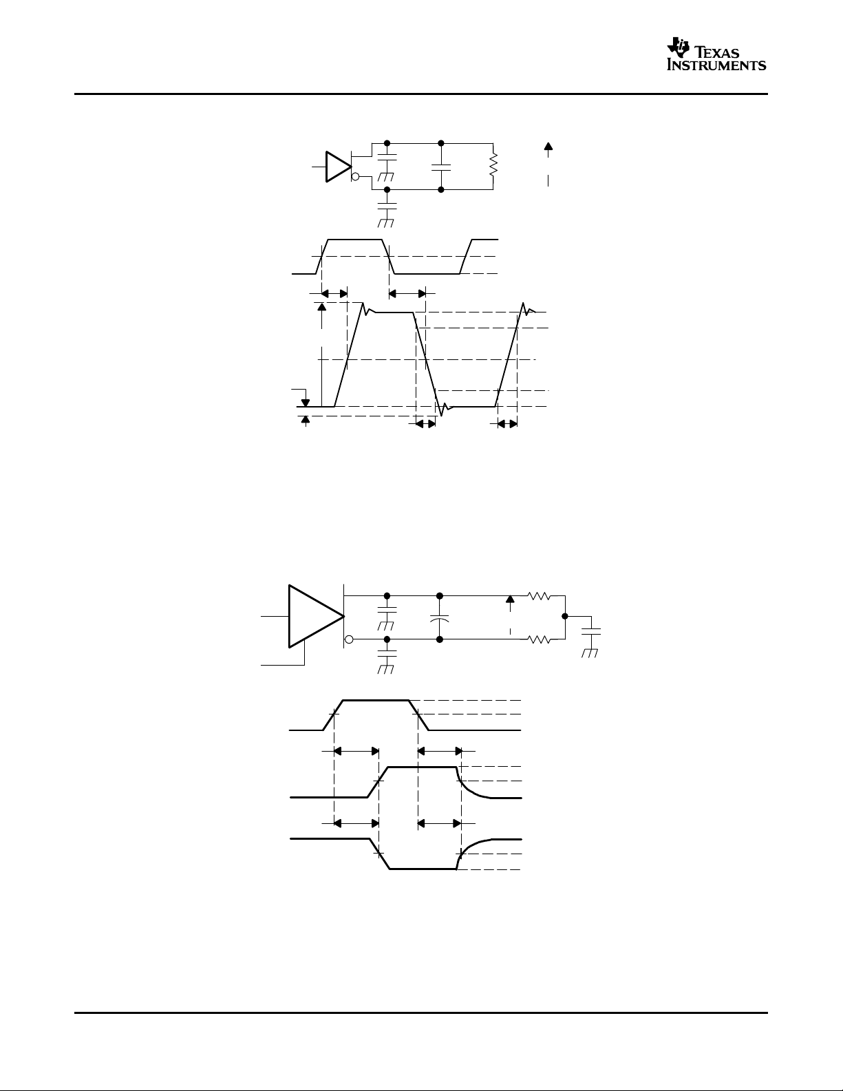
PARAMETER MEASUREMENT INFORMATION (continued)
A. All input pulses are supplied by a generator having the following characteristics: tror tf≤ 1 ns, frequency = 1 MHz,
duty cycle = 50 ± 5%.
B. C1, C2, and C3 include instrumentation and fixture capacitance within 2 cm of the D.U.T. and are ±20%.
C. R1 is a metal film, surface mount, and 1% tolerance and located within 2 cm of the D.U.T.
D. The measurement is made on test equipment with a -3 dB bandwidth of at least 1 GHz.
Figure 5. Driver Test Circuit, Timing, and Voltage Definitions for the Differential Output Signal
A. All input pulses are supplied by a generator having the following characteristics: tror tf≤ 1 ns, frequency = 1 MHz,
B. C1, C2, C3, and C4 includes instrumentation and fixture capacitance within 2 cm of the D.U.T. and are ±20%.
C. R1 and R2 are metal film, surface mount, and 1% tolerance and located within 2 cm of the D.U.T.
D. The measurement is made on test equipment with a -3 dB bandwidth of at least 1 GHz.
duty cycle = 50 ± 5%.
Figure 6. Driver Enable and Disable Time Circuit and Definitions
8
Submit Documentation Feedback

www.ti.com
A/Y
B/Z
0 V or V
CC
1.62 kΩ , ±1%
VA, VB, VY or V
Z
t
c(n)
1/f0
0 V
0 V
Period Jitter
0 V Diff
Peak to Peak Jitter
1/f0
PRBS INPUT
OUTPUT
VA -VB or VY -V
Z
VA -VB or VY -V
Z
CLOCK
INPUT
IDEAL
OUTPUT
ACTUAL
OUTPUT
V
CC
VCC/2
t
jit(per)
= t
c(n)
-1/f0
t
jit(pp)
0 V
V
CC
VCC/2
0 V
VA -VB or VY -V
Z
VA -VB or VY -V
Z
(VA + VB)/2
I
O
R
V
CM
V
O
V
ID
V
A
I
A
A
B
I
B
V
B
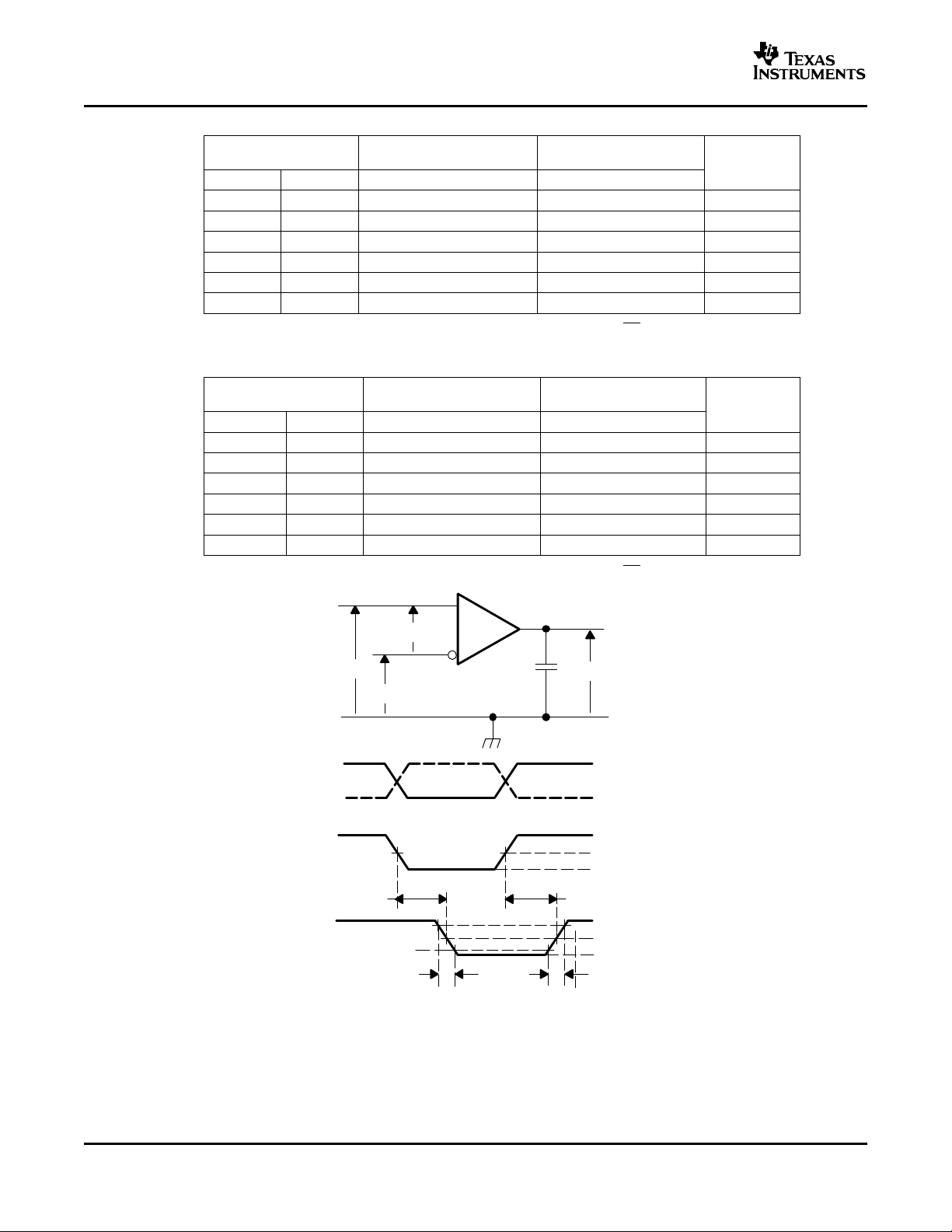
PARAMETER MEASUREMENT INFORMATION (continued)
Figure 7. Maximum Steady State Output Voltage
SN65MLVD200A , SN65MLVD202A
SN65MLVD204A , SN65MLVD205A
SLLS573 – DECEMBER 2003
A. All input pulses are supplied by an Agilent 81250 Stimulus System.
B. The measurement is made on a TEK TDS6604 running TDSJIT3 application software
C. Period jitter is measured using a 50 MHz 50 ± 1% duty cycle clock input.
D. Peak-to-peak jitter is measured using a 100Mbps 215–1 PRBS input.
Figure 8. Driver Jitter Measurement Waveforms
Figure 9. Receiver Voltage and Current Definitions
Submit Documentation Feedback
9
www.ti.com
1.2 V
1.0 V
t
pLH
0.2 V
-0.2 V
V
A
V
B
V
ID
90%
V
OH
V
OL
t
pHL
10%
t
f
t
r
V
O
VCC/2
V
O
V
ID
V
B
V
A
C
L
0 V
15 pF
SN65MLVD200A , SN65MLVD202A
SN65MLVD204A , SN65MLVD205A
SLLS573 – DECEMBER 2003
Table 1. Type-1 Receiver Input Threshold Test Voltages
APPLIED VOLTAGES
V
IA
V
2.400 0.000 2.400 1.200 H
0.000 2.400 –2.400 1.200 L
3.425 3.335 0.050 3.4 H
3.375 3.425 –0.050 3.4 L
–0.975 –1.025 0.050 –1 H
–1.025 –0.975 –0.050 –1 L
(1) H= high level, L = low level, output state assumes receiver is enabled ( RE = L)
RESULTING DIFFERENTIAL RESULTING COMMON-
INPUT VOLTAGE MODE INPUT VOLTAGE
IB
V
ID
V
IC
Table 2. Type-2 Receiver Input Threshold Test Voltages
APPLIED VOLTAGES
V
IA
V
2.400 0.000 2.400 1.200 H
0.000 2.400 –2.400 1.200 L
3.475 3.325 0.150 3.4 H
3.425 3.375 0.050 3.4 L
–0.925 –1.075 0.150 –1 H
–0.975 –1.025 0.050 –1 L
(1) H= high level, L = low level, output state assumes receiver is enabled ( RE = L)
RESULTING DIFFERENTIAL RESULTING COMMON-
INPUT VOLTAGE MODE INPUT VOLTAGE
IB
V
ID
V
IC
RECEIVER
(1)
OUTPUT
RECEIVER
OUTPUT
(1)
A. All input pulses are supplied by a generator having the following characteristics: tror tf≤ 1 ns, frequency = 1 MHz,
duty cycle = 50 ± 5%. CLis a combination of a 20%-tolerance, low-loss ceramic, surface-mount capacitor and fixture
capacitance within 2 cm of the D.U.T.
B. The measurement is made on test equipment with a –3 dB bandwidth of at least 1 GHz.
Figure 10. Receiver Timing Test Circuit and Waveforms
10
Submit Documentation Feedback

www.ti.com
15 pF
t
pZL
t
pLZ
V
OL
VOL +0.5 V
V
O
R
L
499 Ω
_
+
V
TEST
B
A
RE
1.2 V
Inputs
V
CC
1 V
V
CC
VCC/2
0 V
V
CC
VCC/2
V
TEST
A
RE
R
0 V
1.4 V
A
t
pZH
t
pHZ
0 V
VOH -0.5 V
V
CC
VCC/2
0 V
V
OH
VCC/2
RE
V
O
R
Output
V
TEST
C
L
SN65MLVD200A , SN65MLVD202A
SN65MLVD204A , SN65MLVD205A
SLLS573 – DECEMBER 2003
A. All input pulses are supplied by a generator having the following characteristics: tror tf≤ 1 ns, frequency = 1 MHz,
duty cycle = 50 ± 5%.
B. RLis 1% tolerance, metal film, surface mount, and located within 2 cm of the D.U.T.
C. CLis the instrumentation and fixture capacitance within 2 cm of the DUT and ± 20%.
Figure 11. Receiver Enable/Disable Time Test Circuit and Waveforms
Submit Documentation Feedback
11
www.ti.com
t
c(n)
1/f0
Period Jitter
Peak to Peak Jitter
1/f0
PRBS INPUT
OUTPUT
CLOCK INPUT
IDEAL
OUTPUT
ACTUAL
OUTPUT
t
jit(per)
= t
c(n)
-1/f0
t
jit(pp)
VA -V
B
INPUTS
VA -V
B
0.2 V - Type 1
0.4 V - Type 2
V
IC
1 V
V
OH
VCC/2
V
OL
V
OH
V
OL
VCC/2
V
OH
V
OL
VCC/2
V
A
V
B
SN65MLVD202AD (Marked as MLVD202A)
SN65MLVD205AD (Marked as MLVD205A)
(TOP VIEW)
1
2
3
4
5
6
7
14
13
12
11
10
9
8
NC
R
RE
DE
D
GND
GND
V
CC
V
CC
A
B
Z
Y
NC
NC - No internal connection
1
2
3
4
8
7
6
5
R
RE
DE
D
V
CC
B
A
GND
SN65MLVD200AD (Marked as MF200A)
SN65MLVD204AD (Marked as MF204A)
(TOP VIEW)
SN65MLVD200A , SN65MLVD202A
SN65MLVD204A , SN65MLVD205A
SLLS573 – DECEMBER 2003
A. All input pulses are supplied by an Agilent 8304A Stimulus System.
B. The measurement is made on a TEK TDS6604 running TDSJIT3 application software
C. Period jitter is measured using a 50 MHz 50 ±1% duty cycle clock input.
D. Peak-to-peak jitter is measured using a 100 Mbps 215-1 PRBS input.
Figure 12. Receiver Jitter Measurement Waveforms
12
PIN ASSIGNMENTS
Submit Documentation Feedback
www.ti.com
DEVICE FUNCTION TABLES
INPUTS OUTPUT
VID = VA - V
B
L
H
-50 mV < VID < 50 mV
L ?
VID ≤ -50 mV
L L
X
H Z
TYPE-1 RECEIVER (200A, 202A)
VID ≥ 50 mV
Open Circuit
L
RE
?
R
TYPE-2 RECEIVER (204A, 205A)
H = high level, L = low level, Z = high impedance, X = Don’t care, ? = indeterminate
INPUT OUTPUTS
L
H
OPEN
X
X
DRIVER
D DE A OR Y
H
H
H
OPEN
L
L
H
L
Z
Z
H
L
H
Z
Z
ENABLE
B OR Z
X
Open
Z
INPUTS OUTPUT
VID = VA - V
B
L
H
50 mV < VID < 150 mV
L ?
VID ≤ 50 mV
L L
X
H Z
VID ≥ 150 mV
Open Circuit
L
RE
L
R
X
Open
Z
360 kΩ
400 Ω
V
CC
DRIVER INPUT AND DRIVER ENABLE
D or DE
7 V
400 Ω
V
CC
RE
7 V
RECEIVER ENABLE
V
CC
7 V
10 Ω
10 Ω
RECEIVER OUTPUT
360 kΩ
DRIVER OUTPUT
A/Y or B/Z
R
V
CC
200 kΩ
250 kΩ
200 kΩ
250 kΩ
100 kΩ100 kΩ
V
CC
RECEIVER INPUT
BA
SN65MLVD200A , SN65MLVD202A
SN65MLVD204A , SN65MLVD205A
SLLS573 – DECEMBER 2003
EQUIVALENT INPUT AND OUTPUT SCHEMATIC DIAGRAMS
Submit Documentation Feedback
13

www.ti.com
0
5
10
15
20
25
30
−40 −15 10 35 60 85
I − Supply Current − mA
CC
TA − Free-Air Temperature − °C
VCC = 3.3 V
f = 50 MHz
VID = 200 mV
VIC = 1 V
Rx
Tx
0
5
10
15
20
10 20 30 40 50
I
f − Frequency − MHz
− Supply Current − mA
CC
Tx
Rx
VCC = 3.3 V
VID = 200 mV
VIC = 1 V
TA = 25°C
−90
−60
−50
−40
−30
−20
0 1 2 4
− Receiver High Level Output Current − mA
VOH − High Level Output Voltage − V
3
I
OH
−80
−70
VCC = 3.0 V
−10
0
VCC = 3.6 V
VCC = 3.3 V
TA = 25°C
0
30
40
50
60
70
0 1 2 4
− Receiver Low Level Output Current − mA
VOL − Low Level Output Voltage − V
3
I
OL
10
20
VCC = 3.6 V
VCC = 3.3 V
VCC = 3.0 V
TA = 25°C
SN65MLVD200A , SN65MLVD202A
SN65MLVD204A , SN65MLVD205A
SLLS573 – DECEMBER 2003
TYPICAL CHARACTERISTICS
SUPPLY CURRENT SUPPLY CURRENT
RECEIVER LOW-LEVEL OUTPUT CURRENT RECEIVER HIGH-LEVEL OUTPUT CURRENT
LOW-LEVEL OUTPUT VOLTAGE HIGH-LEVEL OUTPUT VOLTAGE
vs vs
FREQUENCY FREE-AIR TEMPERATURE
Figure 13. Figure 14.
vs vs
14
Figure 15. Figure 16.
Submit Documentation Feedback

www.ti.com
3
3.20
3.40
3.60
3.80
4
−40 −15 10 35 60 85
Receiver Propagation Delay − ns
TA − Free-Air Temperature − °C
VCC = 3.3 V
VID = 200 mV
VIC = 1 V
f = 1 MHz
CL = 15 pF
t
pLH
t
pHL
2
2.2
2.4
2.6
2.8
−40 −15 10 35 60 85
Driver Propagation Delay − ns
TA − Free-Air Temperature − °C
VCC = 3.3 V
f = 1 MHz
RL = 50 Ω
t
pHL
t
pLH
20
28
36
44
52
60
20 40 60 80 100
Signaling Rate − Mbps
Added Driver Peak-To-Peak Jitter − ps
VCC = 3.3 V
TA = 25°C
215-1 PRBS NRZ
0
6
12
18
24
30
10 20 30 40 50
Clock Frequency − MHz
Added Driver Cycle-To-Cycle Jitter − ps
VCC = 3.3 V
TA = 25°C
Input = Clock
TYPICAL CHARACTERISTICS (continued)
SN65MLVD200A , SN65MLVD202A
SN65MLVD204A , SN65MLVD205A
SLLS573 – DECEMBER 2003
DRIVER PROPAGATION DELAY RECEIVER PROPAGATION DELAY
FREE-AIR TEMPERATURE FREE-AIR TEMPERATURE
ADDED DRIVER CYCLE-TO-CYCLE JITTER ADDED DRIVER PEAK-TO-PEAK JITTER
CLOCK FREQUENCY SIGNALING RATE
vs vs
Figure 17. Figure 18.
vs vs
Figure 19. Figure 20.
Submit Documentation Feedback
15

www.ti.com
10
16
22
28
34
40
10 20 30 40 50
Clock Frequency − MHz
Added Receiver Cycle-To-Cycle Jitter − ps
VCC = 3.3 V
TA = 25°C
VIC = 1 V
Type-1
VID = 200 mV
Type-2
VID = 400 mV
40
48
56
64
72
80
−40 −15 10 35 60 85
Added Driver Peak-To-Peak Jitter − ps
TA − Free-Air Temperature − °C
VCC = 3.3 V
V
IC
= 1 V
f = 100 Mbps
215-1 PRBS NRZ
0
60
120
180
240
300
20 40 60 80 100
Added Receiver Peak-To-Peak Jitter − ps
Signaling Rate − Mbps
Type-2
VID = 400 mV
Type-1
VID = 200 mV
VCC = 3.3 V
TA = 25C
VIC = 1 V
215-1 PRBS NRZ
0
60
120
180
240
300
−40 −15 10 35 60 85
TA − Free-Air Temperature − °C
Added Receiver Peak-To-Peak Jitter − ps
Type-2
VID = 400 mV
Type-1
VID = 200 mV
VCC = 3.3 V
VIC = 1 V
215-1 PRBS NRZ
SN65MLVD200A , SN65MLVD202A
SN65MLVD204A , SN65MLVD205A
SLLS573 – DECEMBER 2003
TYPICAL CHARACTERISTICS (continued)
ADDED DRIVER PEAK-TO-PEAK JITTER ADDED RECEIVER CYCLE-TO-CYCLE JITTER
FREE-AIR TEMPERATURE CLOCK FREQUENCY
ADDED RECEIVER PEAK-TO-PEAK JITTER ADDED RECEIVER PEAK-TO-PEAK JITTER
vs vs
Figure 21. Figure 22.
vs vs
SIGNALING RATE FREE-AIR TEMPERATURE
16
Figure 23. Figure 24.
Submit Documentation Feedback

www.ti.com
Horizontal Scale = 2 ns/div
Vertical Scale = 127.2 mV/div
Horizontal Scale = 2 ns/div
Vertical Scale = 400 mV/div
TYPICAL CHARACTERISTICS (continued)
SN65MLVD200A DRIVER OUTPUT EYE PATTERN
vs
100 Mbps, 2
SN65MLVD200A RECEIVER OUTPUT EYE PATTERN
100 Mbps, 2
15-1
Figure 25.
vs
15-1
SN65MLVD200A , SN65MLVD202A
SN65MLVD204A , SN65MLVD205A
SLLS573 – DECEMBER 2003
PRBS, RL= 50 Ω
PRBS, cL= 15 pF
Submit Documentation Feedback
Figure 26.
17

www.ti.com
-100
-50
0
50
100
150
200
Type 1
Transition Regions
Type 2
Low
High
Low
High
- Differential Input Voltage - mV
V
ID
SN65MLVD200A , SN65MLVD202A
SN65MLVD204A , SN65MLVD205A
SLLS573 – DECEMBER 2003
APPLICATION INFORMATION
COMPARISON OF MLVD TO TIA/EIA-485
Receiver Input Threshold (Failsafe)
The MLVD standard defines a type 1 and type 2 receiver. Type 1 receivers include no provisions for failsafe and
have their differential input voltage thresholds near zero volts. Type 2 receivers have their differential input
voltage thresholds offset from zero volts to detect the absence of a voltage difference. The impact to receiver
output by the offset input can be seen in Table 3 and Figure 27 .
Table 3. Receiver Input Voltage Threshold Requirements
RECEIVER TYPE OUTPUT LOW OUTPUT HIGH
Type 1 –2.4 V ≤ VID≤ -0.05 V 0.05 V ≤ VID≤ 2.4 V
Type 2 –2.4 V ≤ VID≤ 0.05 V 0.15 V ≤ VID≤ 2.4 V
Figure 27. Expanded Graph of Receiver Differential Input Voltage Showing Transition Region
18
Submit Documentation Feedback

PACKAGE OPTION ADDENDUM
www.ti.com
8-Jan-2007
PACKAGING INFORMATION
Orderable Device Status
(1)
Package
Type
Package
Drawing
Pins Package
Qty
Eco Plan
SN65MLVD200AD ACTIVE SOIC D 8 75 Green (RoHS &
no Sb/Br)
SN65MLVD200ADG4 ACTIVE SOIC D 8 75 Green (RoHS &
no Sb/Br)
SN65MLVD200ADR ACTIVE SOIC D 8 2500 Green (RoHS &
no Sb/Br)
SN65MLVD200ADRG4 ACTIVE SOIC D 8 2500 Green (RoHS &
no Sb/Br)
SN65MLVD202AD ACTIVE SOIC D 14 50 Green (RoHS &
no Sb/Br)
SN65MLVD202ADG4 ACTIVE SOIC D 14 50 Green (RoHS &
no Sb/Br)
SN65MLVD202ADR ACTIVE SOIC D 14 2500 Green (RoHS &
no Sb/Br)
SN65MLVD202ADRG4 ACTIVE SOIC D 14 2500 Green (RoHS &
no Sb/Br)
SN65MLVD204AD ACTIVE SOIC D 8 75 Green (RoHS &
no Sb/Br)
SN65MLVD204ADG4 ACTIVE SOIC D 8 75 Green (RoHS &
no Sb/Br)
SN65MLVD204ADR ACTIVE SOIC D 8 2500 Green (RoHS &
no Sb/Br)
SN65MLVD204ADRG4 ACTIVE SOIC D 8 2500 Green (RoHS &
no Sb/Br)
SN65MLVD205AD ACTIVE SOIC D 14 50 Green (RoHS &
no Sb/Br)
SN65MLVD205ADG4 ACTIVE SOIC D 14 50 Green (RoHS &
no Sb/Br)
SN65MLVD205ADR ACTIVE SOIC D 14 2500 Green (RoHS &
no Sb/Br)
SN65MLVD205ADRG4 ACTIVE SOIC D 14 2500 Green (RoHS &
no Sb/Br)
(1)
The marketing status values are defined as follows:
ACTIVE: Product device recommended for new designs.
LIFEBUY: TI has announced that the device will be discontinued, and a lifetime-buy period is in effect.
NRND: Not recommended for new designs. Device is in production to support existing customers, but TI does not recommend using this part in
a new design.
PREVIEW: Device has been announced but is not in production. Samples may or may not be available.
OBSOLETE: TI has discontinued the production of the device.
(2)
Lead/Ball Finish MSL Peak Temp
CU NIPDAU Level-1-260C-UNLIM
CU NIPDAU Level-1-260C-UNLIM
CU NIPDAU Level-1-260C-UNLIM
CU NIPDAU Level-1-260C-UNLIM
CU NIPDAU Level-1-260C-UNLIM
CU NIPDAU Level-1-260C-UNLIM
CU NIPDAU Level-1-260C-UNLIM
CU NIPDAU Level-1-260C-UNLIM
CU NIPDAU Level-1-260C-UNLIM
CU NIPDAU Level-1-260C-UNLIM
CU NIPDAU Level-1-260C-UNLIM
CU NIPDAU Level-1-260C-UNLIM
CU NIPDAU Level-1-260C-UNLIM
CU NIPDAU Level-1-260C-UNLIM
CU NIPDAU Level-1-260C-UNLIM
CU NIPDAU Level-1-260C-UNLIM
(3)
(2)
Eco Plan - The planned eco-friendly classification: Pb-Free (RoHS), Pb-Free (RoHS Exempt), or Green (RoHS & no Sb/Br) - please check
http://www.ti.com/productcontent for the latest availability information and additional product content details.
TBD: The Pb-Free/Green conversion plan has not been defined.
Pb-Free (RoHS): TI's terms "Lead-Free" or "Pb-Free" mean semiconductor products that are compatible with the current RoHS requirements
for all 6 substances, including the requirement that lead not exceed 0.1% by weight in homogeneous materials. Where designed to be soldered
at high temperatures, TI Pb-Free products are suitable for use in specified lead-free processes.
Pb-Free (RoHS Exempt): This component has a RoHS exemption for either 1) lead-based flip-chip solder bumps used between the die and
package, or 2) lead-based die adhesive used between the die and leadframe. The component is otherwise considered Pb-Free (RoHS
compatible) as defined above.
Green (RoHS & no Sb/Br): TI defines "Green" to mean Pb-Free (RoHS compatible), and free of Bromine (Br) and Antimony (Sb) based flame
retardants (Br or Sb do not exceed 0.1% by weight in homogeneous material)
Addendum-Page 1

PACKAGE OPTION ADDENDUM
www.ti.com
(3)
MSL, Peak Temp. -- The Moisture Sensitivity Level rating according to the JEDEC industry standard classifications, and peak solder
temperature.
Important Information and Disclaimer:The information provided on this page represents TI's knowledge and belief as of the date that it is
provided. TI bases its knowledge and belief on information provided by third parties, and makes no representation or warranty as to the
accuracy of such information. Efforts are underway to better integrate information from third parties. TI has taken and continues to take
reasonable steps to provide representative and accurate information but may not have conducted destructive testing or chemical analysis on
incoming materials and chemicals. TI and TI suppliers consider certain information to be proprietary, and thus CAS numbers and other limited
information may not be available for release.
In no event shall TI's liability arising out of such information exceed the total purchase price of the TI part(s) at issue in this document sold by TI
to Customer on an annual basis.
8-Jan-2007
Addendum-Page 2
PACKAGE MATERIALS INFORMATION
www.ti.com
16-Jun-2007
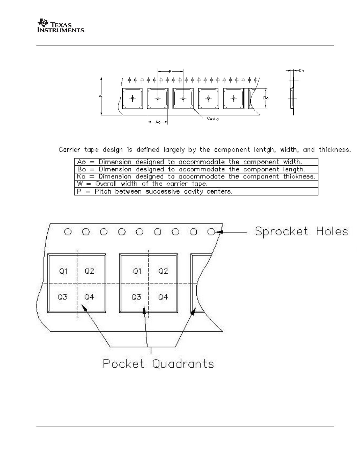
TAPE AND REEL INFORMATION
Pack Materials-Page 1

PACKAGE MATERIALS INFORMATION
www.ti.com
Device Package Pins Site Reel
Diameter
(mm)
SN65MLVD200ADR D 8 FMX 330 0 6.4 5.2 2.1 8 12 Q1
SN65MLVD202ADR D 14 FMX 330 0 6.5 9.0 2.1 8 16 Q1
SN65MLVD204ADR D 8 FMX 330 0 6.4 5.2 2.1 8 12 Q1
SN65MLVD205ADR D 14 FMX 330 0 6.5 9.0 2.1 8 16 Q1
Reel
Width
(mm)
A0 (mm) B0 (mm) K0 (mm) P1
(mm)W(mm)
16-Jun-2007
Pin1
Quadrant
TAPE AND REEL BOX INFORMATION
Device Package Pins Site Length (mm) Width (mm) Height (mm)
SN65MLVD200ADR D 8 FMX 342.9 336.6 20.6
SN65MLVD202ADR D 14 FMX 342.9 336.6 28.58
SN65MLVD204ADR D 8 FMX 342.9 336.6 20.6
SN65MLVD205ADR D 14 FMX 342.9 336.6 28.58
Pack Materials-Page 2

PACKAGE MATERIALS INFORMATION
www.ti.com
16-Jun-2007
Pack Materials-Page 3


IMPORTANT NOTICE
Texas Instruments Incorporated and its subsidiaries (TI) reserve the right to make corrections, modifications, enhancements,
improvements, and other changes to its products and services at any time and to discontinue any product or service without notice.
Customers should obtain the latest relevant information before placing orders and should verify that such information is current and
complete. All products are sold subject to TI’s terms and conditions of sale supplied at the time of order acknowledgment.
TI warrants performance of its hardware products to the specifications applicable at the time of sale in accordance with TI’s
standard warranty. Testing and other quality control techniques are used to the extent TI deems necessary to support this
warranty. Except where mandated by government requirements, testing of all parameters of each product is not necessarily
performed.
TI assumes no liability for applications assistance or customer product design. Customers are responsible for their products and
applications using TI components. To minimize the risks associated with customer products and applications, customers should
provide adequate design and operating safeguards.
TI does not warrant or represent that any license, either express or implied, is granted under any TI patent right, copyright, mask
work right, or other TI intellectual property right relating to any combination, machine, or process in which TI products or services
are used. Information published by TI regarding third-party products or services does not constitute a license from TI to use such
products or services or a warranty or endorsement thereof. Use of such information may require a license from a third party under
the patents or other intellectual property of the third party, or a license from TI under the patents or other intellectual property of TI.
Reproduction of TI information in TI data books or data sheets is permissible only if reproduction is without alteration and is
accompanied by all associated warranties, conditions, limitations, and notices. Reproduction of this information with alteration is an
unfair and deceptive business practice. TI is not responsible or liable for such altered documentation. Information of third parties
may be subject to additional restrictions.
Resale of TI products or services with statements different from or beyond the parameters stated by TI for that product or service
voids all express and any implied warranties for the associated TI product or service and is an unfair and deceptive business
practice. TI is not responsible or liable for any such statements.
TI products are not authorized for use in safety-critical applications (such as life support) where a failure of the TI product would
reasonably be expected to cause severe personal injury or death, unless officers of the parties have executed an agreement
specifically governing such use. Buyers represent that they have all necessary expertise in the safety and regulatory ramifications
of their applications, and acknowledge and agree that they are solely responsible for all legal, regulatory and safety-related
requirements concerning their products and any use of TI products in such safety-critical applications, notwithstanding any
applications-related information or support that may be provided by TI. Further, Buyers must fully indemnify TI and its
representatives against any damages arising out of the use of TI products in such safety-critical applications.
TI products are neither designed nor intended for use in military/aerospace applications or environments unless the TI products are
specifically designated by TI as military-grade or "enhanced plastic." Only products designated by TI as military-grade meet military
specifications. Buyers acknowledge and agree that any such use of TI products which TI has not designated as military-grade is
solely at the Buyer's risk, and that they are solely responsible for compliance with all legal and regulatory requirements in
connection with such use.
TI products are neither designed nor intended for use in automotive applications or environments unless the specific TI products
are designated by TI as compliant with ISO/TS 16949 requirements. Buyers acknowledge and agree that, if they use any
non-designated products in automotive applications, TI will not be responsible for any failure to meet such requirements.
Following are URLs where you can obtain information on other Texas Instruments products and application solutions:
Products Applications
Amplifiers amplifier.ti.com Audio www.ti.com/audio
Data Converters dataconverter.ti.com Automotive www.ti.com/automotive
DSP dsp.ti.com Broadband www.ti.com/broadband
Interface interface.ti.com Digital Control www.ti.com/digitalcontrol
Logic logic.ti.com Military www.ti.com/military
Power Mgmt power.ti.com Optical Networking www.ti.com/opticalnetwork
Microcontrollers microcontroller.ti.com Security www.ti.com/security
RFID www.ti-rfid.com Telephony www.ti.com/telephony
Low Power www.ti.com/lpw Video & Imaging www.ti.com/video
Wireless
Wireless www.ti.com/wireless
Mailing Address: Texas Instruments, Post Office Box 655303, Dallas, Texas 75265
Copyright © 2007, Texas Instruments Incorporated
 Loading...