

查询SN65HVD230QD供应商
SN65HVD230Q-Q1
SN65HVD231Q-Q1
SN65HVD232Q-Q1
SGLS117C – JUNE 2001 – REVISED JUNE 2002
3.3-V CAN TRANSCEIVERS
FEATURES
D Qualification in Accordance With AEC-Q100
†
D Qualified for Automotive Applications
D Customer-Specific Configuration Control Can
Be Supported Along With Major-Change
Approval
D ESD Protection Exceeds 2000 V Per
MIL-STD-883, Method 3015; Exceeds 200 V
Using Machine Model (C = 200 pF, R = 0)
D Operates With a 3.3-V Supply
D Low Power Replacement for the PCA82C250
Footprint
D Bus/Pin ESD Protection Exceeds 15-kV HBM
D Controlled Driver Output Transition Times for
Improved Signal Quality on the SN65HVD230Q
and SN65HVD231Q
D Unpowered Node Does Not Disturb the Bus
D Compatible With the Requirements of the
ISO 11898 Standard
D Low-Current SN65HVD230Q Standby Mode
370 µA Typical
†
Contact factory for details. Q100 qualification data available on
request.
D Low-Current SN65HVD231Q Sleep Mode
0.1 µA Typical
D Designed for Signaling Rates
‡
Up To
1 Megabit/Second (Mbps)
D Thermal Shutdown Protection
D Open-Circuit Fail-Safe Design
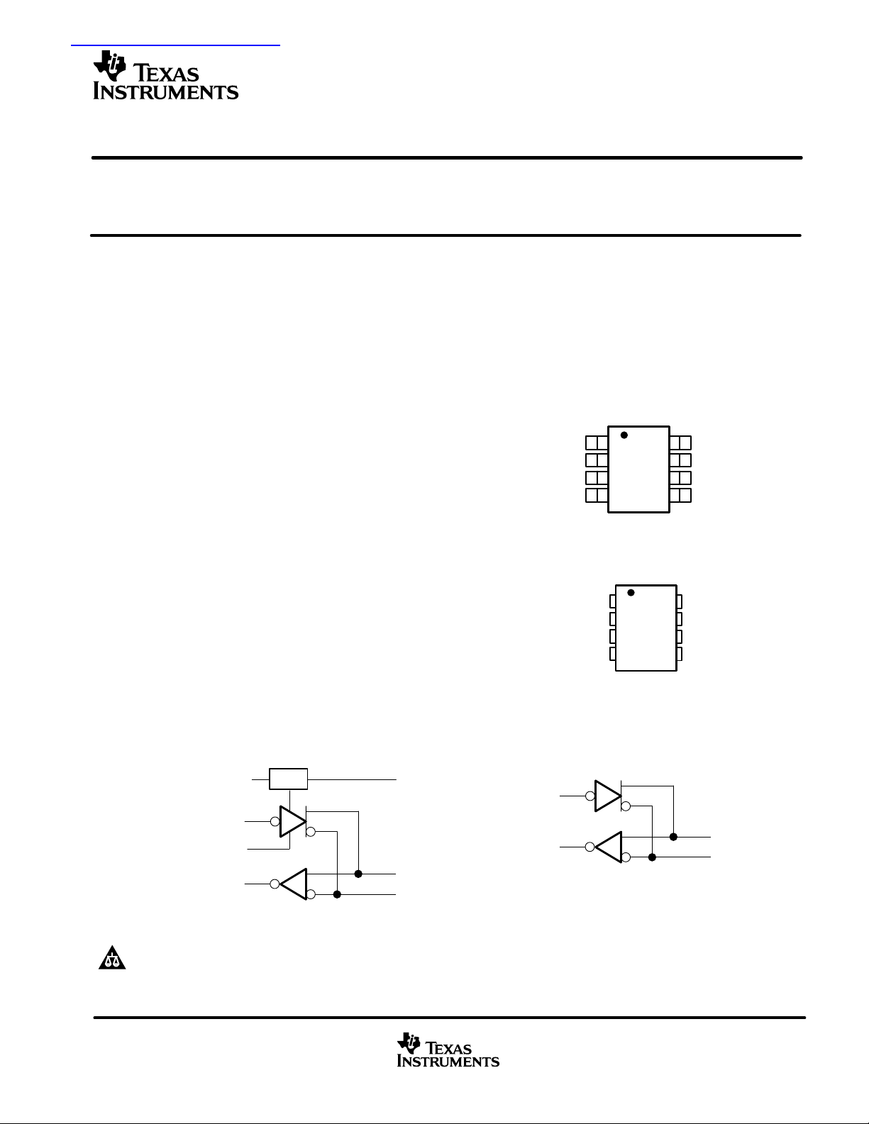
SN65HVD230QD
SN65HVD231QD
(TOP VIEW)
GND
V
CC
D
R
1
2
3
4
SN65HVD232QD
(TOP VIEW)
D
1
GND
V
NC – No internal connection
CC
2
3
4
R
R
8
7
6
5
8
7
6
5
S
CANH
CANL
V
ref
NC
CANH
CANL
NC
logic diagram (positive logic)
SN65HVD230Q, SN65HVD231Q
Logic Diagram (Positive Logic)
3
V
CC
1
D
8
R
S
4
R
Please be aware that an important notice concerning availability , standard warranty , and use in critical applications of T exas Instruments
semiconductor products and disclaimers thereto appears at the end of this data sheet.
‡
The signaling rate of a line is the number of voltage transitions that are made per second expressed in the units bps (bits per second).
PRODUCTION DATA information is current as of publication date.
Products conform to specifications per the terms of Texas Instruments
standard warranty. Production processing does not necessarily include
testing of all parameters.
5
7
6
V
ref
CANH
CANL
www.ti.com
Logic Diagram (Positive Logic)
D
R
SN65HVD232Q
1
7
4
Copyright 2002, Texas Instruments Incorporated
CANH
6
CANL
1
SN65HVD230Q-Q1
125°C
125°C
SN65HVD231Q-Q1
SN65HVD232Q-Q1
SGLS117C – JUNE 2001 – REVISED JUNE 2002
DESCRIPTION
The SN65HVD230Q, SN65HVD231Q, and SN65HVD232Q controller area network (CAN) transceivers are
designed for use with the Texas Instruments TMS320Lx240x 3.3-V DSPs with CAN controllers, or with
equivalent devices. They are intended for use in applications employing the CAN serial communication physical
layer in accordance with the ISO 11898 standard. Each CAN transceiver is designed to provide differential
transmit capability to the bus and differential receive capability to a CAN controller at speeds up to 1 Mbps.
Designed for operation in especially-harsh environments, these devices feature cross-wire protection,
loss-of-ground and overvoltage protection, overtemperature protection, as well as wide common-mode range.
The transceiver interfaces the single-ended CAN controller with the differential CAN bus found in industrial,
building automation, and automotive applications. It operates over a –2-V to 7-V common-mode range on the
bus, and it can withstand common-mode transients of ±25 V.
On the SN65HVD230Q and SN65HVD231Q, R
(pin 8) provides three different modes of operation:
S
high-speed, slope control, and low-power modes. The high-speed mode of operation is selected by connecting
pin 8 to ground, allowing the transmitter output transistors to switch on and off as fast as possible with no
limitation on the rise and fall slopes. The rise and fall slopes can be adjusted by connecting a resistor to ground
at pin 8, since the slope is proportional to the pin’s output current. This slope control is implemented with external
resistor values of 10 kΩ, to achieve a 15-V/µs slew rate, to 100 kΩ, to achieve a 2-V/µs slew rate.
The circuit of the SN65HVD230Q enters a low-current standby mode during which the driver is switched off and
the receiver remains active if a high logic level is applied to R
(pin 8). The DSP controller reverses this
S
low-current standby mode when a dominant state (bus differential voltage > 900 mV typical) occurs on the bus.
The unique difference between the SN65HVD230Q and the SN65HVD231Q is that both the driver and the
receiver are switched off in the SN65HVD231Q when a high logic level is applied to R
this sleep mode until the circuit is reactivated by a low logic level on R
The V
(pin 5 on the SN65HVD230Q and SN65HVD231Q) is available as a VCC/2 voltage reference.
ref
.
S
(pin 8) and remain in
S
The SN65HVD232Q is a basic CAN transceiver with no added options; pins 5 and 8 are NC, no connection.
AVAILABLE OPTIONS
FUNCTION
NUMBER
’230 370-µA standby mode Yes Yes
’231 10-µA sleep mode Yes Yes
’232 No standby or sleep mode No No
PART NUMBER Q100 T
SN65HVD230QD No
SN65HVD231QD No
SN65HVD232QD No
SN65HVD230QDQ1 Yes
SN65HVD231QDQ1 Yes
SN65HVD232QDQ1 Yes
The D package is available taped and reeled. Add the suffix R to device type (e.g.,
SN65HVD230QDRQ1).
LOW
POWER MODE
INTEGRATED SLOPE
CONTROL
A
–40°C to
°
–40°C to
°
MARKED AS:
Vref PIN
HV230Q
HV231Q
HV232Q
230Q1
231Q1
232Q1
2
www.ti.com
(Rs)
V
(Rs)
1.2 V
SN65HVD230Q-Q1
SN65HVD231Q-Q1
SN65HVD232Q-Q1
SGLS117C – JUNE 2001 – REVISED JUNE 2002
Function Tables
DRIVER (SN65HVD230Q, SN65HVD231Q)
INPUT D R
L
H
Open X Z Z Recessive
X V
H = high level; L = low level; X = irrelevant; ? = indeterminate
INPUT D
L H L Dominant
H Z Z Recessive
Open Z Z Recessive
H = high level; L = low level
DIFFERENTIAL INPUTS
VID ≥ 0.9 V X L
0.5 V < VID < 0.9 V X ?
VID ≤ 0.5 V X H
Open X H
H = high level; L = low level; X = irrelevant; ? = indeterminate
DIFFERENTIAL INPUTS
VID ≥ 0.9 V L
0.5 V < VID < 0.9 V
VID ≤ 0.5 V
X V
X 1.2 V < V
Open X H
H = high level; L = low level; X = irrelevant; ? = indeterminate
DIFFERENTIAL INPUTS
VID ≥ 0.9 V L
0.5 V < VID < 0.9 V ?
VID ≤ 0.5 V H
H = high level; L = low level; X = irrelevant; ? = indeterminate
S
V
< 1.2 V
(Rs)
> 0.75 V
(Rs)
DRIVER (SN65HVD232Q)
RECEIVER (SN65HVD230Q)
RECEIVER (SN65HVD231Q)
RECEIVER (SN65HVD232Q)
Open H
CC
OUTPUTS
CANH CANL
OUTPUTS
CANH CANL
H L Dominant
Z Z Recessive
Z Z Recessive
BUS STATE
V
(Rs)
R
S
R
S
< 1.2 V
<
> 0.75 V
< 0.75 V
(Rs)
OUTPUT R
CC
CC
OUTPUT R
BUS STATE
OUTPUT R
?
H
H
?
www.ti.com
3
SN65HVD230Q-Q1
SN65HVD231Q-Q1
SN65HVD232Q-Q1
SGLS117C – JUNE 2001 – REVISED JUNE 2002
TRANSCEIVER MODES (SN65HVD230Q, SN65HVD231Q)
V
10 kΩ to 100 kΩ to ground Slope control
TERMINAL
NAME NO.
CANL 6 Low bus output
CANH 7 High bus output
D 1 Driver input
GND 2 Ground
R 4 Receiver output
R
S
V
CC
V
ref
Function Tables (Continued)
V
(Rs)
> 0.75 V
(RS)
V
(RS)
CC
< 1 V High speed (no slope control)
OPERATING MODE
Standby
Terminal Functions
SN65HVD230Q, SN65HVD231Q
DESCRIPTION
8 Standby/slope control
3 Supply voltage
5 Reference output
SN65HVD232Q
TERMINAL
NAME NO.
CANL 6 Low bus output
CANH 7 High bus output
D 1 Driver input
GND 2 Ground
NC 5, 8 No connection
R 4 Receiver output
V
CC
3 Supply voltage
DESCRIPTION
4
www.ti.com
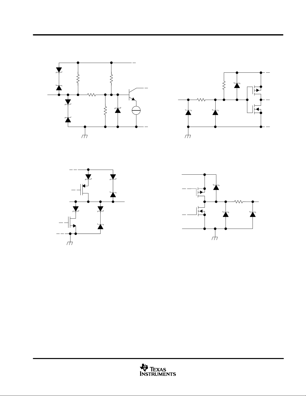
equivalent input and output schematic diagrams
SN65HVD230Q-Q1
SN65HVD231Q-Q1
SN65HVD232Q-Q1
SGLS117C – JUNE 2001 – REVISED JUNE 2002
Input
16 V
20 V
CANH and CANL Inputs
110 kΩ
45 kΩ
CANH and CANL Outputs
V
CC
9 kΩ
9 kΩ
16 V
D Input
V
CC
V
CC
100 kΩ
Input
V
CC
1 kΩ
9 V
R Output
20 V
Output
5 Ω
Output
9 V
www.ti.com
5
SN65HVD230Q-Q1
SN65HVD231Q-Q1
SN65HVD232Q-Q1
SGLS117C – JUNE 2001 – REVISED JUNE 2002
absolute maximum ratings over operating free-air temperature (see Note 1) (unless otherwise
noted)
Supply voltage range, V
Voltage range at any bus terminal (CANH or CANL) –7 V to 16 V. . . . . . . . . . . . . . . . . . . . . . . . . . . . . . . . . . . . . . . . . .
Voltage input range, transient pulse, CANH and CANL, through 100 Ω (see Figure 7) –25 V to 25 V. . . . . . . . . . . .
Input voltage range, V
Electrostatic discharge: Human body model (see Note 2) CANH, CANL and GND 15 kV. . . . . . . . . . . . . . . . . .
Continuous total power dissipation See Dissipation Rating table. . . . . . . . . . . . . . . . . . . . . . . . . . . . . . . . . . . . . . . . . . .
Storage temperature range, T
Lead temperature 1,6 mm (1/16 inch) from case for 10 seconds 260°C. . . . . . . . . . . . . . . . . . . . . . . . . . . . . . . . . . . . .
†
NOTES: 1. All voltage values, except differential I/O bus voltages, are with respect to network ground terminal.
†
CC
(D or R) –0.5 V to VCC + 0.5 V. . . . . . . . . . . . . . . . . . . . . . . . . . . . . . . . . . . . . . . . . . . . . . . . . . .
I
–0.3 V to 6 V. . . . . . . . . . . . . . . . . . . . . . . . . . . . . . . . . . . . . . . . . . . . . . . . . . . . . . . . . . . . . . .
All pins 2.5 kV. . . . . . . . . . . . . . . . . . . . . . . . . . . . . . . .
Charged-device model (see Note 3) All pins 4 kV. . . . . . . . . . . . . . . . . . . . . . . . . . . . . . . . . .
stg
Stresses beyond those listed under “absolute maximum ratings” may cause permanent damage to the device. These are stress ratings only, and
functional operation of the device at these or any other conditions beyond those indicated under “recommended operating conditions” is not
implied. Exposure to absolute-maximum-rated conditions for extended periods may affect device reliability.
2. Tested in accordance with JEDEC Standard 22, Test Method A114-A.
3. Tested in accordance with JEDEC Standard 22, Test Method C101.
DISSIPATION RATING TABLE
PACKAGE
D 725 mW 5.8 mW/°C 464 mW 377 mW 145 mW
‡
This is the inverse of the junction-to-ambient thermal resistance when board-mounted and with no air flow.
TA ≤ 25°C
POWER RATING
DERATING FACTOR
ABOVE TA = 25°C
‡
TA = 70°C
POWER RATING
TA = 85°C
POWER RATING
–65°C to 150°C. . . . . . . . . . . . . . . . . . . . . . . . . . . . . . . . . . . . . . . . . . . . . . . . . . . . . . . .
TA = 125°C
POWER RATING
recommended operating conditions
PARAMETER MIN NOM MAX UNIT
Supply voltage, V
Voltage at any bus terminal (common mode) V
Voltage at any bus terminal (separately) V
High-level input voltage, V
Low-level input voltage, V
Differential input voltage, VID (see Figure 5) –6 6 V
V
(RS)
V
for standby or sleep 0.75 V
(RS)
Rs wave-shaping resistance 0 100 kΩ
High-level output current, I
Low-level output current, I
Operating free-air temperature, T
§
The algebraic convention, in which the least positive (most negative) limit is designated as minimum is used in this data sheet.
CC
IH
IL
OL
OH
IC
I
D, R 2 V
D, R 0.8 V
Driver –40
Receiver –8
Driver 48
Receiver 8
A
3 3.6 V
§
–2
–2.5 7.5 V
0 V
CC
–40 125 °C
CC
V
CC
7 V
V
V
mA
mA
6
www.ti.com
,
V
I
Bus out ut
,
V
I
Differential out ut
t
PLH
Pro agation delay time, low to high level out ut
ns
t
PHL
Pro agation delay time, high to low level out ut
ns
(p)
(HL)
(LH)
t
sk( )
Pulse skew (|t
P(HL)
t
P(LH)
|)
S
4
ns
SN65HVD230Q-Q1
SN65HVD231Q-Q1
SN65HVD232Q-Q1
SGLS117C – JUNE 2001 – REVISED JUNE 2002
driver electrical characteristics over recommended operating conditions (unless otherwise noted)
PARAMETER TEST CONDITIONS MIN TYP†MAX UNIT
V
OH
V
OL
V
OD(D)
V
OD(R)
I
IH
I
IL
I
OS
C
o
I
CC
†
All typical values are at 25°C and with a 3.3-V supply.
Bus output
voltage
Differential output
voltage
High-level input current VI = 2 V –30 µA
Low-level input current VI = 0.8 V –30 µA
Short-circuit output current
Output capacitance See receiver
pp
Supply current
Dominant
Recessive
Dominant
Recessive
Standby SN65HVD230Q
Sleep SN65HVD231Q
All devices
Dominant VI = 0 V, No load Dominant 10 17
Recessive VI = VCC, No load Recessive 10 17
V
= 0 V
= 0 V,
See Figure 1 and Figure 3
V
= 3 V
= 3 V,
See Figure 1 and Figure 3
VI = 0 V, See Figure 1 1.5 2 3
VI = 0 V, See Figure 2 1.2 2 3
VI = 3 V, See Figure 1 –120 0 12 mV
VI = 3 V, No load –0.5 –0.2 0.05 V
V
= –2 V –250 250
CANH
V
= 7 V
CANL
V
= V
(RS)
CC
CANH 2.45 V
CANL 0.5 1.25
CANH 2.3
CANL 2.3
–250 250
370 600
0.1
CC
V
V
mA
µA
mA
driver switching characteristics at TA = 25°C (unless otherwise noted)
SN65HVD230Q and SN65HVD231Q
PARAMETER TEST CONDITIONS MIN TYP MAX UNIT
V
= 0 V 35 85
(RS)
t
PLH
t
PHL
t
sk
t
r
t
f
t
r
t
f
t
r
t
f
Propagation delay time, low-to-high-level output
Propagation delay time, high-to-low-level output
Pulse skew (|t
Differential output signal rise time
Differential output signal fall time
Differential output signal rise time
Differential output signal fall time
Differential output signal rise time
Differential output signal fall time
– t
P
|)
P
RS with 10 kΩ to ground 70 125
RS with 100 kΩ to ground 500 870
V
= 0 V 70 120
(RS)
RS with 10 kΩ to ground
RS with 100 kΩ to ground 870 1200
V
= 0 V 35
(RS)
RS with 10 kΩ to ground
RS with 100 kΩ to ground
V
= 0 V
(RS)
RS with 10 kΩ to ground
RS with 100 kΩ to ground
CL = 50 pF,
ee Figure
ns
130 180
60
370
25 50 100 ns
40 55 80 ns
80 120 160 ns
80 125 150 ns
600 800 1200 ns
600 825 1000 ns
ns
ns
www.ti.com
7
SN65HVD230Q-Q1
C
L
See Figure 4
V
Other in ut at 0 V
See Figure 6
SN65HVD231Q-Q1
SN65HVD232Q-Q1
SGLS117C – JUNE 2001 – REVISED JUNE 2002
driver switching characteristics at TA = 25°C (unless otherwise noted)
SN65HVD232Q
PARAMETER TEST CONDITIONS MIN TYP MAX UNIT
t
PLH
t
PHL
t
sk(p)
t
r
t
f
receiver electrical characteristics over recommended operating conditions (unless otherwise
noted)
V
V
V
V
V
I
I
C
C
R
R
I
CC
†
All typical values are at 25°C and with a 3.3-V supply.
Propagation delay time, low-to-high-level output 35 85 ns
Propagation delay time, high-to-low-level output 70 120 ns
Pulse skew (|t
Differential output signal rise time
Differential output signal fall time 40 55 80 ns
PARAMETER TEST CONDITIONS MIN TYP†MAX UNIT
Positive-going input threshold voltage
IT+
Negative-going input threshold voltage
IT–
Hysteresis voltage (V
hys
High-level output voltage
OH
Low-level output voltage 900 mV ≤ VID ≤ 6 V, IO = 8 mA, See Figure 5 0.4
OL
Bus input current
CANH, CANL input capacitance
i
Differential input capacitance
diff
Differential input resistance Pin-to-pin, V
diff
T
CANH, CANL input resistance
Supply current
P(HL)
– t
P(LH)
IT+ – VIT–
|)
See Table 1
) 100
–6 V ≤ VID ≤ 500 mV, IO = –8 mA, See Figure 5
VIH = 7 V 100 250
VIH = 7 V, VCC = 0 V
VIH = –2 V
VIH = –2 V, VCC = 0 V –100 –20
Pin-to-ground,
VI = 0.4 sin(4E6πt) + 0.5 V
Pin-to-pin,
VI = 0.4 sin(4E6πt) + 0.5 V
= 3 V 40 70 100 kΩ
(D)
See driver
CL = 50 pF, See Figure 4
50 F,
Other input at 0 V ,
D = 3 V
V
= 3 V,
(D)
V
= 3 V,
(D)
25 50 100 ns
500 650
2.4
100 350
,
–200 –30
20 35 50 kΩ
35 ns
750 900 mV
32 pF
16 pF
mV
V
µA
µA
receiver switching characteristics at TA = 25°C (unless otherwise noted)
t
PLH
t
PHL
t
sk(p)
t
r
t
f
t
(loop
t
(loop)
t
(loop)
8
PARAMETER
Propagation delay time, low-to-high-level output 35 50 ns
Propagation delay time, high-to-low-level output
Pulse skew (|t
Output signal rise time
Output signal fall time
) Total loop delay, driver input to receiver output V
Total loop delay, driver input to receiver output RS with 10 kΩ to ground 105 175
Total loop delay, driver input to receiver output RS with 100 kΩ to ground 535 920
P(HL)
– t
P(LH)
|)
= 0 V 70 135
(RS)
www.ti.com
TEST
CONDITIONS
See Figure 6
See Figure 6
MIN TYP MAX UNIT
35 50 ns
10 ns
1.5 ns
1.5 ns
ns

t
(WAKE)
See Figure 8
SN65HVD230Q-Q1
SN65HVD231Q-Q1
SN65HVD232Q-Q1
SGLS117C – JUNE 2001 – REVISED JUNE 2002
device control-pin characteristics over recommended operating conditions (unless otherwise
noted)
PARAMETER TEST CONDITIONS MIN TYP
SN65HVD230Q wake-up time from standby mode with
R
t
V
ref
I
(RS)
†
All typical values are at 25°C and with a 3.3 V supply.
S
SN65HVD231Q wake-up time from sleep mode with R
Reference output voltage
Input current for high-speed V
PARAMETER MEASUREMENT INFORMATION
V
CC
I
I
D
I
O
I
O
See Figure 8
S
–5 µA < I
–50 µA < I
(RS)
V
OD
0 V or 3 V
< 5 µA 0.45 V
(Vref)
< 50 µA
(Vref)
< 1 V –450 0 µA
0.4 V
CC
CC
†
MAX UNIT
0.55 1.5 µS
3 µS
0.55 V
CC
0.6 V
CC
60 Ω
CANH
V
V
I
CANL
Figure 1. Driver Voltage and Current Definitions
167 Ω
0 V
Recessive
CANH
CANL
V
OD
Figure 2. Driver V
Dominant
60 Ω
167 Ω
OD
≈ 3 V
≈ 2.3 V
≈ 1 V
±
–2 V ≤ V
V
OH
V
OL
V
OH
TEST
≤ 7 V
CANH
CANL
Figure 3. Driver Output Voltage Definitions
www.ti.com
9

SN65HVD230Q-Q1
SN65HVD231Q-Q1
SN65HVD232Q-Q1
SGLS117C – JUNE 2001 – REVISED JUNE 2002
PARAMETER MEASUREMENT INFORMATION
RL = 60 Ω
Signal
Generator
(see Note A)
Input
Output
NOTES: A. The input pulse is supplied by a generator having the following characteristics: PRR ≤ 500 kHz, 50% duty cycle, tr ≤ 6 ns, tf ≤ 6 ns,
Zo = 50 Ω.
B. CL includes probe and jig capacitance.
t
P(LH)
50 Ω
RS = 0 Ω to 100 kΩ for SN65HVD230Q and SN65HVD231Q
N/A for SN65HVD232Q
t
P(HL)
t
r
CL = 50 pF
(see Note B)
90%
0.9 V
t
f
3 V
1.5 V
0 V
0.5 V
10%
V
O
V
OD(D)
V
OD(R)
Figure 4. Driver Test Circuit and V oltage Waveforms
I
O
V
ID
V
V
+
IC
CANH
) V
2
CANL
V
CANH
V
CANL
V
O
Figure 5. Receiver Voltage and Current Definitions
10
www.ti.com
SN65HVD230Q-Q1
SN65HVD231Q-Q1
SN65HVD232Q-Q1
SGLS117C – JUNE 2001 – REVISED JUNE 2002
PARAMETER MEASUREMENT INFORMATION
Signal
Generator
(see Note A)
Input
t
P(LH)
Output
NOTES: A. The input pulse is supplied by a generator having the following characteristics: PRR ≤ 500 kHz, 50% duty cycle, t
Zo = 50 Ω.
B. CL includes probe and jig capacitance.
50 Ω
t
r
1.5 V
Output
t
P(HL)
t
f
90%
CL = 15 pF
(see Note B)
2.9 V
2.2 V
1.5 V
1.3 V
10%
V
OH
V
OL
Figure 6. Receiver Test Circuit and V oltage Waveforms
≤ 6 ns, t
r
≤ 6 ns,
f
100 Ω
Pulse Generator,
15 µs Duration,
1% Duty Cycle
Figure 7. Overvoltage Protection
www.ti.com
11

SN65HVD230Q-Q1
V
OH
SN65HVD231Q-Q1
SN65HVD232Q-Q1
SGLS117C – JUNE 2001 – REVISED JUNE 2002
PARAMETER MEASUREMENT INFORMATION
Table 1. Receiver Characteristics Over Common Mode With V(RS) at 1.2 V
Generator
PRR = 150 kHz
50% Duty Cycle
tr, tf < 6 ns
Zo = 50 Ω
V
IC
–2 V 900 mV –1.55 V –2.45 V L
7 V 900 mV 8.45 V 6.55 V L
1 V 6 V 4 V –2 V L
4 V 6 V 7 V 1 V L
–2 V 500 mV –1.75 V –2.25 V H
7 V 500 mV 7.25 V 6.75 V H
1 V –6 V –2 V 4 V H
4 V –6 V 1 V 7 V H
X X Open Open H
Signal
Generator
V
0 V
ID
50 Ω
V
CANH
D
R
S
+
V
(RS)
–
60 Ω
V
CANL
R OUTPUT
V
V
R
OL
OH
Output
V
CC
CL = 15 pF
10 kΩ
V
(RS)
R Output
Figure 8. t
(WAKE)
t
(WAKE)
1.3 V
Test Circuit and Voltage Waveforms
V
CC
1.5 V
0 V
12
www.ti.com

SN65HVD230Q-Q1
SN65HVD231Q-Q1
SN65HVD232Q-Q1
SGLS117C – JUNE 2001 – REVISED JUNE 2002
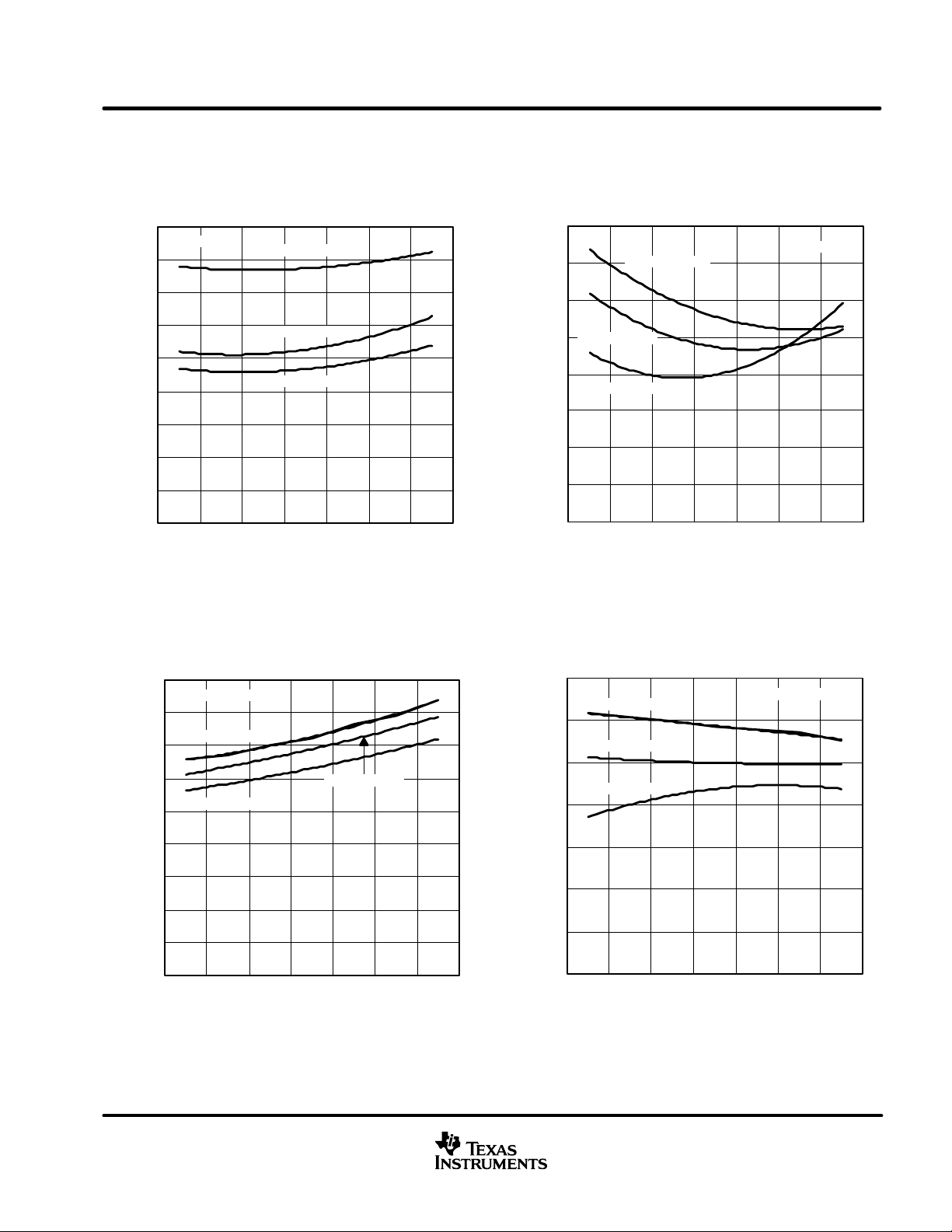
TYPICAL CHARACTERISTICS
SUPPLY CURRENT (RMS)
vs
FREQUENCY
33
32
31
30
29
28
– Supply Current (RMS) – mA
27
CC
I
26
25
0 250 500 750 1000 1250 1500 1750 2000
f – Frequency – kbps
Figure 9
BUS INPUT CURRENT
vs
BUS INPUT VOLTAGE
400
LOGIC INPUT CURRENT (D PIN)
vs
INPUT VOLTAGE
0
–2
–4
–6
–8
–10
– Logic Input Current – Aµ
–12
I(L)
I
–14
–16
0 0.6 1.1 1.6 2.1 2.6 3.1 3.6
VI – Input Voltage – V
Figure 10
DRIVER LOW-LEVEL OUTPUT CURRENT
vs
LOW-LEVEL OUTPUT VOLTAGE
180
300
Aµ
200
100
0
–100
– Bus Input Current –
I
I
–200
–300
–400
–7 –6 –4 –3 –10134678101112
VCC = 0 V
VCC = 3.6 V
VI – Bus Input Voltage – V
Figure 11
160
140
120
100
80
60
40
– Driver Low-Level Output Current – mA
20
OL
I
0
01234
V
O(CANL)
– Low-Level Output Voltage – V
Figure 12
www.ti.com
13

SN65HVD230Q-Q1
SN65HVD231Q-Q1
SN65HVD232Q-Q1
SGLS117C – JUNE 2001 – REVISED JUNE 2002
TYPICAL CHARACTERISTICS
– Driver High-Level Output Current – mA
OH
I
DRIVER HIGH-LEVEL OUTPUT CURRENT
vs
HIGH-LEVEL OUTPUT VOLTAGE
120
100
80
60
40
20
0
0 0.5 1 1.5 2 2.5 3 3.5
V
O(CANH)
– High-Level Output Voltage – V
Figure 13
– Dominant Voltage – V
V
OD
DOMINANT VOLTAGE (VOD)
vs
FREE-AIR TEMPERATURE
3
VCC = 3.6 V
2.5
VCC = 3.3 V
VCC = 3 V
2
1.5
1
0.5
0
–55 –40 0 25 70 85 125
TA – Free-Air Temperature – °C
Figure 14
RECEIVER LOW-TO-HIGH PROPAGATION DELAY TIME
vs
FREE-AIR TEMPERATURE
38
RS = 0
37
36
VCC = 3 V
VCC = 3.3 V
VCC = 3.6 V
TA – Free-Air Temperature – °C
– Receiver Low-to-High Propagation Delay Time – ns
PLH
t
35
34
33
32
31
30
–55 –40 0 25 70 85 125
Figure 15
RECEIVER HIGH-TO-LOW PROPAGATION DELAY TIME
vs
FREE-AIR TEMPERATURE
40
RS = 0
39
VCC = 3 V
VCC = 3.3 V
VCC = 3.6 V
TA – Free-Air Temperature – °C
– Receiver High-to-Low Propagation Delay Time – ns
PHL
t
38
37
36
35
34
–55 –40 0 25 70 85 125
Figure 16
14
www.ti.com
SN65HVD230Q-Q1
SN65HVD231Q-Q1
SN65HVD232Q-Q1
SGLS117C – JUNE 2001 – REVISED JUNE 2002
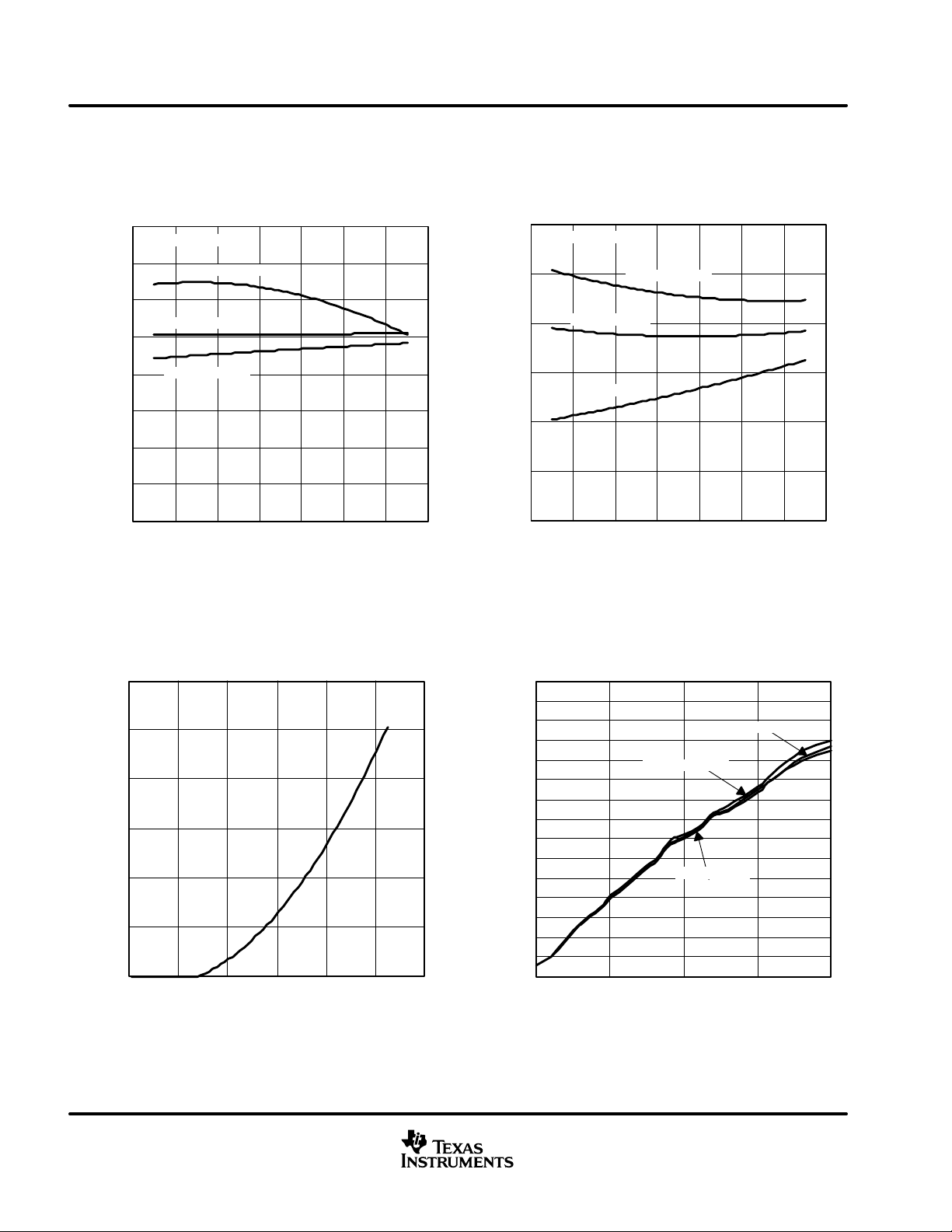
TYPICAL CHARACTERISTICS
DRIVER LOW-TO-HIGH PROPAGATION DELAY TIME
vs
FREE-AIR TEMPERATURE
55
– Driver Low-to-High Propagation Delay Time – ns
PLH
t
RS = 0
50
45
40
35
30
25
20
15
10
–55 –40 0 25 70 85 125
TA – Free-Air Temperature – °C
VCC = 3 V
VCC = 3.3 V
VCC = 3.6 V
Figure 17
DRIVER HIGH-TO-LOW PROPAGATION DELAY TIME
vs
FREE-AIR TEMPERATURE
90
RS = 0
– Driver High-to-Low Propagation Delay Time – ns
PHL
t
85
80
VCC = 3.3 V
75
70
65
60
55
50
–55 –40 0 25 70 85 125
VCC = 3.6 V
VCC = 3 V
TA – Free-Air Temperature – °C
Figure 18
DRIVER LOW-TO-HIGH PROPAGATION DELAY TIME
vs
FREE-AIR TEMPERATURE
90
RS = 10 kΩ
80
VCC = 3 V
70
VCC = 3.3 V
– Driver Low-to-High Propagation Delay Time – ns
PLH
t
60
VCC = 3.6 V
50
40
30
20
10
0
–55 –40 0 25 70 85 125
TA – Free-Air Temperature – °C
Figure 19
DRIVER HIGH-TO-LOW PROPAGATION DELAY TIME
vs
FREE-AIR TEMPERATURE
– Driver High-to-Low Propagation Delay Time – ns
PHL
t
150
VCC = 3.6 V
140
VCC = 3.3 V
130
VCC = 3 V
120
110
100
90
80
–55 –40 0 25 70 85 125
TA – Free-Air Temperature – °C
RS = 10 kΩ
Figure 20
www.ti.com
15
SN65HVD230Q-Q1
SN65HVD231Q-Q1
SN65HVD232Q-Q1
SGLS117C – JUNE 2001 – REVISED JUNE 2002
TYPICAL CHARACTERISTICS
DRIVER LOW-TO-HIGH PROPAGATION DELAY TIME
vs
FREE-AIR TEMPERATURE
800
RS = 100 kΩ
– Driver Low-to-High Propagation Delay Time – ns
PLH
t
700
600
500
400
300
200
100
0
–55 –40 0 25 70 85 125
VCC = 3 V
VCC = 3.3 V
VCC = 3.6 V
TA – Free-Air Temperature – °C
Figure 21
DRIVER HIGH-TO-LOW PROPAGATION DELAY TIME
vs
FREE-AIR TEMPERATURE
– Driver High-to-Low Propagation Delay Time – ns
PHL
t
1000
RS = 100 kΩ
950
900
850
800
750
700
VCC = 3.3 V
VCC = 3 V
–55 –40 0 25 70 85 125
VCC = 3.6 V
TA – Free-Air Temperature – °C
Figure 22
DRIVER OUTPUT CURRENT
vs
SUPPLY VOLTAGE
50
40
30
20
10
– Driver Output Current – mA
O
I
0
–10
1 1.5 2 2.5 3 3.5 4
VCC – Supply Voltage – V
Figure 23
DIFFERENTIAL DRIVER OUTPUT FALL TIME
vs
Source Resistance (RS)
1.50
1.40
1.30
1.20
1.10
1.00
0.90
0.80
0.70
0.60
0.50
0.40
0.30
– Differential Output Fall Time – sµ
0.20
f
t
0.10
0
0 50 100 150 200
Rs – Source Resistance – kΩ
VCC = 3.6 V
VCC = 3.3 V
VCC = 3 V
Figure 24
16
www.ti.com
SN65HVD230Q-Q1
SN65HVD231Q-Q1
SN65HVD232Q-Q1
SGLS117C – JUNE 2001 – REVISED JUNE 2002
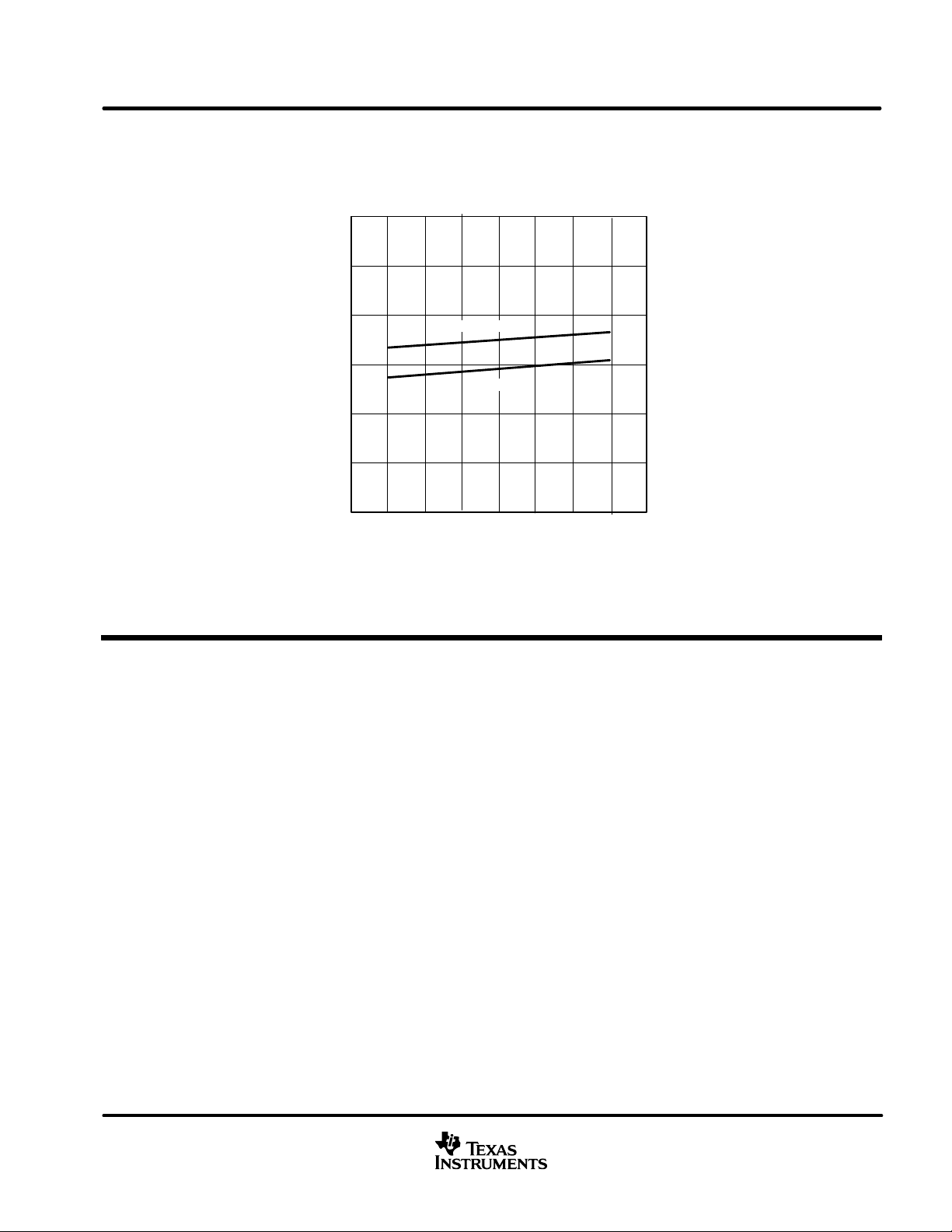
TYPICAL CHARACTERISTICS
REFERENCE VOLTAGE
vs
REFERENCE CURRENT
3
2.5
– Reference Voltage – V
ref
V
1.5
0.5
2
1
0
–50 –5550
VCC = 3.6 V
VCC = 3 V
I
– Reference Current – µA
ref
Figure 25
APPLICATION INFORMATION
This application provides information concerning the implementation of the physical medium attachment layer
in a CAN network according to the ISO 1 1898 standard. It presents a typical application circuit and test results,
as well as discussions on slope control, total loop delay, and interoperability in 5-V systems.
introduction
ISO 1 1898 is the international standard for high-speed serial communication using the controller area network
(CAN) bus protocol. It supports multimaster operation, real-time control, programmable data rates up to 1 Mbps,
and powerful redundant error checking procedures that provide reliable data transmission. It is suited for
networking intelligent devices as well as sensors and actuators within the rugged electrical environment of a
machine chassis or factory floor. The SN65HVD230Q family of 3.3-V CAN transceivers implement the lowest
layers of the ISO/OSI reference model. This is the interface with the physical signaling output of the CAN
controller of the Texas Instruments TMS320Lx240x 3.3-V DSPs, as illustrated in Figure 26.
www.ti.com
17
SN65HVD230Q-Q1
SN65HVD231Q-Q1
SN65HVD232Q-Q1
SGLS117C – JUNE 2001 – REVISED JUNE 2002
APPLICATION INFORMATION
Implementation
TMS320Lx2403/6/7
3.3-V
DSP
Embedded
CAN
Controller
SN65HVD230
CAN Bus–Line
Data-Link
Layer
Physical
Layer
ISO 11898 Specification
Application Specific Layer
Logic Link Control
Medium Access Control
Physical Signaling
Physical Medium Attachment
Medium Dependant Interface
Figure 26. The Layered ISO 11898 Standard Architecture
The SN65HVD230Q family of CAN transceivers are compatible with the ISO 11898 standard; this ensures
interoperability with other standard-compliant products.
application of the SN65HVD230Q
Figure 27 illustrates a typical application of the SN65HVD230Q family. The output of a DSP’s CAN controller
is connected to the serial driver input, pin D, and receiver serial output, pin R, of the transceiver. The transceiver
is then attached to the differential bus lines at pins CANH and CANL. T ypically , the bus is a twisted pair of wires
with a characteristic impedance of 120 Ω, in the standard half-duplex multipoint topology of Figure 28. Each end
of the bus is terminated with 120-Ω resistors in compliance with the standard to minimize signal reflections on
the bus.
18
www.ti.com

SN65HVD230Q-Q1
SN65HVD231Q-Q1
SN65HVD232Q-Q1
SGLS117C – JUNE 2001 – REVISED JUNE 2002
APPLICATION INFORMATION
Electronic Control Unit (ECU)
TMS320Lx2403/6/7
CAN-Controller
CANTX/IOPC6
DR
SN65HVD230
CANH CANL
CANRX/IOPC7
CAN Bus Line
Figure 27. Details of a Typical CAN Node
ECU ECU ECU
12 n
CANH
CAN Bus Line
CANL
120 Ω120 Ω
Figure 28. T ypical CAN Network
The SN65HVD230Q/231Q/232Q 3.3-V CAN transceivers provide the interface between the 3.3-V
TMS320Lx2403/6/7 CAN DSPs and the differential bus line, and are designed to transmit data at signaling rates
up to 1 Mbps as defined by the ISO 11898 standard.
features of the SN65HVD230Q, SN65HVD231Q, and SN65HVD232Q
The SN65HVD230Q/231Q/232Q are pin-compatible (but not functionally identical) with one another and,
depending upon the application, may be used with identical circuit boards.
These transceivers feature 3.3-V operation and standard compatibility with signaling rates up to 1 Mbps, and
also offer 16-kV HBM ESD protection on the bus pins, thermal shutdown protection, bus fault protection, and
open-circuit receiver failsafe. The failsafe design of the receiver assures a logic high at the receiver output if
the bus wires become open circuited. If a high ambient operating environment temperature or excessive output
current result in thermal shutdown, the bus pins become high impedance, while the D and R pins default to a
logic high.
www.ti.com
19
SN65HVD230Q-Q1
SN65HVD231Q-Q1
SN65HVD232Q-Q1
SGLS117C – JUNE 2001 – REVISED JUNE 2002
APPLICATION INFORMATION
features of the SN65HVD230Q, SN65HVD231Q, and SN65HVD232Q (continued)
The bus pins are also maintained in a high-impedance state during low VCC conditions to ensure glitch-free
power-up and power-down bus protection for hot-plugging applications. This high-impedance condition also
means that an unpowered node will not disturb the bus. Transceivers without this feature usually have a very
low output impedance. This results in a high current demand when the transceiver is unpowered, a condition
that could affect the entire bus.
operating modes
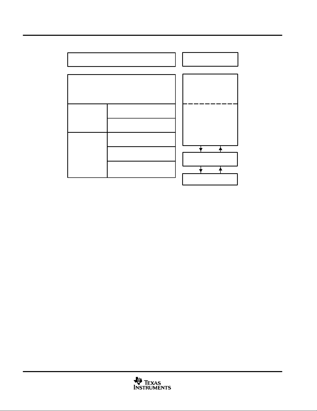
RS (pin 8) of the SN65HVD230Q and SN65HVD231Q provides for three different modes of operation:
high-speed mode, slope-control mode, and low-power standby mode.
high-speed mode
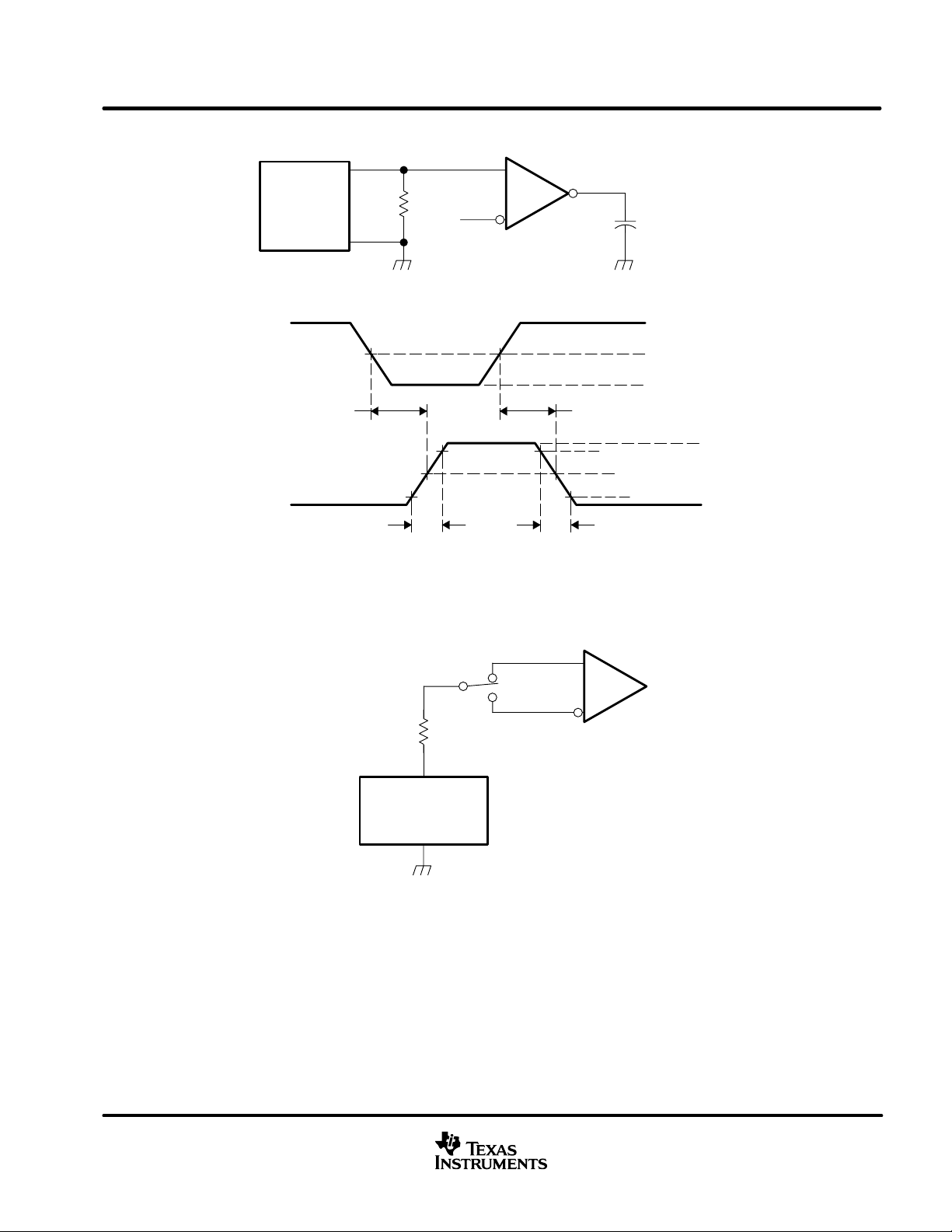
The high-speed mode can be selected by applying a logic low to Rs (pin 8). The high-speed mode of operation
is commonly employed in industrial applications. High-speed allows the output to switch as fast as possible with
no internal limitation on the output rise and fall slopes. The only limitations of the high-speed operation are cable
length and radiated emission concerns, each of which is addressed by the slope control mode of operation.
If the low-power standby mode is to be employed in the circuit, direct connection to a DSP output pin can be
used to switch between a logic-low level (< 1 V) for high speed mode operation, and the logic-high level (> 0.75
V
) for standby mode operation. Figure 29 shows a typical DSP connection, and Figure 30 shows the
CC
SN65HVD230Q driver output signal in high-speed mode on the CAN bus.
SN65HVD230Q
R
GND
V
CC
D
1
2
3
4
R
8
7
6
5
S
CANH
CANL
Vref
IOPF6
TMS320LF2406
or
TMS320LF2407
Figure 29. RS (Pin 8) Connection to a TMS320LF2406/07 for High-Speed or Standby Mode Operation
20
www.ti.com
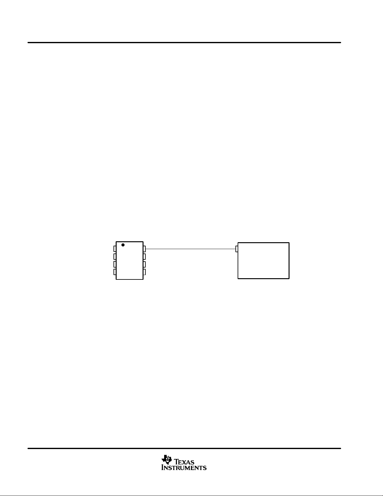
high-speed mode (continued)
1
SN65HVD230Q-Q1
SN65HVD231Q-Q1
SN65HVD232Q-Q1
SGLS117C – JUNE 2001 – REVISED JUNE 2002
APPLICATION INFORMATION
1 Mbps
Driver Output
NRZ Data
Figure 30. Typical SN65HVD230Q High-Speed Mode Output Waveform Into a 60-Ω Load
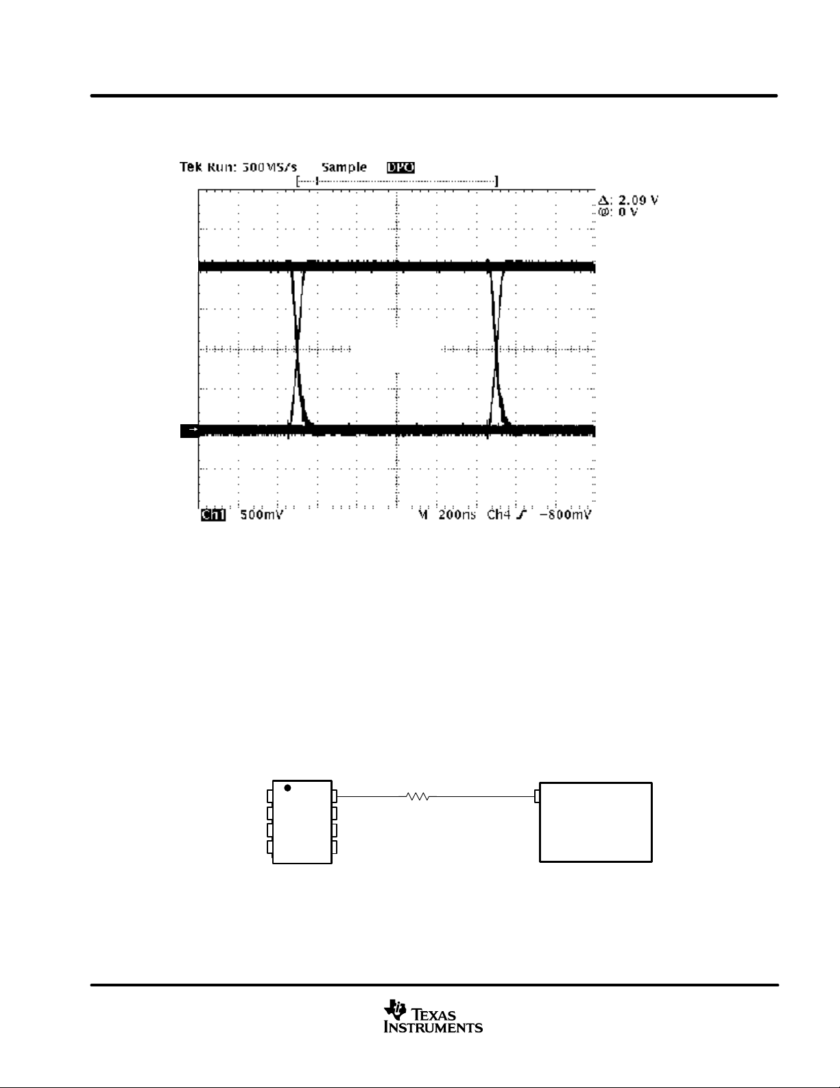
slope-control mode
Electromagnetic compatibility is essential in many applications using unshielded bus cable to reduce system
cost. T o reduce the electromagnetic interference generated by fast rise times and resulting harmonics, the rise
and fall slopes of the SN65HVD230Q and SN65HVD231Q driver outputs can be adjusted by connecting a
resistor from R
(pin 8) to ground or to a logic low voltage, as shown in Figure 31. The slope of the driver output
S
signal is proportional to the pin’s output current. This slope control is implemented with an external resistor value
of 10 kΩ to achieve a ≈ 15 V/µs slew rate, and up to 100 kΩ to achieve a ≈ 2.0 V/µs slew rate as displayed in
Figure 32. Typical driver output waveforms from a pulse input signal with and without slope control are displayed
in Figure 33. A pulse input is used rather than NRZ data to clearly display the actual slew rate.
SN65HVD230Q
D
GND
V
CC
R
R
1
2
3
4
8
7
6
5
S
CANH
CANL
Vref
10 kΩ
to
100 kΩ
IOPF6
TMS320LF2406
or
TMS320LF2407
Figure 31. Slope-Control or Standby Mode Connection to a DSP
www.ti.com
21

SN65HVD230Q-Q1
SN65HVD231Q-Q1
SN65HVD232Q-Q1
SGLS117C – JUNE 2001 – REVISED JUNE 2002
25
20
15
10
5
Driver Output Signal Slope – V/µs
APPLICATION INFORMATION
DRIVER OUTPUT SIGNAL SLOPE
vs
SLOPE CONTROL RESISTANCE
0
0 102030405060708090
4.70 6.8 10 15 22 33 47 68 100
Slope Control Resistance – kΩ
Figure 32. SN65HVD230Q Driver Output Signal Slope vs Slope Control Resistance Value
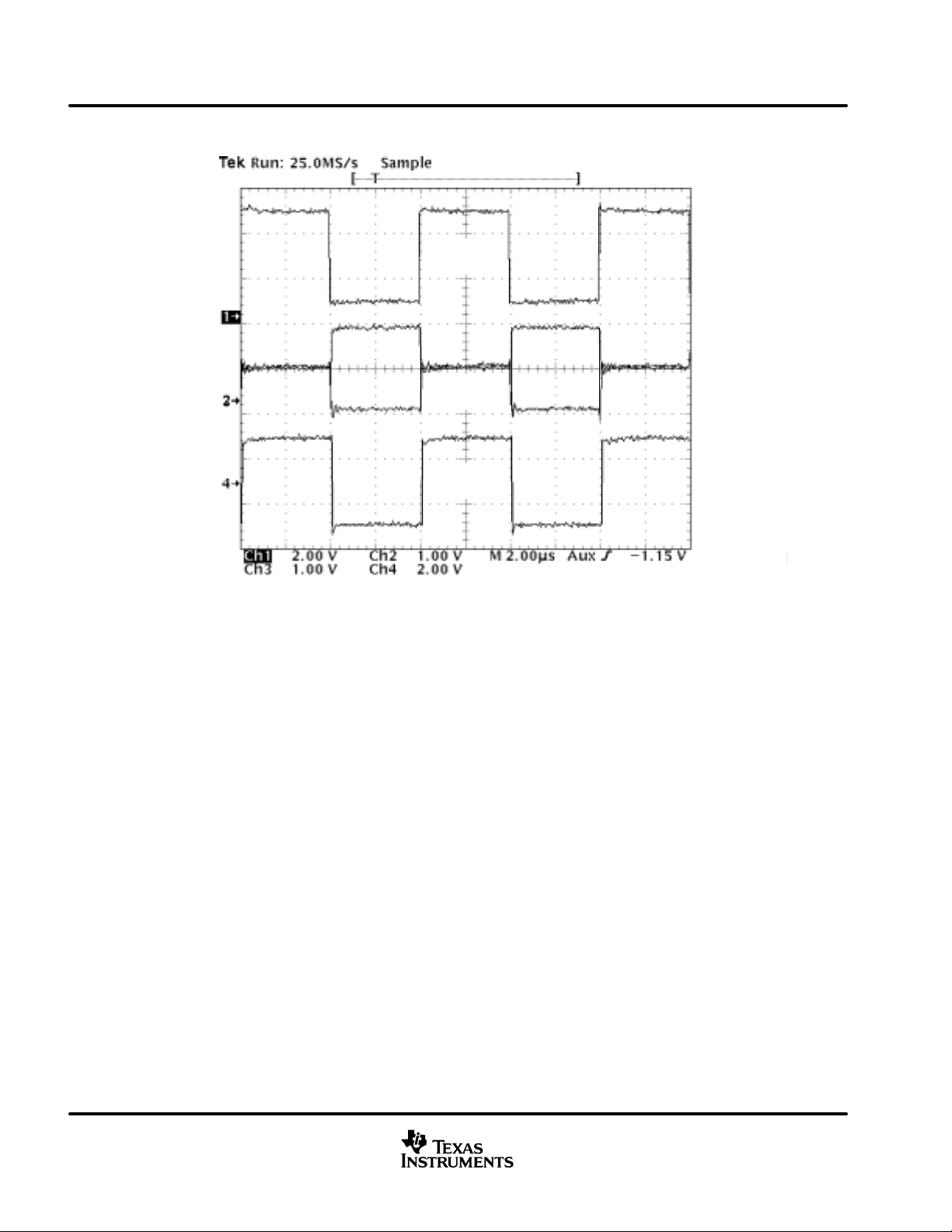
RS = 0 Ω
RS = 10 kΩ
RS = 100 kΩ
22
Figure 33. Typical SN65HVD230Q 250-kbps Output Pulse Waveforms With Slope Control
www.ti.com

APPLICATION INFORMATION
standby mode (listen only mode) of the SN65HVD230Q
SN65HVD230Q-Q1
SN65HVD231Q-Q1
SN65HVD232Q-Q1
SGLS117C – JUNE 2001 – REVISED JUNE 2002
If a logic high (> 0.75 V
a low-current, listen only standby mode during which the driver is switched off and the receiver remains active.
In this listen only state, the transceiver is completely passive to the bus. It makes no difference if a slope control
resistor is in place as shown in Figure 31. The DSP can reverse this low-power standby mode when the rising
edge of a dominant state (bus differential voltage > 900 mV typical) occurs on the bus. The DSP, sensing bus
activity, reactivates the driver circuit by placing a logic low (< 1.2 V) on R
the babbling idiot protection of the SN65HVD231Q
Occasionally, a runaway CAN controller unintentionally sends messages that completely tie up the bus (what
is referred to in CAN jargon as a babbling idiot). When this occurs, the DSP can engage the listen-only standby
mode to disengage the driver and release the bus, even when access to the CAN controller has been lost. When
the driver circuit is deactivated, its outputs default to a high-impedance state.
sleep mode of the SN65HVD231Q
The unique difference between the SN65HVD230Q and the SN65HVD231Q is that both driver and receiver are
switched off in the SN65HVD231Q when a logic high is applied to R
power-sleep mode until the circuit is reactivated with a logic low applied to R
the bus pins are in a high-impedance state, while the D and R pins default to a logic high.
) is applied to RS (pin 8) in Figures 29 and 31, the circuit of the SN65HVD230Q enters
CC
(pin 8).
S
(pin 8). The device remains in a very low
S
(pin 8). While in this sleep mode,
S
loop propagation delay
Transceiver loop delay is a measure of the overall device propagation delay, consisting of the delay from the
driver input to the differential outputs, plus the delay from the receiver inputs to its output.
The loop delay of the transceiver displayed in Figure 34 increases accordingly when slope control is being used.
This increased loop delay means that the total bus length must be reduced to meet the CAN bit-timing
requirements of the overall system. The loop delay becomes ≈100 ns when employing slope control with a
10-kΩ resistor, and ≈500 ns with a 100-kΩ resistor. Therefore, considering that the rule-of-thumb propagation
delay of typical bus cable is 5 ns/m, slope control with the 100-kΩ resistor decreases the allowable bus length
by the difference between the 500-ns max loop delay and the loop delay with no slope control, 70.7 ns. This
equates to (500–70.7 ns)/5 ns, or approximately 86 m less bus length. This slew-rate/bus length trade-off to
reduce electromagnetic interference to adjoining circuits from the bus can also be solved with a high-quality
shielded bus cable.
www.ti.com
23

SN65HVD230Q-Q1
SN65HVD231Q-Q1
SN65HVD232Q-Q1
SGLS117C – JUNE 2001 – REVISED JUNE 2002
APPLICATION INFORMATION
Figure 34. 70.7-ns Loop Delay Through the SN65HVD230Q With RS = 0
24
www.ti.com

SN65HVD230Q-Q1
SN65HVD231Q-Q1
SN65HVD232Q-Q1
SGLS117C – JUNE 2001 – REVISED JUNE 2002
APPLICATION INFORMATION
interoperability with 5-V CAN systems
It is essential that the 3.3-V SN65HVD230Q family performs seamlessly with 5-V transceivers because of the
large number of 5-V devices installed. Figure 35 displays a test bus of a 3.3-V node with the SN65HVD230Q,
and three 5-V nodes: one for each of TI’s SN65LBC031 and UC5350 transceivers, and one using a competitor
X250 transceiver.
Tektronix
784D
Tektronix
HFS–9003
Pattern
Generator
Trigger
Tektronix
P6243
Single-Ended
Probes
One Meter Belden Cable #82841
Input
Oscilloscope
120 Ω120 Ω
SN65HVD230Q
HP E3516A
3.3-V Power
Supply
SN65LBC031 UC5350
Figure 35. 3.3-V/5-V CAN Transceiver Test Bed
Competitor X250
HP E3516A
5-V Power
Supply
www.ti.com
25
SN65HVD230Q-Q1
SN65HVD231Q-Q1
SN65HVD232Q-Q1
SGLS117C – JUNE 2001 – REVISED JUNE 2002
APPLICATION INFORMATION
Driver
Input
CAN
Bus
Receiver
Output
Figure 36. SN65HVD230Q’s Input, CAN Bus, and X250’s RXD Output Waveforms
Figure 36 displays the SN65HVD230Q’s input signal, the CAN bus, and the competitor X250’s receiver output
waveforms. The input waveform from the Tektronix HFS-9003 Pattern Generator in Figure 35 to the
SN65HVD230Q is a 250-kbps pulse for this test. The circuit is monitored with Tektronix P6243, 1-GHz
single-ended probes in order to display the CAN dominant and recessive bus states.
Figure 36 displays the 250-kbps pulse input waveform to the SN65HVD230Q on channel 1. Channels 2 and
3 display CANH and CANL respectively , with their recessive bus states overlaying each other to clearly display
the dominant and recessive CAN bus states. Channel 4 is the receiver output waveform of the competitor X250.
26
www.ti.com
SN65HVD230Q-Q1
SN65HVD231Q-Q1
SN65HVD232Q-Q1
SGLS117C – JUNE 2001 – REVISED JUNE 2002
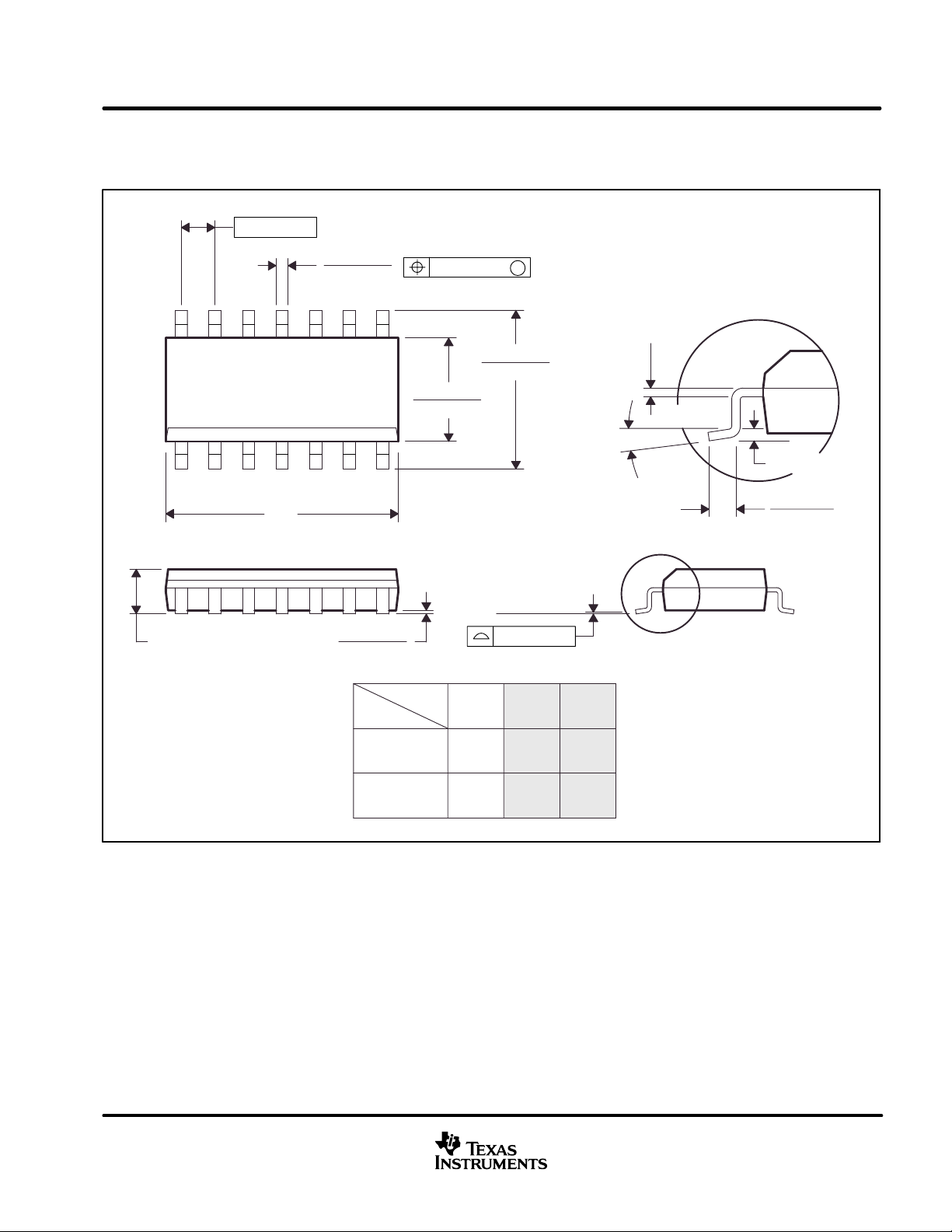
MECHANICAL DATA
D (R-PDSO-G**) PLASTIC SMALL-OUTLINE PACKAGE
14 PINS SHOWN
0.050 (1,27)
14
1
0.069 (1,75) MAX
0.020 (0,51)
0.014 (0,35)
8
7
A
0.010 (0,25)
0.004 (0,10)
DIM
0.157 (4,00)
0.150 (3,81)
PINS **
0.010 (0,25)
0.244 (6,20)
0.228 (5,80)
8
M
Seating Plane
0.004 (0,10)
14
0.008 (0,20) NOM
0°–ā8°
16
Gage Plane
0.010 (0,25)
0.044 (1,12)
0.016 (0,40)
A MAX
A MIN
NOTES: A. All linear dimensions are in inches (millimeters).
B. This drawing is subject to change without notice.
C. Body dimensions do not include mold flash or protrusion, not to exceed 0.006 (0,15).
D. Falls within JEDEC MS-012
0.197
(5,00)
0.189
(4,80)
www.ti.com
0.344
(8,75)
0.337
(8,55)
0.394
(10,00)
0.386
(9,80)
4040047/D 10/96
27

IMPORTANT NOTICE
Texas Instruments Incorporated and its subsidiaries (TI) reserve the right to make corrections, modifications,
enhancements, improvements, and other changes to its products and services at any time and to discontinue
any product or service without notice. Customers should obtain the latest relevant information before placing
orders and should verify that such information is current and complete. All products are sold subject to TI’s terms
and conditions of sale supplied at the time of order acknowledgment.
TI warrants performance of its hardware products to the specifications applicable at the time of sale in
accordance with TI’s standard warranty . Testing and other quality control techniques are used to the extent TI
deems necessary to support this warranty . Except where mandated by government requirements, testing of all
parameters of each product is not necessarily performed.
TI assumes no liability for applications assistance or customer product design. Customers are responsible for
their products and applications using TI components. T o minimize the risks associated with customer products
and applications, customers should provide adequate design and operating safeguards.
TI does not warrant or represent that any license, either express or implied, is granted under any TI patent right,
copyright, mask work right, or other TI intellectual property right relating to any combination, machine, or process
in which TI products or services are used. Information published by TI regarding third–party products or services
does not constitute a license from TI to use such products or services or a warranty or endorsement thereof.
Use of such information may require a license from a third party under the patents or other intellectual property
of the third party , or a license from TI under the patents or other intellectual property of TI.
Reproduction of information in TI data books or data sheets is permissible only if reproduction is without
alteration and is accompanied by all associated warranties, conditions, limitations, and notices. Reproduction
of this information with alteration is an unfair and deceptive business practice. TI is not responsible or liable for
such altered documentation.
Resale of TI products or services with statements different from or beyond the parameters stated by TI for that
product or service voids all express and any implied warranties for the associated TI product or service and
is an unfair and deceptive business practice. TI is not responsible or liable for any such statements.
Mailing Address:
Texas Instruments
Post Office Box 655303
Dallas, Texas 75265
Copyright 2002, Texas Instruments Incorporated

Copyright © Each Manufacturing Company.
All Datasheets cannot be modified without permission.
This datasheet has been download from :
www.AllDataSheet.com
100% Free DataSheet Search Site.
Free Download.
No Register.
Fast Search System.
www.AllDataSheet.com
 Loading...