

www.ti.com
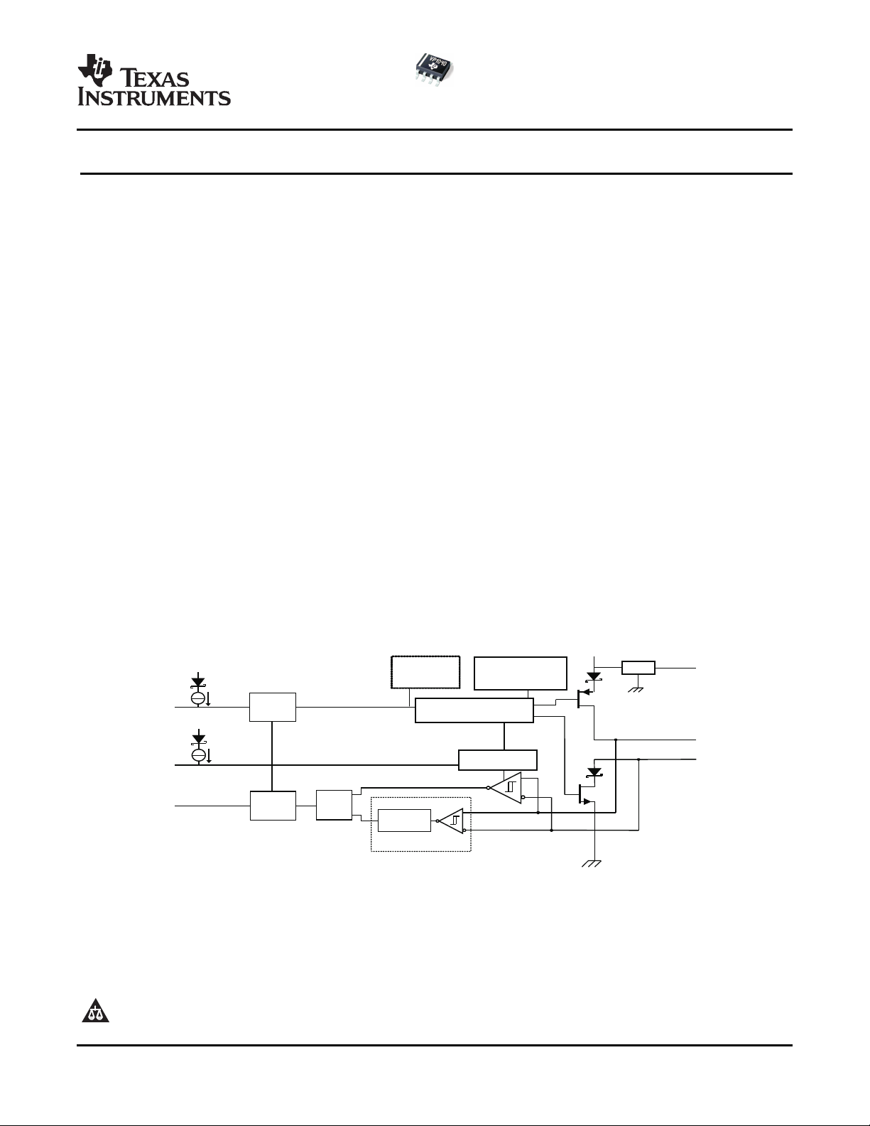
3
V
CC
CANH
7
6
CANL
4
RXD
WAKEUP
FILTER
BUSMONITOR
MUX
OVER
TEMPERATURE
SENSOR
DRIVER
TIME -OUT
DOMINANT
1
TXD
30 Am
STB
8
10 Am
SLEEP MODE
5
SPLIT
/ 2
2
OUTPUT
LOGIC
INPUT
LOGIC
V
CC
V
CC
V
CC
SN65HVD1040
SLLS631B – MARCH 2007 – REVISED APRIL 2007
LOW-POWER CAN TRANSCEIVER WITH BUS WAKE-UP
FEATURES APPLICATIONS
• Improved Drop-in Replacement for the
TJA1040
• ± 12 kV ESD Protection
• Low-Current Standby Mode with Bus
Wake-up: 5 µ A Typical
• Bus-Fault Protection of –27 V to 40 V
• Rugged Split-Pin Bus Stability
• Dominant Time-Out Function
• Power-Up/Down Glitch-Free Bus Inputs and
Outputs
– High Input Impedance with Low V
CC
– Monotonic Outputs During Power Cycling
• DeviceNet Vendor ID # 806
DESCRIPTION
The SN65HVD1040 meets or exceeds the specifications of the ISO 11898 standard for use in applications
employing a Controller Area Network (CAN). As CAN transceivers, these devices provide differential transmit
and receive capability for a CAN controller at signaling rates of up to 1 megabit per second (Mbps).
Designed for operation in especially harsh environments, the device features ± 12 kV ESD protection on the bus
and split pins, cross-wire, overvoltage and loss of ground protection from –27 to 40 V, overtemperature
shutdown, a –12 V to 12 V common-mode range, and will withstand voltage transients from –200 V to 200 V
according to ISO 7637.
• Battery Operated Applications
• Hand-Held Diagnostics
• Medical Scanning and Imaging
• HVAC
• Security Systems
• Telecom Base Station Status and Control
• SAE J1939 Standard Data Bus Interface
• NMEA 2000 Standard Data Bus Interface
• ISO 11783 Standard Data Bus Interface
• Industrial Automation
– DeviceNet™ Data Buses
(1)
(1) The signaling rate of a line is the number of voltage transitions that are made per second expressed in the units bps (bits per second).
Please be aware that an important notice concerning availability, standard warranty, and use in critical applications of Texas
Instruments semiconductor products and disclaimers thereto appears at the end of this data sheet.
DeviceNet is a trademark of Texas Instruments.
PRODUCTION DATA information is current as of publication date.
Products conform to specifications per the terms of the Texas
Instruments standard warranty. Production processing does not
necessarily include testing of all parameters.
Copyright © 2007, Texas Instruments Incorporated
www.ti.com
1
2
3
4
8
7
6
5
TXD
GND
V
CC
RXD
STB
CANH
CANL
SPLIT
SN65HVD1040
SN65HVD1040
SLLS631B – MARCH 2007 – REVISED APRIL 2007
These devices have limited built-in ESD protection. The leads should be shorted together or the device placed in conductive foam
during storage or handling to prevent electrostatic damage to the MOS gates.
DESCRIPTION (Continued)
The STB input (pin 8) selects between two different modes of operation; high-speed or low-power mode. The
high-speed mode of operation is selected by connecting STB to ground.
If a high logic level is applied to the STB pin of the SN65HVD1040, the device enters a low-power bus-monitor
standby mode. While the SN65HVD1040 is in the low-power bus-monitor standby mode, a dominant bit greater
than 5 µ s on the bus is passed by the bus-monitor circuit to the receiver output. The local protocol controller
may then reactivate the device when it needs to transmit to the bus.
A dominant-time-out circuit in the SN65HVD1040 prevents the driver from blocking network communication
during a hardware or software failure. The time-out circuit is triggered by a falling edge on TXD (pin 1). If no
rising edge is seen before the time-out constant of the circuit expires, the driver is disabled. The circuit is then
reset by the next rising edge on TXD.
The SPLIT output (pin 5) is available on the SN65HVD1040 as a V
split-termination network.
The SN65HVD1040 is characterized for operation from –40 ° C to 125 ° C.
/2 common-mode bus voltage bias for a
CC
ORDERING INFORMATION
PART NUMBER PACKAGE
SN65HVD1040 YES YES SOIC-8 VP1040
(1) For the most current package and ordering information, see the Package Option Addendum at the end of this document, or see the TI
website at www.ti.com .
DOMINANT LOW-POWER MARKED
TIME-OUT BUS MONITOR AS
(1)
ORDERING NUMBER
SN65HVD1040D (rail)
SN65HVD1040DR (reel)
2
Submit Documentation Feedback
www.ti.com
SN65HVD1040
SLLS631B – MARCH 2007 – REVISED APRIL 2007
ABSOLUTE MAXIMUM RATINGS
V
CC
V
I(bus)
I
O(OUT)
Supply voltage
Voltage range at any bus terminal (CANH, CANL, SPLIT) –27 V to 40 V
Receiver output current -20 mA to 20 mA
Voltage input, transient pulse
Human Body Model Bus terminals and GND ± 12 kV
ESD
Human body model
Charged-device-model
Machine model ± 200 V
V
I
T
J
Voltage input range (TXD, STB) –0.5 V to 6 V
Junction temperature –55 ° C to 170 ° C
(1) Stresses beyond those listed under "absolute maximum ratings" may cause permanent damage to the device. These are stress ratings
only and functional operation of the device at these or any other conditions beyond those indicated under "recommended operating
conditions" is not implied. Exposure to absolute-maximum-rated conditions for extended periods may affect device reliability.
(2) All voltage values, except differential I/O bus voltages, are with respect to network ground terminal.
(3) Tested in accordance with ISO 7637, test pulses 1, 2, 3a, 3b, 5, 6 & 7.
(4) Tested in accordance JEDEC Standard 22, Test Method A114-A.
(5) Tested in accordance JEDEC Standard 22, Test Method C101.
(2)
(4)
RECOMMENDED OPERATING CONDITIONS
V
CC
VIor V
V
IH
V
IL
V
ID
I
OH
I
OL
t
SS
T
J
(1) The algebraic convention, in which the least positive (most negative) limit is designated as minimum is used in this data sheet.
Supply voltage 4.75 5.25 V
Voltage at any bus terminal (separately or common mode) –12
IC
High-level input voltage 2 5.25 V
Low-level input voltage 0 0.8 V
Differential input voltage –6 6 V
High-level output current mA
Low-level output current mA
Maximum pulse width to remain in standby 0.7 µ s
Junction temperature –40 150 C
(1)
VALUE
–0.3 V to 7 V
(3)
, (CANH, CANL, SPLIT) –200 V to 200 V
All pins ± 4 kV
(5)
All pins ± 1 kV
MIN NOM MAX UNIT
(1)
TXD, STB
Driver –70
Receiver –2
Driver 70
Receiver 2
12 V
SUPPLY CURRRENT
over operating free-air temperature range (unless otherwise noted)
PARAMETER TEST CONDITIONS MIN TYP MAX UNIT
Dominant VI= 0 V, 60 Ω Load, STB at 0 V 50 70
I
CC
Supply current, V
CC
Recessive VI= VCC, STB at 0 V 6 10
Standby STB at VCC, VI = VCC 5 12 µ A
DEVICE SWITCHING CHARACTERISTICS
over recommended operating conditiions (unless otherwise noted)
PARAMETER
t
Total loop delay, driver input to receiver output, Recessive to Dominant 90 230
loop1
t
Total loop delay, driver input to receiver output, Dominant to Recessive 90 230
loop2
Submit Documentation Feedback
TEST MIN TYP MAX UNIT
CONDITIONS
STB at 0 V,
See Figure 9
mA
ns
3
www.ti.com
SN65HVD1040
SLLS631B – MARCH 2007 – REVISED APRIL 2007
DRIVER ELECTRICAL CHARACTERISTICS
over recommended operating conditiions (unless otherwise noted)
PARAMETER TEST CONDITIONS MIN TYP
V
O(D)
V
O(R)
V
O
V
OD(D)
V
SYM
V
OD(R)
V
OC(D)
V
OC(pp)
I
IH
I
IL
I
O(off)
I
OS(ss)
C
O
Bus output voltage VI= 0 V, STB at 0 V, RL= 60 Ω , See Figure 1 and
(Dominant) Figure 2
Bus output voltage (Recessive) VI= 3 V, STB at 0 V, See Figure 1 and Figure 2 2 2.5 3 V
Bus output voltage (Standby) RL= 60 Ω , STB at VCC, See Figure 1 and Figure 2 –0.1 0.1 V
Differential output voltage (Dominant) V
Output symmetry (Dominant or
Recessive) [ V
+ V
O(CANH)
Differential output voltage (Recessive) V
Common-mode output voltage
(Dominant)
Peak-to-peak common-mode output
voltage
High-level input current, TXD input VIat V
Low-level input current, TXD input VIat 0 V –50 –10 µ A
Power-off TXD Leakage current V
Short-circuit steady-state output
current
Output capacitance
(1) All typical values are at 25 C with a 5-V supply.
CANH 2.9 3.4 4.5
CANL 0.8 1.75
VI= 0 V, RL= 60 Ω , STB at 0 V, See Figure 1 and
Figure 2 , and Figure 3
VI= 0 V, RL= 45 Ω , STB at 0 V, See Figure 1 and
Figure 2
STB at 0 V, See Figure 2 and Figure 13 0.9 × V
)
O(CANL)
VI= 3 V, RL= 60 Ω , STB at 0 V, See Figure 1 and
Figure 2
VI= 3 V, STB at 0 V, No Load –0.5 0.05
STB at 0 V, See Figure 8 V
at 0 V, TXD at 5 V 1 µ A
CC
V
CANH
V
CANH
V
CANL
V
CANL
See Input capacitance to ground in RECEIVER
ELECTRICAL CHARACTERISTICS .
(1)
1.5 3
1.4 3
V
CC
1.1 × V
CC
–0.012 0.012
2 2.3 3
0.3
CC
–2 2 µ A
= –12 V, CANL Open, See Figure 12 –120 –72
= 12 V, CANL Open, See Figure 12 0.36 1
= –12 V, CANH Open, See Figure 12 –1 –0.5
= 12 V, CANH Open, See Figure 12 71 120
MAX UNIT
V
V
CC
mA
DRIVER SWITCHING CHARACTERISTICS
over recommended operating conditions (unless otherwise noted)
PARAMETER TEST CONDITIONS MIN TYP MAX UNIT
t
PLH
t
PHL
t
sk(p)
t
r
t
f
t
en
t
dom
4
Propagation delay time, low-to-high-level output 25 65 120
Propagation delay time, high-to-low-level output 25 45 120
Pulse skew (|t
– t
PHL
|) STB at 0 V, See Figure 4 25 ns
PLH
Differential output signal rise time 25
Differential output signal fall time 50
Enable time from silent mode to dominant See Figure 7 10 µ s
Dominant time-out See Figure 10 300 450 700 µ s
Submit Documentation Feedback
www.ti.com
RECEIVER ELECTRICAL CHARACTERISTICS
over recommended operating conditions (unless otherwise noted)
PARAMETER TEST CONDITIONS MIN TYP
Positive-going input threshold
V
IT+
voltage
Negative-going input threshold
V
IT–
voltage
V
Hysteresis voltage (V
hys
V
Input threshold voltage Standby mode STB at V
IT
V
High-level output voltage IO= –2 mA, See Figure 6 4 4.6 V
OH
V
Low-level output voltage IO= 2 mA, See Figure 6 0.2 0.4 V
OL
I
Power-off bus input current 5 µ A
I(off)
I
Power-off RXD leakage current V
O(off)
C
Input capacitance to ground, (CANH or CANL) TXD at 3 V, VI= 0.4 sin (4E6 π t) + 2.5 V 20 pF
I
C
Differential input capacitance TXD at 3 V, VI= 0.4 sin (4E6 π t) 10 pF
ID
R
Differential input resistance TXD at 3 V, STD at 0 V 30 80
ID
R
Input resistance, (CANH or CANL) TXD at 3 V, STD at 0 V 15 30 40
IN
Input resistance matching
R
I(m)
[1 – (R
IN (CANH)
/ R
– V
IT+
)] x 100%
IN (CANL)
(1) All typical values are at 25 C with a 5-V supply.
High-speed
mode 500 650
) STB at V
IT–
SN65HVD1040
SLLS631B – MARCH 2007 – REVISED APRIL 2007
(1)
800 900
STB at 0 V, See Table 1
CC
CC
CANH or CANL = 5 V, V
TXD at 0 V
at 0 V, RXD at 5 V 20 µ A
CC
V
= V
CANH
CANL
at 0 V,
CC
100 125
500 1150
–3% 0% 3%
MAX UNIT
mV
k Ω
RECEIVER SWITCHING CHARACTERISTICS
over recommended operating conditiions (unless otherwise noted)
PARAMETER TEST CONDITIONS MIN TYP MAX UNIT
t
Propagation delay time, low-to-high-level output 60 100 130
pLH
t
Propagation delay time, high-to-low-level output 45 70 130
pHL
t
Output signal rise time 8
r
t
Output signal fall time 8
f
t
Dominant time required on bus for wake-up from
BUS
(1)
standby
(1) The device under test shall not signal a wake-up condition with dominant pulses shorter than t
condition with dominant pulses longer than t
wake-up.
(max). Dominant pulses with a length between t
BUS
STB at 0 V, TXD at 3 V, See
Figure 6
STB at V
Figure 11 0.7 5 µ s
CC
(min) and shall signal a wake-up
BUS
(min) and t
BUS
BUS
SPLIT-PIN CHARACTERISTICS
over recommended operating conditiions (unless otherwise noted)
PARAMETER TEST CONDITIONS MIN TYP MAX UNIT
V
O
I
O(stb)
Output voltage –500 µ A < IO< 500 µ A 0.3 × V
0.5 × V
CC
CC
Standby mode leakage current STB at 2 V, –12 V ≤ VO≤ 12 V –5 5 µ A
STB-PIN CHARACTERISTICS
over recommended operating conditiions (unless otherwise noted)
PARAMETER TEST CONDITIONS MIN TYP MAX UNIT
I
High level input current STB at 2 V –10 0 µ A
IH
I
Low level input current STB at 0 V –10 0 µ A
IL
ns
(max) may lead to a
0.7 × V
V
CC
Submit Documentation Feedback
5
www.ti.com
2.5 V
3.5
V
1.5 V
Recessive
Dominant
O
(CANH)
V
O
(CANL)
V
TXD
STB
I
I
V
I
V
OD
R
L
2
I
O(CANH)
V
O(CANH)
V
OC
I
O(CANL)
V
O(CANL)
V
O(CANH)
+ V
O(CANL)
0 V
V
OD
+
_
CANH
CANL
TXD
STB
60 +1%
330 +1%
330 +1%
−2 V 3 V
TEST
3 7 V
RL = 60 W
+1‘%
V
O
STB
CANH
CANH
V
I
TXD
(see Note A)
t
f
t
r
10%
90%
0.9 V
0 V
V
O(D)
V
I
V
O
V
O(R)
CL = 100 pF +20%
(see Note B)
V
CC
2
V
CC
2
t
PLH
t
PHL
0.5 V
V
CC
V
O
CANH
CANL
RXD
V
I
(CANH)
V
I
(CANL)
I
O
V
ID
V
I(CANH)
+ V
I(CANL)
2
VIC =
SN65HVD1040
SLLS631B – MARCH 2007 – REVISED APRIL 2007
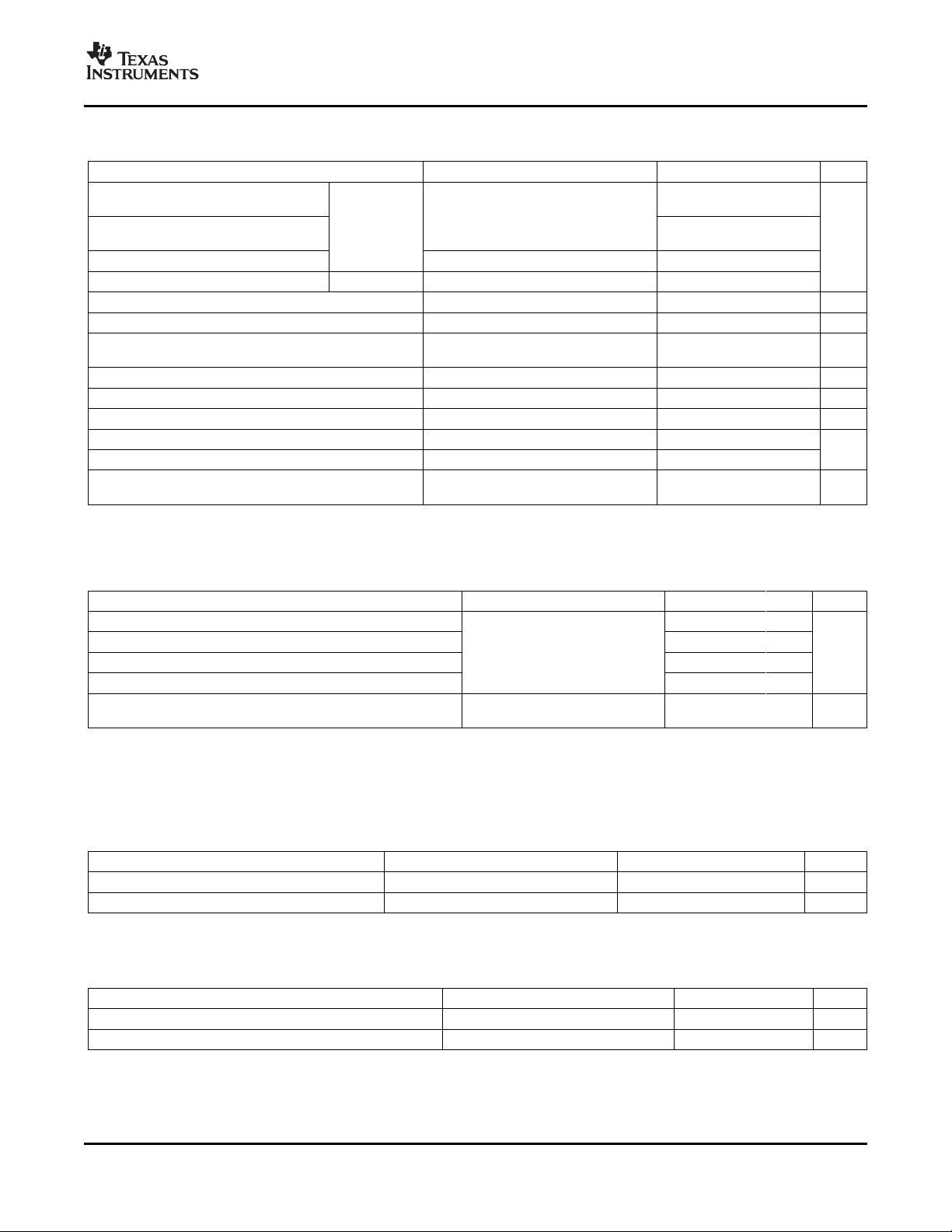
Figure 1. Driver Voltage, Current, and Test Definition Figure 2. Bus Logic State Voltage Definitions
PARAMETER MEASUREMENT INFORMATION
Figure 3. Driver V
Figure 4. Driver Test Circuit and Voltage Waveforms
Figure 5. Receiver Voltage and Current Definitions
Test Circuit
OD
6
Submit Documentation Feedback
www.ti.com
CANH
CANL
RXD
V
I
STB
V
O
I
O
2V
2.4V
3.5V
V
OH
t
f
t
r
1.5V
V
OL
90%
10%
V
I
V
O
1.5V
(seeNote A)
CL=15pF 20%
(seeNoteB)
t
PLH
t
PLH
0.7V
CC
0.3V
CC
50%
50%
CANH
CANL
C
L
TXD
STB
RXD
+
V
O
−
15 pF 20%
DUT
60 W 1%
V
I
V
O
t
en
V
CC
0 V
V
OH
V
OL
NOTE: CL = 100 pF
Includes Instrumentation
and Fixture Capacitance
Within ±20%
CANH
CANL
V
I
TXD
STB
27 W +1%
27 W +1%
47 nF
+20%
VOC =
V
O (CANH)
+ V
O (CANL)
2
V
OC
V
OC(PP)
SN65HVD1040
SLLS631B – MARCH 2007 – REVISED APRIL 2007
PARAMETER MEASUREMENT INFORMATION (continued)
A. The input pulse is supplied by a generator having the following characteristics: PRR ≤ 125 kHz, 50% duty cycle, tr≤
6 ns, tf≤ 6ns, ZO= 50 Ω .
B. CLincludes instrumentation and fixture capacitance within 20%.
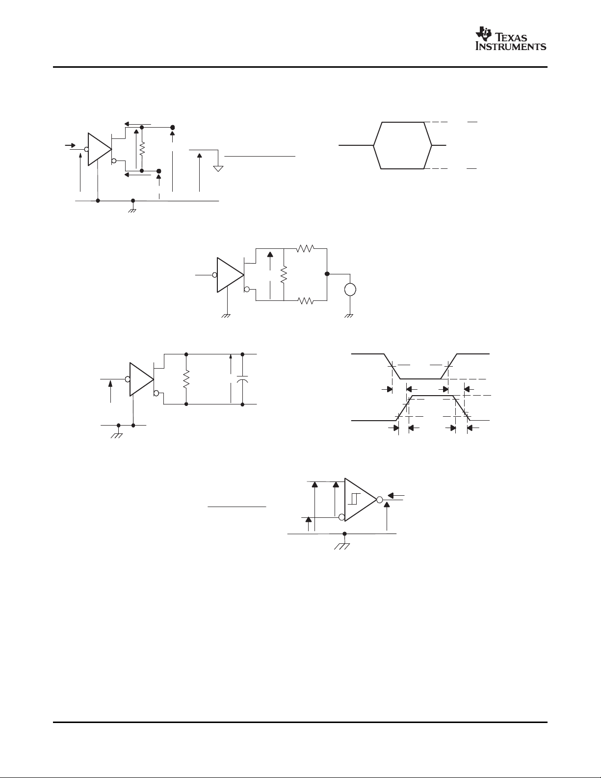
Figure 6. Receiver Test Circuit and Voltage Waveforms
Table 1. Differential Input Voltage Threshold Test
INPUT OUTPUT
V
CANH
–11.1 V –12 V 900 mV L V
12 V 11.1 V 900 mV L
–6 V –12 V 6 V L
12 V 6 V 6 V L
–11.5 V –12 V 500 mV H V
12 V 11.5 V 500 mV H
–12 V –6 V 6 V H
6 V 12 V 6 V H
Open Open X H
V
CANL
|V
| R
ID
OL
OH
Figure 7. tenTest Circuit and Voltage Waveforms
A. All VIinput pulses are from 0 V to V
Pulse Repetition Rate (PRR) = 125 kHz, 50% duty cycle.
Figure 8. Peak-to-Peak Common Mode Output Voltage Test and Waveform
and supplied by a generator having the following characteristics: tror tf≤ 6 ns.
CC
Submit Documentation Feedback
7

www.ti.com
50%
50%50%
NOTE: CL = 100 pF
Includes Instrumentation
and Fixture Capacitance
Within ±20%
CANH
CANL
C
L
TXD
STB
RXD
+
V
O
−
15 pF 20%
DUT
60 W 1%
TXD
Input
RXD Output
t
loop2
t
loop1
V
CC
0 V
V
OH
V
OL
STB
CANH
CANL
V
O
500 mV
900 mV
C
L
(see Note B)
RL = 60 W +1%
TXD
(see Note A)
V
I
V
O
t
dom
V
CC
0 V
V
OD(D)
0 V
V
I
1.5 V
CANH
CANL
RXD
V
O
V
I
I
O
C
L
STB
3.5 V
V
I
V
O
400 mV
2.65 V
1.5 V
V
OH
V
OL
(see Note A)
V
CC
(see Note B)
0.7 s
t
BUS
SN65HVD1040
SLLS631B – MARCH 2007 – REVISED APRIL 2007
A. All VIinput pulses are from 0 V to V
and supplied by a generator with the following characteristics: tror tf≤ 6 ns.
CC
Pulse Repetition Rate (PRR) = 125 kHz, 50% duty cycle.
Figure 9. t
A. All VIinput pulses are from 0 V to V
Test Circuit and Voltage Waveforms
loop
and supplied by a generator with the following characteristics: tror tf≤ 6 ns.
CC
Pulse Repetition Rate (PRR) = 500 Hz, 50% duty cycle.
B. CL= 100 pF includes instrumentation and fixture capacitance within 20%.
Figure 10. Dominant Time-Out Test Circuit and Waveform
8
A. For VIbit width ≤ 0.7 µ s, VO= VOH. For VII bit width ≥ 5 µ s, VO= VOL. VIinput pulses are supplied from a generator
with the following characteristics; tror tf≤ 6 ns. Pulse Repetition Rate (PRR) = 50 Hz, 30% duty cycle.
B. CL= 15 pF includes instrumentation and fixture capacitance within 20%.
Figure 11. t
Submit Documentation Feedback
Test Circuit and Waveform
BUS

www.ti.com
CANH
CANL
STB
V
in
V
in
0 V
0 V
12 V
−12 V
or
0 V
0 V or V
CC
TXD
I
OS
V
IN
−12 V or 12 V
I
OS(P)
200 ms
I
OS(SS)
10 ms
CANH
CANL
4.7 nF
V
I
TXD
STB
60 1%
60 1%
O(CANL)
V
O(CANH)
V
SYM
V
=
+
O
(CANL)
V
O
(CANH)
V
20%
±
W
W
±
±
Figure 12. Driver Short-Circuit Current Test and Waveform
SN65HVD1040
SLLS631B – MARCH 2007 – REVISED APRIL 2007
Figure 13. Driver Output Symmetry Test Circuit
Submit Documentation Feedback
9

www.ti.com
SN65HVD1040
SLLS631B – MARCH 2007 – REVISED APRIL 2007
DEVICE INFORMATION
Table 2. DRIVER FUNCTION TABLE
(1)
INPUTS OUTPUTS BUS STATE
TXD STB CANH CANL
L L H L DOMINANT
H L Z Z RECESSIVE
Open X Z Z RECESSIVE
X H or Open Z Z RECESSIVE
(1) H = high level; L = low level; X = irrelevant; Z = high impedance
Table 3. RECEIVER FUNCTION TABLE
(1)
DIFFERENTIAL INPUTS STB OUTPUT BUS STATE
VID= CANH - CANL RXD
VID≥ 0.9 V L L DOMINANT
VID≥ 1.15 V H or Open L DOMINANT
0.5 V < VID< 0.9 V X ? ?
VID≤ 0.5 V X H RECESSIVE
Open X H RECESSIVE
(1) H = high level; L = low level; X = irrelevant; ? = indeterminate; Z =
high impedance
THERMAL CHARACTERISTICS
over operating free-air temperature range (unless otherwise noted)
PARAMETER TEST CONDITIONS MIN TYP MAX UNIT
θ
Thermal Resistance, Junction-to-Air
JA
θ
Thermal Resistance, 53
JB
Junction-to-Board
θ
Thermal Resistance, 79
JC
Junction-to-Case
P
Device Power Dissipation 112 170 mW
D
T
Junction Temperature, Thermal Shutdown
JS
Low-K Thermal Resistance
High-K Thermal Resistance 131 ° C/W
RL= 60 Ω , S at 0 V,
Input to TXD a 500kHz 50% duty-cycle square wave
(2)
(1) Tested in accordance with the Low-K or High-K thermal metric definitions of EIA/JESD51-3 for leaded surface mount packages.
(2) Extended operation in thermal shutdown may affect device reliability, see the Application Information section.
(1)
211 ° C/W
° C/W
190 ° C
10
Submit Documentation Feedback

www.ti.com
V
V
I
I
V
V
V
V
V
V
I
I
R
R
R
C
C
I
I
V
t
t
t
t
t
t
V
V
I
I
IH
IL
IH
IL
th(dif)
hys(dif)
O(dom)
O(reces)
i(dif)(th)
O(dif0(bus)
LI
O(SC)
OH
OL
O
d(TXD-BUSon)
d(TXD-BUSoff)
d(BUSon-RXD)
d(BUSoff-RXD)
PD(TXD–RXD)
d(stb-norm)
IH
IL
IH
IL
SN65HVD1040
SLLS631B – MARCH 2007 – REVISED APRIL 2007
DEVICE INFORMATION
Table 4. Parametric Cross Reference With the TJA1040
TJA1040
i(cm)
i(def)
i(cm) (m)
i(cm)
i(dif)
(1)
PARAMETER HVD10xx
TJA1040 DRIVER SECTION
High-level input voltage Recommended V
Low-level input voltage Recommended V
High-level input current Driver I
Low-level input current Driver I
IH
IL
TJA1040 BUS SECTION
Differential input voltage Receiver VITand recommended V
Differential input hysteresis Receiver V
Dominant output voltage Driver V
Recessive output voltage Driver V
hys
O(D)
O(R)
Differential input voltage Receiver VITand recommended V
Differential bus voltage Driver V
Power-off bus input current Receiver I
Short-circuit output current Driver I
CANH, CANL input resistance Receiver R
Differential input resistance Receiver R
Input resistance matching Receiver R
Input capacitance to ground Receiver C
Differential input capacitance Receiver C
and V
OD(D)
I(off)
OS(SS)
IN
ID
I (m)
I
ID
TJA1040 RECEIVER SECTION
High-level output current Recommended I
Low-level output current Recommended I
OH
OL
TJA1040 SPLIT PIN SECTION
Reference output voltage V
O
TJA1040 TIMING SECTION
Delay TXD to bus active Driver t
Delay TXD to bus inactive Driver t
Delay bus active to RXD Receiver t
Delay bus inactive to RXD Receiver t
Prop delay TXD to RXD Device t
Enable time from standby to dominant Driver t
PLH
PHL
PHL
PLH
and t
LOOP1
en
TJA1040 STB PIN SECTION
High-level input voltage Recommended V
Low-level input voltage Recommended V
High-level input current I
Low-level input current I
IH
IL
IH
IL
ID
ID
OD(R)
LOOP2
IH
IL
(1) From TJA1040 Product Specification, Philips Semiconductors, 2003 February 19.
Submit Documentation Feedback
11

www.ti.com
Vcc
RXDOutput
6 V
Output
15
W
Vcc
SPLITOutput
Output
2 k W
2 k W
40 V
STBInput
Vcc
6 V
Input
W
Vcc
40 V
Output
CANHandCANL Outputs
CANHInput
Vcc
20 k
40 V
Input
10 k W
10 kW
W
TXDInput
Vcc
4. 3 k
6 V
Input
W
CANL Input
Vcc
20k
40 V
Input
10 k W
10 kW
W
4.3 k
SN65HVD1040
SLLS631B – MARCH 2007 – REVISED APRIL 2007
Equivalent Input and Output Schematic Diagrams
12
Submit Documentation Feedback

www.ti.com
120
125
130
135
140
145
150
−40 0 25 70 125
VCC=4.75V
VCC=5V
VCC=5.25V
−
Recessive-to-DominantLoopT
ime − ns
t
L
OOP1
TA− Free-AirTemperature −°C
Sat0V,
R =60 ,
C =100pF,
AirFlowat7cf/m,
TXDInputisa125kHz,
50%DutyCyclePulse
L
L
W
140
145
150
155
160
165
170
−40 0 25 70 125
VCC=5.25V
− Dominant-to-RecessiveLoopT
ime − ns
t
LOOP2
TA− Free-AirTemperature −°C
VCC=5V
VCC=4.75V
Sat0V,
R =60 ,
C =100pF,
AirFlowat7cf/m,
TXDInputisa125kHz,
50%DutyCyclePulse
L
L
W
−10
0
10
20
30
40
50
60
70
80
90
0 1 2 3 4 5
TA = 255C,
VCC = 5 V ,
S at 0 V ,
TXD Input is a 125 kHz
1% Duty Cycle Pulse
I
OL
− Low-Level Output Current − mA
VOCANL − Low-Level Output Voltage − V
0
5
10
15
20
25
30
35
40
45
50
200 400 500 600 800 1000
Signaling Rate − kbps
I
CC
− RMS Supply Current − mA
TA = 255C,
VCC = 5 V ,
S at 0 V ,
RL = 60 W,
RXD = 15 pF
SN65HVD1040
SLLS631B – MARCH 2007 – REVISED APRIL 2007
TYPICAL CHARACTERISTICS
RECESSIVE-TO-DOMINANT LOOP TIME DOMINANT-TO-RECESSIVE LOOP TIME
vs vs
FREE-AIR TEMPERATURE (across VCC) FREE-AIR TEMPERATURE (across VCC)
Figure 14. Figure 15.
SUPPLY CURRENT (RMS) DRIVER LOW-LEVEL OUTPUT VOLTAGE
vs vs
SIGNALING RATE LOW-LEVEL OUTPUT CURRENT
Figure 16. Figure 17.
Submit Documentation Feedback
13
www.ti.com
-0
-10
-20
-30
-40
-50
-60
-70
-80
0 1 2 3 4 5
TA=25 C,
V
CC
=5V,
Sat0V,
TXDInputisa125kHz
1%DutyCyclePulse
I
OH
− High-LevelOutputCurrent − mA
VOCANH − High-LevelOutputVoltage − V
0
0.5
1
1.5
2
2.5
3
−40 0 25 70 125
S at 0 V ,
RL = 60 W,
Air Flow at 7 cf/m,
TXD Input is a 125 kHz
1% Duty Cycle Pulse
TA − Free-Air Temperature − °C
VCC = 5 V
VCC = 4.75 V
VCC = 5.25 V
Dominant Driver Differential Output Voltage − V
0
5
10
15
20
25
30
35
40
45
50
1 2 3 3.5 4 4.5 5 5.25
TA = 255C,
VCC = 5 V ,
S at 0 V ,
RL = 60 W,
TXD Input is a 125 kHz
1% Duty Cycle Pulse
I
O
− Differential Driver Output Current − mA
VCC − Supply Voltage − V
−1
0
1
2
3
4
5
6
0.60
0.65
0.70
0.75
0.80
0.85
1
0.85
0.80
0.75
0.70
0.65
0.60
V
IT+
V
IT−
VCM = 12 V
VCM = 2.5 V
VCM = −12 V
TA = 255C,
VCC = 5 V ,
S at 0 V ,
RXD = 15 pF
− Receiver Output Voltage − V
V
O
VID − Differential Input Voltage − V
SN65HVD1040
SLLS631B – MARCH 2007 – REVISED APRIL 2007
TYPICAL CHARACTERISTICS (continued)
DRIVER HIGH-LEVEL OUTPUT VOLTAGE DRIVER DIFFERENTIAL OUTPUT VOLTAGE
vs vs
HIGH-LEVEL OUTPUT CURRENT FREE-AIR TEMPERATURE (across VCC)
Figure 18. Figure 19.
DRIVER OUTPUT CURRENT RECEIVER OUTPUT VOLTAGE
vs vs
SUPPLY VOLTAGE DIFFERENTIAL INPUT VOLTAGE
14
Figure 20. Figure 21.
Submit Documentation Feedback

www.ti.com
DB Vm
0
20
40
60
80
0.1 1 10 100 1000
f − Frequency − MHz
dBm
TYPICAL CHARACTERISTICS (continued)
TYPICAL ELECTROMAGNETIC EMISSIONS TYPICAL ELECTROMAGNETIC
UP TO 50 MHZ (Peak Amplitude) IMMUNITY PERFORMANCE
SN65HVD1040
SLLS631B – MARCH 2007 – REVISED APRIL 2007
Figure 22. Frequency Spectrum of Common-Mode Figure 23. Direct Power Injection (DPI) Response vs
Emissions Frequency
Submit Documentation Feedback
15

www.ti.com
SN65HVD1040
SLLS631B – MARCH 2007 – REVISED APRIL 2007
APPLICATION INFORMATION
CAN Basics
The basics of arbitration require that the receiver at the sending node designate the first bit as dominant or
recessive after the initial wave of the first bit of a message travels to the most remote node on a network and
back again. Typically, this “sample” is made at 75% of the bit width, and within this limitation, the maximum
allowable signal distortion in a CAN network is determined by network electrical parameters.
Factors to be considered in network design include the approximately 5 ns/m propagation delay of typical
twisted-pair bus cable; signal amplitude loss due to the loss mechanisms of the cable; and the number, length,
and spacing of drop-lines (stubs) on a network. Under strict analysis, variations among the different oscillators in
a system also need to be accounted for with adjustments in signaling rate and stub and bus length. Table 5 lists
the maximum signaling rates achieved with the SN65HVD1040 with several bus lengths of category 5, shielded
twisted pair (CAT 5 STP) cable.
Table 5. Maximum Signaling Rates for Various Cable
Lengths
Bus Length (m) Signaling Rate (kbps)
30 1000
100 500
250 250
500 125
1000 62.5
The ISO 11898 Standard specifies a maximum bus length of 40 m and maximum stub length of 0.3 m with a
maximum of 30 nodes. However, with careful design, users can have longer cables, longer stub lengths, and
many more nodes to a bus. (Note: Non-standard application may come with a trade-off in signaling rate.) A large
number of nodes requires a transceiver with high input impedance such as the HVD1040.
The Standard specifies the interconnect to be a single twisted-pair cable (shielded or unshielded) with 120 Ω
characteristic impedance (Z
). Resistors equal to the characteristic impedance of the line terminate both ends of
O
the cable to prevent signal reflections. Unterminated drop-lines connect nodes to the bus and should be kept as
short as possible to minimize signal reflections.
Connectors, while not specified by the standard should have as little effect as possible on standard operating
parameters such as capacitive loading. Although unshielded cable is used in many applications, data
transmission circuits employing CAN transceivers are usually used in applications requiring a rugged
interconnection with a wide common-mode voltage range. Therefore, shielded cable is recommended in these
electronically harsh environments, and when coupled with the Standard’s –2-V to 7-V common-mode range of
tolerable ground noise, helps to ensure data integrity. The HVD1040 enhances the Standard’s insurance of data
integrity with an extended –12 V to 12 V range of common-mode operation.
16
Submit Documentation Feedback

www.ti.com
75% SAMPLE POINT
500 mV Threshold
900 mV Threshold
ALLOWABLE JITTER
NOISE MARGIN
NOISE MARGIN
RECEIVER DETECTION WINDOW
W
120
W
120
CANH
CANL
TMS320LF243
SN65HVD1040
D R
STB
SPLIT
CANTX CANRX
Sensor, Actuator, or Control
Equipment
TMS320LF243
D R
0.1mF
Vcc
GND
STB
CANTX CANRX
Sensor, Actuator, or Control
Equipment
TMS320LF2407A
SN65HVD230
D R
Rs
Vref
CANTX CANRX
Sensor, Actuator, or Control
Equipment
5 V
0.1mF
Vcc
GND
5 V
0.1mF
Vcc
GND
3.3 V
Stub Lines -- 0.3m max
Bus Lines -- 40 mmax
SN65HVD1040
SPLIT
Figure 24. Typical CAN Differential Signal Eye-Pattern
SN65HVD1040
SLLS631B – MARCH 2007 – REVISED APRIL 2007
An eye pattern is a useful tool for measuring overall signal quality. As displayed in Figure 25 , the differential
signal changes logic states in two places on the display, producing an “eye.” Instead of viewing only one logic
crossing on the scope, an entire “bit” of data is brought into view. The resulting eye pattern includes all of the
effects of systemic and random distortion, and displays the time during which a signal may be considered valid.
The height of the eye above or below the receiver threshold voltage level at the sampling point is the noise
margin of the system. Jitter is typically measured at the differential voltage zero-crossing during the logic state
transition of a signal. Note that jitter present at the receiver threshold voltage level is considered by some to be a
more effective representation of the jitter at the input of a receiver.
As the sum of skew and noise increases, the eye closes and data is corrupted. Closing the width decreases the
time available for accurate sampling, and lowering the height enters the 900 mV or 500 mV threshold of a
receiver.
Different sources induce noise onto a signal. The more obvious noise sources are the components of a
transmission circuit themselves; the signal transmitter, traces and cables, connectors, and the receiver. Beyond
that, there is a termination dependency, cross-talk from clock traces and other proximity effects, V
and ground
CC
bounce, and electromagnetic interference from near-by electrical equipment.
The balanced receiver inputs of the HVD1040 mitigate most all sources of signal corruption, and when used with
a quality shielded twisted-pair cable, help insure data integrity.
Figure 25. Typical HVD1040 Application
Submit Documentation Feedback
17

www.ti.com
SN65HVD1040
SLLS631B – MARCH 2007 – REVISED APRIL 2007
Thermal Shutdown
The SN65HVD1040 has a thermal shutdown that turns off the driver outputs when the junction temperature
nears 190 ° C. This shutdown prevents catastrophic failure from bus shorts, but does not protect the circuit from
possible damage. The user should strive to maintain recommended operating conditions, and not exceed
absolute maximum ratings at all times. If the SN65HVD1040 is subjected to many or long durations faults that
can put the device into thermal shutdown, it should be replaced.
18
Submit Documentation Feedback

PACKAGE OPTION ADDENDUM
www.ti.com
25-Sep-2007
PACKAGING INFORMATION
Orderable Device Status
(1)
Package
Type
Package
Drawing
Pins Package
Qty
Eco Plan
SN65HVD1040D ACTIVE SOIC D 8 75 Green (RoHS &
no Sb/Br)
SN65HVD1040DG4 ACTIVE SOIC D 8 75 Green (RoHS &
no Sb/Br)
SN65HVD1040DR ACTIVE SOIC D 8 2500 Green (RoHS &
no Sb/Br)
SN65HVD1040DRG4 ACTIVE SOIC D 8 2500 Green (RoHS &
no Sb/Br)
(1)
The marketing status values are defined as follows:
ACTIVE: Product device recommended for new designs.
LIFEBUY: TI has announced that the device will be discontinued, and a lifetime-buy period is in effect.
NRND: Not recommended for new designs. Device is in production to support existing customers, but TI does not recommend using this part in
a new design.
PREVIEW: Device has been announced but is not in production. Samples may or may not be available.
OBSOLETE: TI has discontinued the production of the device.
(2)
Eco Plan - The planned eco-friendly classification: Pb-Free (RoHS), Pb-Free (RoHS Exempt), or Green (RoHS & no Sb/Br) - please check
http://www.ti.com/productcontent for the latest availability information and additional product content details.
TBD: The Pb-Free/Green conversion plan has not been defined.
Pb-Free (RoHS): TI's terms "Lead-Free" or "Pb-Free" mean semiconductor products that are compatible with the current RoHS requirements
for all 6 substances, including the requirement that lead not exceed 0.1% by weight in homogeneous materials. Where designed to be soldered
at high temperatures, TI Pb-Free products are suitable for use in specified lead-free processes.
Pb-Free (RoHS Exempt): This component has a RoHS exemption for either 1) lead-based flip-chip solder bumps used between the die and
package, or 2) lead-based die adhesive used between the die and leadframe. The component is otherwise considered Pb-Free (RoHS
compatible) as defined above.
Green (RoHS & no Sb/Br): TI defines "Green" to mean Pb-Free (RoHS compatible), and free of Bromine (Br) and Antimony (Sb) based flame
retardants (Br or Sb do not exceed 0.1% by weight in homogeneous material)
(2)
Lead/Ball Finish MSL Peak Temp
CU NIPDAU Level-1-260C-UNLIM
CU NIPDAU Level-1-260C-UNLIM
CU NIPDAU Level-1-260C-UNLIM
CU NIPDAU Level-1-260C-UNLIM
(3)
(3)
MSL, Peak Temp. -- The Moisture Sensitivity Level rating according to the JEDEC industry standard classifications, and peak solder
temperature.
Important Information and Disclaimer:The information provided on this page represents TI's knowledge and belief as of the date that it is
provided. TI bases its knowledge and belief on information provided by third parties, and makes no representation or warranty as to the
accuracy of such information. Efforts are underway to better integrate information from third parties. TI has taken and continues to take
reasonable steps to provide representative and accurate information but may not have conducted destructive testing or chemical analysis on
incoming materials and chemicals. TI and TI suppliers consider certain information to be proprietary, and thus CAS numbers and other limited
information may not be available for release.
In no event shall TI's liability arising out of such information exceed the total purchase price of the TI part(s) at issue in this document sold by TI
to Customer on an annual basis.
Addendum-Page 1

PACKAGE MATERIALS INFORMATION
www.ti.com
TAPE AND REEL INFORMATION
11-Mar-2008
*All dimensions are nominal
Device Package
Type
SN65HVD1040DR SOIC D 8 2500 330.0 12.4 6.4 5.2 2.1 8.0 12.0 Q1
Package
Drawing
Pins SPQ Reel
Diameter
(mm)
Reel
Width
W1 (mm)
A0 (mm) B0 (mm) K0 (mm) P1
(mm)W(mm)
Pin1
Quadrant
Pack Materials-Page 1

PACKAGE MATERIALS INFORMATION
www.ti.com
11-Mar-2008
*All dimensions are nominal
Device Package Type Package Drawing Pins SPQ Length (mm) Width (mm) Height (mm)
SN65HVD1040DR SOIC D 8 2500 346.0 346.0 29.0
Pack Materials-Page 2


IMPORTANT NOTICE
Texas Instruments Incorporated and its subsidiaries (TI) reserve the right to make corrections, modifications, enhancements, improvements,
and other changes to its products and services at any time and to discontinue any product or service without notice. Customers should
obtain the latest relevant information before placing orders and should verify that such information is current and complete. All products are
sold subject to TI’s terms and conditions of sale supplied at the time of order acknowledgment.
TI warrants performance of its hardware products to the specifications applicable at the time of sale in accordance with TI’s standard
warranty. Testing and other quality control techniques are used to the extent TI deems necessary to support this warranty. Except where
mandated by government requirements, testing of all parameters of each product is not necessarily performed.
TI assumes no liability for applications assistance or customer product design. Customers are responsible for their products and
applications using TI components. To minimize the risks associated with customer products and applications, customers should provide
adequate design and operating safeguards.
TI does not warrant or represent that any license, either express or implied, is granted under any TI patent right, copyright, mask work right,
or other TI intellectual property right relating to any combination, machine, or process in which TI products or services are used. Information
published by TI regarding third-party products or services does not constitute a license from TI to use such products or services or a
warranty or endorsement thereof. Use of such information may require a license from a third party under the patents or other intellectual
property of the third party, or a license from TI under the patents or other intellectual property of TI.
Reproduction of TI information in TI data books or data sheets is permissible only if reproduction is without alteration and is accompanied
by all associated warranties, conditions, limitations, and notices. Reproduction of this information with alteration is an unfair and deceptive
business practice. TI is not responsible or liable for such altered documentation. Information of third parties may be subject to additional
restrictions.
Resale of TI products or services with statements different from or beyond the parameters stated by TI for that product or service voids all
express and any implied warranties for the associated TI product or service and is an unfair and deceptive business practice. TI is not
responsible or liable for any such statements.
TI products are not authorized for use in safety-critical applications (such as life support) where a failure of the TI product would reasonably
be expected to cause severe personal injury or death, unless officers of the parties have executed an agreement specifically governing
such use. Buyers represent that they have all necessary expertise in the safety and regulatory ramifications of their applications, and
acknowledge and agree that they are solely responsible for all legal, regulatory and safety-related requirements concerning their products
and any use of TI products in such safety-critical applications, notwithstanding any applications-related information or support that may be
provided by TI. Further, Buyers must fully indemnify TI and its representatives against any damages arising out of the use of TI products in
such safety-critical applications.
TI products are neither designed nor intended for use in military/aerospace applications or environments unless the TI products are
specifically designated by TI as military-grade or "enhanced plastic." Only products designated by TI as military-grade meet military
specifications. Buyers acknowledge and agree that any such use of TI products which TI has not designated as military-grade is solely at
the Buyer's risk, and that they are solely responsible for compliance with all legal and regulatory requirements in connection with such use.
TI products are neither designed nor intended for use in automotive applications or environments unless the specific TI products are
designated by TI as compliant with ISO/TS 16949 requirements. Buyers acknowledge and agree that, if they use any non-designated
products in automotive applications, TI will not be responsible for any failure to meet such requirements.
Following are URLs where you can obtain information on other Texas Instruments products and application solutions:
Products Applications
Amplifiers amplifier.ti.com Audio www.ti.com/audio
Data Converters dataconverter.ti.com Automotive www.ti.com/automotive
DSP dsp.ti.com Broadband www.ti.com/broadband
Clocks and Timers www.ti.com/clocks Digital Control www.ti.com/digitalcontrol
Interface interface.ti.com Medical www.ti.com/medical
Logic logic.ti.com Military www.ti.com/military
Power Mgmt power.ti.com Optical Networking www.ti.com/opticalnetwork
Microcontrollers microcontroller.ti.com Security www.ti.com/security
RFID www.ti-rfid.com Telephony www.ti.com/telephony
RF/IF and ZigBee® Solutions www.ti.com/lprf Video & Imaging www.ti.com/video
Mailing Address: Texas Instruments, Post Office Box 655303, Dallas, Texas 75265
Copyright © 2008, Texas Instruments Incorporated
Wireless www.ti.com/wireless
 Loading...