

Texas Instruments SN54ALS109AJ, SN54AS109AJ, SN74AS109AD, SN74AS109ADR, SN74AS109AN Datasheet
...
SN54ALS109A, SN54AS109A, SN74ALS109A, SN74AS109A
DUAL J-K
POSITIVE-EDGE-TRIGGERED FLIP-FLOPS
WITH CLEAR AND PRESET
SDAS198B – APRIL 1982 – REVISED AUGUST 1995
• Package Options Include Plastic
Small-Outline (D) Packages, Ceramic Chip
Carriers (FK), and Standard Plastic (N) and
Ceramic (J) 300-mil DIPs
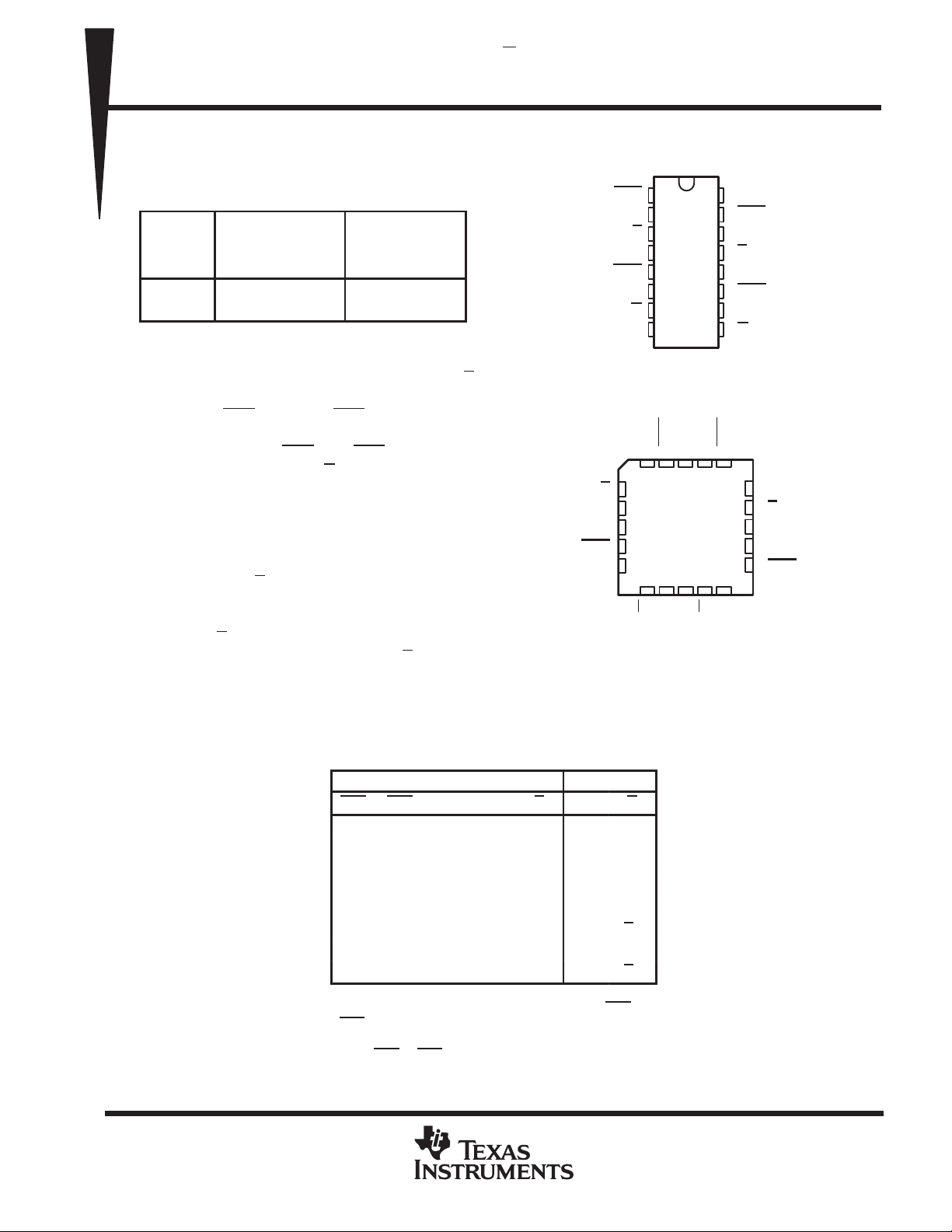
TYPICAL MAXIMUM
TYPE
′ALS109A 50 6
′AS109A 129 29
CLOCK
FREQUENCY
(MHz)
description
These devices contain two independent J-K
positive-edge-triggered flip-flops. A low level at
the preset (PRE
resets the outputs regardless of the levels of the
other inputs. When PRE
(high), data at the J and K
setup-time requirements are transferred to the
outputs on the positive-going edge of the clock
(CLK) pulse. Clock triggering occurs at a voltage
level and is not directly related to the rise time of
the clock pulse. Following the hold-time interval,
data at the J and K
affecting the levels at the outputs. These versatile
flip-flops can perform as toggle flip-flops by
grounding K
perform as D-type flip-flops if J and K
together.
) or clear (CLR) inputs sets or
inputs can be changed without
and tying J high. They also can
TYPICAL POWER
DISSIPATION
PER FLIP-FLOP
and CLR are inactive
inputs meeting the
(mW)
are tied
SN54ALS109A, SN54AS109A ...J PACKAGE
SN74ALS109A, SN74AS109A ...D OR N PACKAGE
SN54ALS109A, SN54AS109A . . . FK PACKAGE
1K
1CLK
NC
1PRE
1Q
NC – No internal connection
(TOP VIEW)
1CLR
1J
1K
1CLK
1PRE
1Q
1Q
GND
(TOP VIEW)
1J
3212019
4
5
6
7
8
910111213
1Q
1
2
3
4
5
6
7
8
1CLR
GND
NC
NC
16
15
14
13
12
11
10
9
V
CC
2Q
V
CC
2CLR
2J
2K
2CLK
2PRE
2Q
2Q
2CLR
18
17
16
15
14
2Q
2J
2K
NC
2CLK
2PRE
The SN54ALS109A and SN54AS109A are characterized for operation over the full military temperature range
of –55°C to 125°C. The SN74ALS109A and SN74AS109A are characterized for operation from 0°C to 70°C.
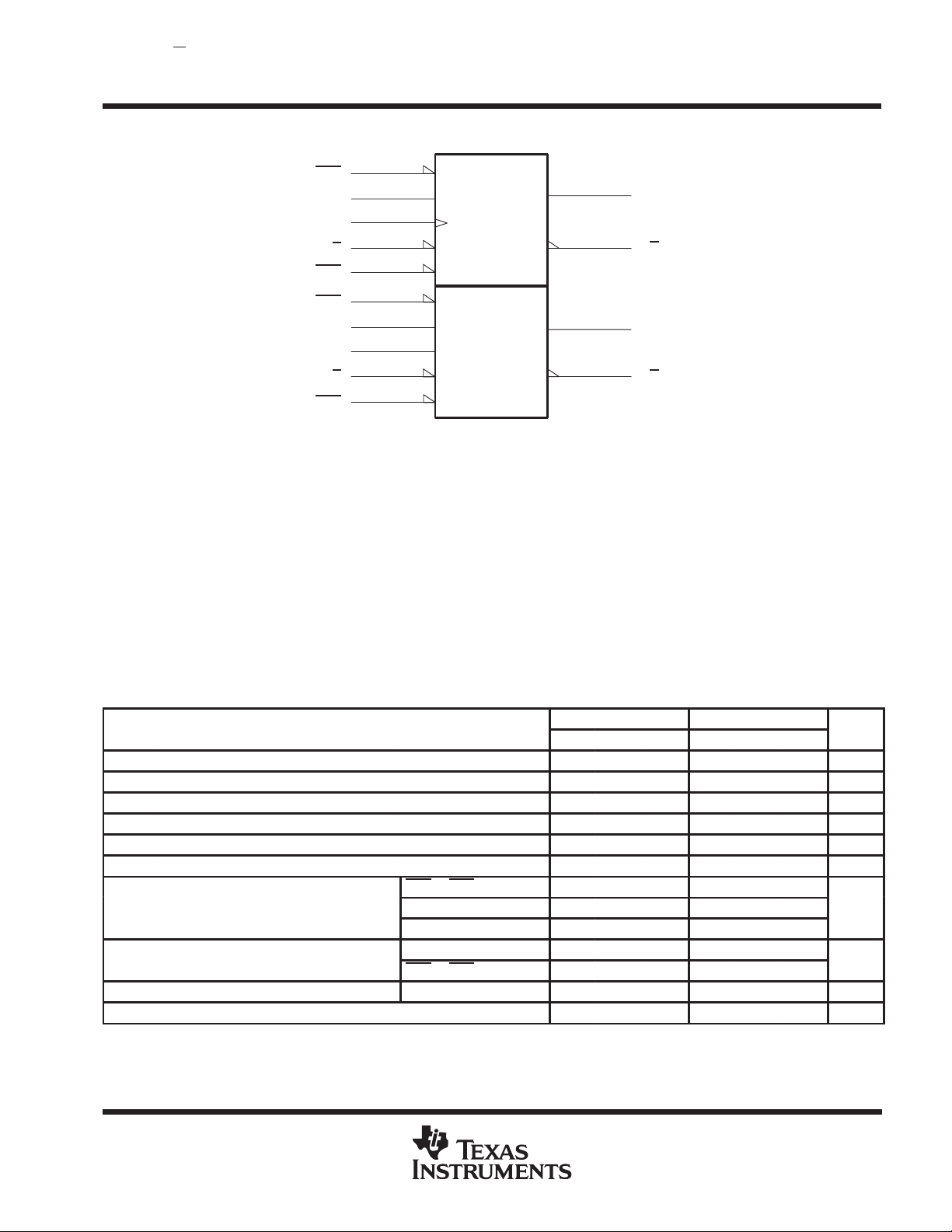
FUNCTION TABLE
PRE CLR CLK J K Q Q
L H X X X H L
H LXXXLH
LLXXXH
HH↑LLLH
HH↑H L Toggle
H H ↑ LHQ0Q0
HH↑HHHL
HHLXXQ0 Q0
†
The output levels in this configuration are not specified to
meet the minimum levels for VOH if the lows at PRE
CLR
configuration is nonstable; that is, it does not persist when
either PRE
PRODUCTION DATA information is current as of publication date.
Products conform to specifications per the terms of Texas Instruments
standard warranty. Production processing does not necessarily include
testing of all parameters.
INPUTS
are near VIL maximum. Furthermore, this
or CLR returns to its inactive (high) level.
OUTPUTS
†
H
†
and
Copyright 1995, Texas Instruments Incorporated
POST OFFICE BOX 655303 • DALLAS, TEXAS 75265
1
SN54ALS109A, SN54AS109A, SN74ALS109A, SN74AS109A
UNIT
t
S
CLK↑
ns
DUAL J-K
POSITIVE-EDGE-TRIGGERED FLIP-FLOPS
WITH CLEAR AND PRESET
SDAS198B – APRIL 1982 – REVISED AUGUST 1995
logic symbol
†
This symbol is in accordance with ANSI/IEEE Std 91-1984 and IEC Publication 617-12.
Pin numbers shown are for the D, J, and N packages.
†
1PRE
1J
1CLK
1K
1CLR
2PRE
2J
2CLK
2K
2CLR
5
2
4
3
1
11
14
12
13
15
S
1J
1K
R
C1
10
6
1Q
7
1Q
2Q
9
2Q
absolute maximum ratings over operating free-air temperature range (unless otherwise noted)
Supply voltage, V
Input voltage, V
Operating free-air temperature range, T
Storage temperature range –65°C to 150°C. . . . . . . . . . . . . . . . . . . . . . . . . . . . . . . . . . . . . . . . . . . . . . . . . . . . . . .
‡
Stresses beyond those listed under “absolute maximum ratings” may cause permanent damage to the device. These are stress ratings only, and
functional operation of the device at these or any other conditions beyond those indicated under “recommended operating conditions” is not
implied. Exposure to absolute-maximum-rated conditions for extended periods may affect device reliability.
7 V. . . . . . . . . . . . . . . . . . . . . . . . . . . . . . . . . . . . . . . . . . . . . . . . . . . . . . . . . . . . . . . . . . . . . . . .
CC
7 V. . . . . . . . . . . . . . . . . . . . . . . . . . . . . . . . . . . . . . . . . . . . . . . . . . . . . . . . . . . . . . . . . . . . . . . . . . . .
I
: SN54ALS109A –55°C to 125°C. . . . . . . . . . . . . . . . . . . . . . . . . . .
A
SN74ALS109A 0°C to 70°C. . . . . . . . . . . . . . . . . . . . . . . . . . . . . . .
‡
recommended operating conditions
V
CC
V
IH
V
IL
I
OH
I
OL
f
clock
t
w
su
t
h
T
A
Supply voltage 4.5 5 5.5 4.5 5 5.5 V
High-level input voltage 2 2 V
Low-level input voltage 0.7 0.8 V
High-level output current –0.4 –0.4 mA
Low-level output current 4 8 mA
Clock frequency 0 30 0 34 MHz
Pulse duration
etup time before
Hold time after CLK↑ Data 0 0 ns
Operating free-air temperature –55 125 0 70 °C
SN54ALS109A SN74ALS109A
MIN NOM MAX MIN NOM MAX
PRE or CLR low 15 15
CLK high 16.5 14.5
CLK low 16.5 14.5
Data 15 15
PRE or CLR inactive 10 10
ns
2
POST OFFICE BOX 655303 • DALLAS, TEXAS 75265
SN54ALS109A, SN54AS109A, SN74ALS109A, SN74AS109A
PARAMETER
TEST CONDITIONS
UNIT
VOLV
4.5 V
V
I
V
V
V
mA
I
V
5.5 V
V
2.7 V
A
I
V
V
V
mA
(INPUT)
(OUTPUT)
PRE
CLR
Q
Q
ns
CLK
Q
Q
ns
DUAL J-K
POSITIVE-EDGE-TRIGGERED FLIP-FLOPS
WITH CLEAR AND PRESET
SDAS198B – APRIL 1982 – REVISED AUGUST 1995
electrical characteristics over recommended operating free-air temperature range (unless
otherwise noted)
SN54ALS109A SN74ALS109A
MIN TYP†MAX MIN TYP†MAX
V
IK
V
OH
I
IH
IL
I
O
I
CC
†
All typical values are at VCC = 5 V, TA = 25°C.
‡
The output conditions have been chosen to produce a current that closely approximates one half of the true short-circuit output current, IOS.
NOTE 1: ICC is measured with J, K
CLK, J, or K
PRE or CLR
CLK, J, or K
PRE or CLR
CLK, J, or K
PRE or CLR
‡
VCC = 4.5 V, II = –18 mA –1.5 –1.5 V
VCC = 4.5 V to 5.5 V, IOH = –0.4 mA VCC–2 VCC–2 V
=
CC
= 5.5 V,
CC
,
=
CC
= 5.5 V,
CC
VCC = 5.5 V, VO = 2.25 V –20 –112 –30 –112 mA
VCC = 5.5 V, See Note 1 2.4 4 2.4 4 mA
, CLK, and PRE grounded, then with J, K, CLK, and CLR grounded.
IOL = 4 mA 0.25 0.4 0.25 0.4
IOL = 8 mA 0.35 0.5
= 7
I
=
I
= 0.4
I
0.1 0.1
0.2 0.2
20 20
40 40
–0.2 –0.2
–0.4 –0.4
µ
switching characteristics (see Figure 1)
VCC = 4.5 V to 5.5 V,
CL = 50 pF,
PARAMETER
f
max
t
PLH
t
PHL
t
PLH
t
§
For conditions shown as MIN or MAX, use the appropriate value specified under recommended operating conditions.
PHL
FROM
INP
or
T
TO
TP
or
or
T
RL = 500 Ω,
TA = MIN to MAX
SN54ALS109A SN74ALS109A
MIN MAX MIN MAX
30 34 MHz
3 17 3 13
5 17 5 15
5 21 5 16
5 20 5 18
§
UNIT
POST OFFICE BOX 655303 • DALLAS, TEXAS 75265
3
SN54ALS109A, SN54AS109A, SN74ALS109A, SN74AS109A
UNIT
tsu*
S
CLK↑
ns
PARAMETER
TEST CONDITIONS
UNIT
I
V
V
V
A
I
V
V
V
mA
DUAL J-K
POSITIVE-EDGE-TRIGGERED FLIP-FLOPS
WITH CLEAR AND PRESET
SDAS198B – APRIL 1982 – REVISED AUGUST 1995
absolute maximum ratings over operating free-air temperature range (unless otherwise noted)
Supply voltage, V
Input voltage, V
Operating free-air temperature range, T
Storage temperature range –65°C to 150°C. . . . . . . . . . . . . . . . . . . . . . . . . . . . . . . . . . . . . . . . . . . . . . . . . . . . . . .
†
Stresses beyond those listed under “absolute maximum ratings” may cause permanent damage to the device. These are stress ratings only, and
functional operation of the device at these or any other conditions beyond those indicated under “recommended operating conditions” is not
implied. Exposure to absolute-maximum-rated conditions for extended periods may affect device reliability.
7 V. . . . . . . . . . . . . . . . . . . . . . . . . . . . . . . . . . . . . . . . . . . . . . . . . . . . . . . . . . . . . . . . . . . . . . . .
CC
7 V. . . . . . . . . . . . . . . . . . . . . . . . . . . . . . . . . . . . . . . . . . . . . . . . . . . . . . . . . . . . . . . . . . . . . . . . . . . .
I
: SN54AS109A –55°C to 125°C. . . . . . . . . . . . . . . . . . . . . . . . . . . . .
A
SN74AS109A 0°C to 70°C. . . . . . . . . . . . . . . . . . . . . . . . . . . . . . . . .
recommended operating conditions
SN54AS109A SN74AS109A
MIN NOM MAX MIN NOM MAX
V
CC
V
IH
V
IL
I
OH
I
OL
f
clock
tw* Pulse duration
th* Hold time after CLK↑ Data 0 0 ns
T
A
* On products compliant to MIL-STD-883, Class B, this parameter is based on characterization data but is not production tested.
Supply voltage 4.5 5 5.5 4.5 5 5.5 V
High-level input voltage 2 2 V
Low-level input voltage 0.8 0.8 V
High-level output current –2 –2 mA
Low-level output current 20 20 mA
* Clock frequency 0 90 0 105 MHz
PRE or CLR low 4 4
CLK high
CLK low 5.5 5.5
*
etup time before
Operating free-air temperature –55 125 0 70 °C
Data 5.5 5.5
PRE or CLR inactive 2 2
4 4
ns
†
electrical characteristics over recommended operating free-air temperature range (unless
otherwise noted)
SN54AS109A SN74AS109A
MIN TYP‡MAX MIN TYP‡MAX
V
IK
V
OH
V
OL
I
I
IH
IL
I
O
I
CC
‡
All typical values are at VCC = 5 V, TA = 25°C.
§
The output conditions have been chosen to produce a current that closely approximates one half of the true short-circuit output current, IOS.
NOTE 1: ICC is measured with J, K
CLK, J, or K
PRE or CLR
CLK, J, or K
PRE or CLR
§
VCC = 4.5 V, II = –18 mA –1.2 –1.2 V
VCC = 4.5 V to 5.5 V, IOH = –2 mA VCC–2 VCC–2 V
VCC = 4.5 V, IOL = 20 mA 0.25 0.5 0.25 0.5 V
VCC = 5.5 V, VI = 7 V 0.1 0.1 mA
= 5.5 V,
CC
= 5.5 V,
CC
VCC = 5.5 V, VO = 2.25 V –30 –112 –30 –112 mA
VCC = 5.5 V, See Note 1 11.5 17 1 1.5 17 mA
, CLK, and PRE grounded, then with J, K, CLK, and CLR grounded.
= 2.7
I
= 0.4
I
20 20
40 40
–0.5 –0.5
–1.8 –1.8
µ
4
POST OFFICE BOX 655303 • DALLAS, TEXAS 75265

SN54ALS109A, SN54AS109A, SN74ALS109A, SN74AS109A
(
)
(OUTPUT)
(INPUT)
(OUTPUT)
PRE
CLR
Q
Q
ns
CLK
Q
Q
ns
DUAL J-K
POSITIVE-EDGE-TRIGGERED FLIP-FLOPS
WITH CLEAR AND PRESET
SDAS198B – APRIL 1982 – REVISED AUGUST 1995
switching characteristics (see Figure 1)
VCC = 4.5 V to 5.5 V,
CL = 50 pF,
PARAMETER
f
* 90 105 MHz
max
t
PLH
t
PHL
t
PLH
t
PHL
* On products compliant to MIL-STD-883, Class B, this parameter is based on characterization data but is not production tested.
†
For conditions shown as MIN or MAX, use the appropriate value specified under recommended operating conditions.
FROM
INPUT
or
TO
or
or
RL = 500 Ω,
TA = MIN to MAX
SN54AS109A SN74AS109A
MIN MAX MIN MAX
2 9 2 8
3.5 11.5 3.5 10.5
2.5 10 2.5 9
3.5 10.5 3.5 9
†
UNIT
POST OFFICE BOX 655303 • DALLAS, TEXAS 75265
5

SN54ALS109A, SN54AS109A, SN74ALS109A, SN74AS109A
DUAL J-K
POSITIVE-EDGE-TRIGGERED FLIP-FLOPS
WITH CLEAR AND PRESET
SDAS198B – APRIL 1982 – REVISED AUGUST 1995
PARAMETER MEASUREMENT INFORMATION
SERIES 54ALS/74ALS AND 54AS/74AS DEVICES
V
CC
R
L
From Output
Under Test
(see Note A)
C
L
Test
Point
R
L
From Output
Under Test
C
(see Note A)
Test
Point
L
From Output
Under Test
(see Note A)
7 V
RL = R1 = R2
S1
R1
C
L
Test
Point
R2
LOAD CIRCUIT FOR
BI-STATE
TOTEM-POLE OUTPUTS
Timing
Input
t
su
Data
Input
VOLTAGE WAVEFORMS
SETUP AND HOLD TIMES
Output
Control
(low-level
enabling)
Waveform 1
S1 Closed
(see Note B)
Waveform 2
S1 Open
(see Note B)
t
PZL
t
PZH
ENABLE AND DISABLE TIMES, 3-STATE OUTPUTS
VOLTAGE WAVEFORMS
1.3 V
t
PHZ
1.3 V
1.3 V
t
1.3 V1.3 V
1.3 V1.3 V
FOR OPEN-COLLECTOR OUTPUTS
h
t
PLZ
LOAD CIRCUIT
3.5 V
0.3 V
3.5 V
0.3 V
3.5 V
0.3 V
[
3.5 V
V
OL
0.3 V
V
OH
0.3 V
[
0 V
High-Level
Low-Level
Out-of-Phase
(see Note C)
Pulse
Pulse
Input
In-Phase
Output
Output
LOAD CIRCUIT
FOR 3-STATE OUTPUTS
1.3 V 1.3 V
t
w
1.3 V 1.3 V
VOLTAGE WAVEFORMS
PULSE DURATIONS
1.3 V 1.3 V
t
PLH
t
PHL
1.3 V 1.3 V
VOLTAGE WAVEFORMS
PROPAGATION DELAY TIMES
1.3 V1.3 V
t
PHL
t
PLH
3.5 V
0.3 V
3.5 V
0.3 V
3.5 V
0.3 V
V
V
V
V
OH
OL
OH
OL
NOTES: A. CL includes probe and jig capacitance.
B. Waveform 1 is for an output with internal conditions such that the output is low except when disabled by the output control.
Waveform 2 is for an output with internal conditions such that the output is high except when disabled by the output control.
C. When measuring propagation delay items of 3-state outputs, switch S1 is open.
D. All input pulses have the following characteristics: PRR ≤ 1 MHz, tr = tf = 2 ns, duty cycle = 50%.
E. The outputs are measured one at a time with one transition per measurement.
Figure 1. Load Circuits and Voltage Waveforms
6
POST OFFICE BOX 655303 • DALLAS, TEXAS 75265

IMPORTANT NOTICE
T exas Instruments and its subsidiaries (TI) reserve the right to make changes to their products or to discontinue
any product or service without notice, and advise customers to obtain the latest version of relevant information
to verify, before placing orders, that information being relied on is current and complete. All products are sold
subject to the terms and conditions of sale supplied at the time of order acknowledgement, including those
pertaining to warranty, patent infringement, and limitation of liability.
TI warrants performance of its semiconductor products to the specifications applicable at the time of sale in
accordance with TI’s standard warranty. Testing and other quality control techniques are utilized to the extent
TI deems necessary to support this warranty . Specific testing of all parameters of each device is not necessarily
performed, except those mandated by government requirements.
CERT AIN APPLICATIONS USING SEMICONDUCTOR PRODUCTS MAY INVOLVE POTENTIAL RISKS OF
DEATH, PERSONAL INJURY, OR SEVERE PROPERTY OR ENVIRONMENTAL DAMAGE (“CRITICAL
APPLICATIONS”). TI SEMICONDUCTOR PRODUCTS ARE NOT DESIGNED, AUTHORIZED, OR
WARRANTED TO BE SUITABLE FOR USE IN LIFE-SUPPORT DEVICES OR SYSTEMS OR OTHER
CRITICAL APPLICA TIONS. INCLUSION OF TI PRODUCTS IN SUCH APPLICATIONS IS UNDERST OOD TO
BE FULLY AT THE CUSTOMER’S RISK.
In order to minimize risks associated with the customer’s applications, adequate design and operating
safeguards must be provided by the customer to minimize inherent or procedural hazards.
TI assumes no liability for applications assistance or customer product design. TI does not warrant or represent
that any license, either express or implied, is granted under any patent right, copyright, mask work right, or other
intellectual property right of TI covering or relating to any combination, machine, or process in which such
semiconductor products or services might be or are used. TI’s publication of information regarding any third
party’s products or services does not constitute TI’s approval, warranty or endorsement thereof.
Copyright 1998, Texas Instruments Incorporated
 Loading...