

SN54ALS874B, SN74ALS874B, SN74ALS876A
SN74AS874, SN74AS876
DUAL 4-BIT D-TYPE EDGE-TRIGGERED FLIP-FLOPS
SDAS061C – APRIL 1982 – REVISED JANUARY 1995
• 3-State Buffer-Type Outputs Drive Bus
Lines Directly
• Bus-Structured Pinout
• Choice of True or Inverting Logic
– SN54ALS874B, SN74ALS874B,
SN74AS874 Have True Outputs
– SN74ALS876A, SN74AS876 Have
Inverting Outputs
• Asynchronous Clear
• Package Options Include Plastic
Small-Outline (DW) Packages, Plastic (FN)
and Ceramic (FK) Chip Carriers, and
Standard Plastic (NT) and Ceramic (JT)
300-mil DIPs
description
These dual 4-bit D-type edge-triggered flip-flops
feature 3-state outputs designed specifically as
bus drivers. They are particularly suitable for
implementing buffer registers, I/O ports,
bidirectional bus drivers, and working registers.
The edge-triggered flip-flops enter data on the
low-to-high transition of the clock (CLK) input.
The SN54ALS874B, SN74ALS874B, and
SN74AS874 have clear (CLR
noninverting Q outputs. The SN74ALS876A and
SN74AS876 have preset (PRE
inverting Q
four Q or Q
outputs; taking PRE low causes the
outputs to go low independently of the
clock.
The SN54ALS874B is characterized for operation
over the full military temperature range of –55°C
to 125°C. The SN74ALS874B, SN74ALS876A,
SN74AS874, and SN74AS876 devices are
characterized for operation from 0°C to 70°C.
) inputs and
) inputs and
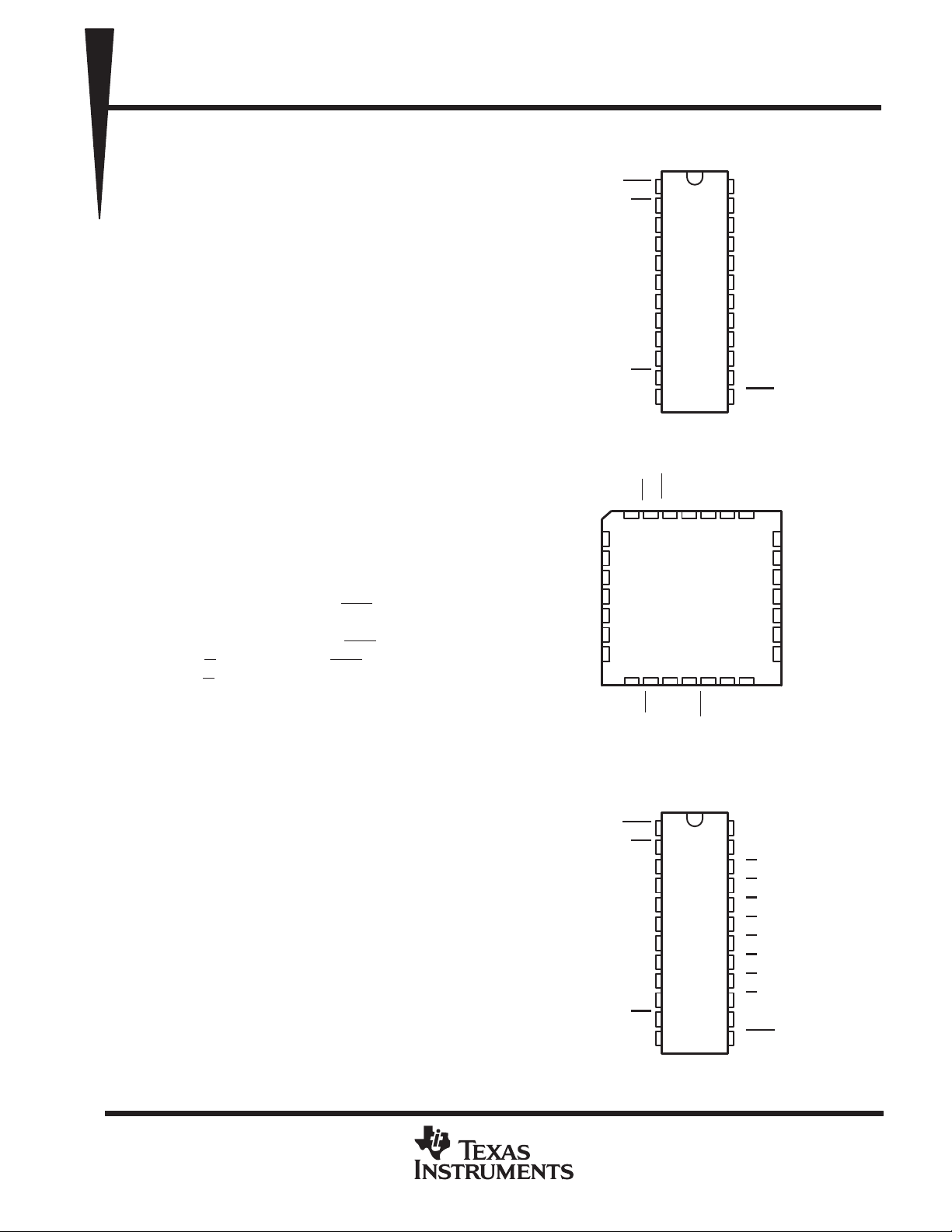
SN74ALS874B, SN74AS874 . . . DW OR NT PACKAGE
SN74ALS876A, SN74AS876 . . . DW OR NT PACKAGE
SN54ALS874B ...JT PACKAGE
(TOP VIEW)
1
2
3
4
5
6
7
8
9
10
11
12
1CLR
NC
28 27 26
15 16 17 18
NC
GND
1
2
3
4
5
6
7
8
9
10
11
12
24
23
22
21
20
19
18
17
16
15
14
13
CC
V
2CLR
24
23
22
21
20
19
18
17
16
15
14
13
1CLR
1OE
1D1
1D2
1D3
1D4
2D1
2D2
2D3
2D4
2OE
GND
SN54ALS874B . . . FK PACKAGE
1D2
5
1D3
6
1D4
7
NC
8
2D1
9
2D2
10
2D3
11
NC – No internal connection
4
12
1D1
13 14
2D4
(TOP VIEW)
1OE
321
2OE
(TOP VIEW)
1PRE
1OE
1D1
1D2
1D3
1D4
2D1
2D2
2D3
2D4
2OE
GND
V
CC
1CLK
1Q1
1Q2
1Q3
1Q4
2Q1
2Q2
2Q3
2Q4
2CLK
2CLR
1CLK
1Q1
2Q4
2CLK
V
CC
1CLK
1Q
1Q
1Q3
1Q
2Q
2Q
2Q3
2Q
2CLK
2PRE
25
24
23
22
21
20
19
1
2
4
1
2
4
1Q2
1Q3
1Q4
NC
2Q1
2Q2
2Q3
PRODUCTION DATA information is current as of publication date.
Products conform to specifications per the terms of Texas Instruments
standard warranty. Production processing does not necessarily include
testing of all parameters.
POST OFFICE BOX 655303 • DALLAS, TEXAS 75265
Copyright 1995, Texas Instruments Incorporated
1
SN54ALS874B, SN74ALS874B, SN74ALS876A
SN74AS874, SN74AS876
DUAL 4-BIT D-TYPE EDGE-TRIGGERED FLIP-FLOPS
SDAS061C – APRIL 1982 – REVISED JANUARY 1995
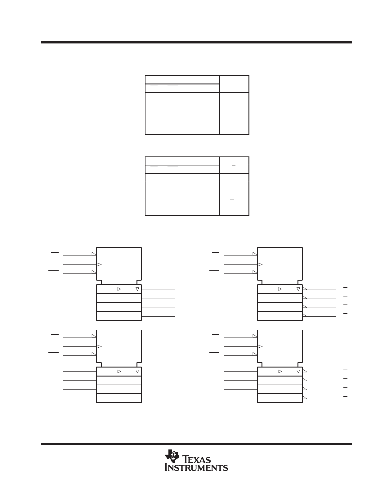
Function Tables
logic symbols
SN54ALS874B, SN74ALS874B, SN74AS874
SN54ALS874B, SN74ALS874B, SN74AS874
OE CLR CLK D
L L X X L
L H ↑ HH
LH↑LL
LHLX Q
HXXX Z
OE PRE CLK D
L L X X L
L H ↑ HL
LH↑LH
LHLX Q
HXXX Z
(each flip-flop)
INPUTS
SN74ALS876A, SN74AS876
(each flip-flop)
INPUTS
OUTPUT
OUTPUT
Q
0
Q
0
†
SN74ALS876A, SN74AS876
2
1OE
1D1
1D2
1D3
1D4
2OE
2D1
2D2
2D3
2D4
23
1
3
4
5
6
11
14
13
7
8
9
10
1CLK
1CLR
2CLK
2CLR
†
These symbols are in accordance with ANSI/IEEE Std 91-1984 and IEC Publication 617-12.
Pin numbers shown are for the DW, JT, and NT packages.
EN
R
1D
EN
R
1D
C1
C1
22
21
20
19
18
17
16
15
1CLK
1PRE
1Q1
1Q2
1Q3
1Q4
2CLK
2PRE
2Q1
2Q2
2Q3
2Q4
1OE
1D1
1D2
1D3
1D4
2OE
2D1
2D2
2D3
2D4
2
23
1
3
4
5
6
11
14
13
7
8
9
10
EN
S
1D
EN
S
1D
C1
C1
22
21
20
19
18
17
16
15
1Q1
1Q
1Q
1Q
2Q
2Q
2Q
2Q
2
3
4
1
2
3
4
2
POST OFFICE BOX 655303 • DALLAS, TEXAS 75265
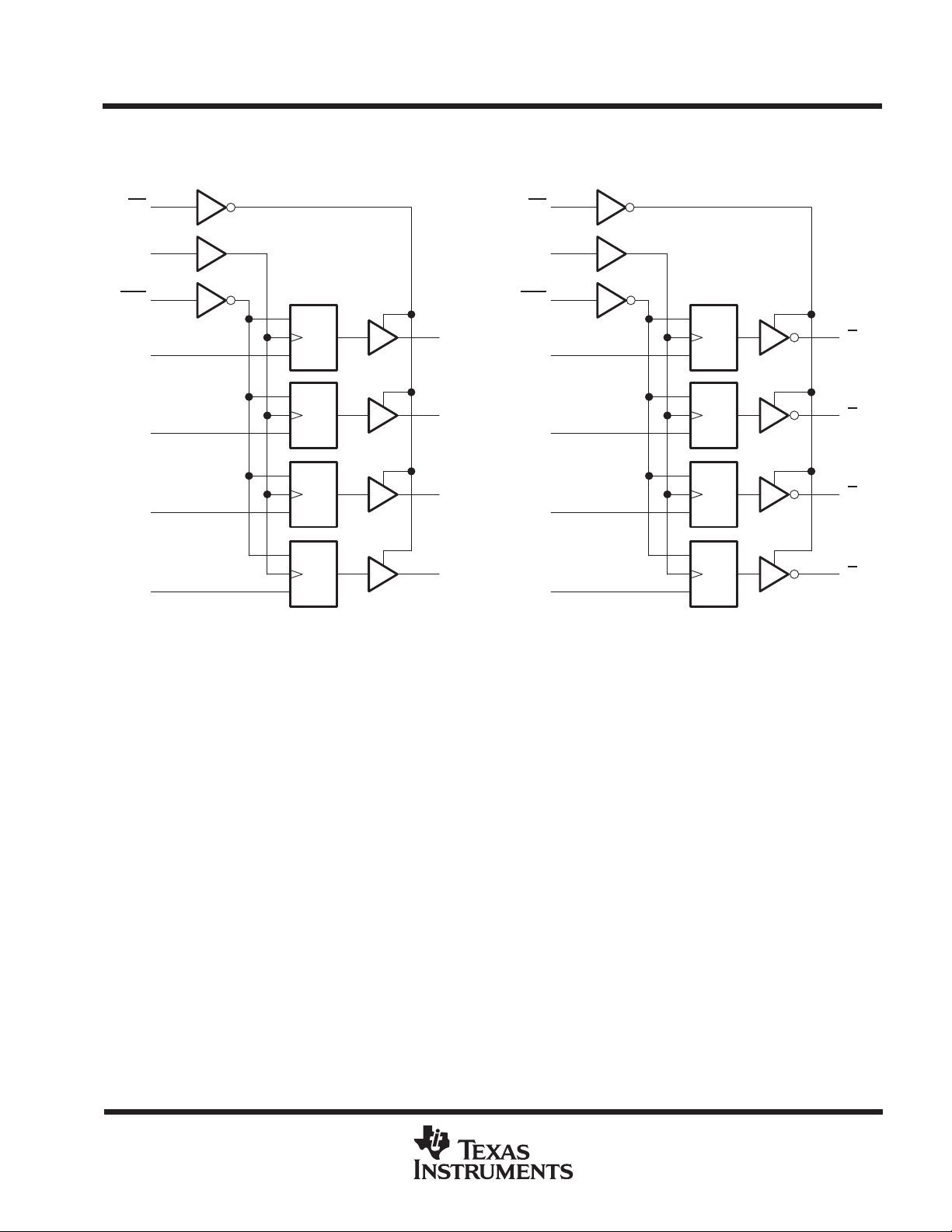
logic diagrams (positive logic)
SN54ALS874B, SN74ALS874B, SN74ALS876A
SN74AS874, SN74AS876
DUAL 4-BIT D-TYPE EDGE-TRIGGERED FLIP-FLOPS
SDAS061C – APRIL 1982 – REVISED JANUARY 1995
SN54ALS874B, SN74ALS874B, SN74AS874
OE
CLK
CLR
D1
D2
D3
D4
(each quad flip-flop)
R
C1
1D
R
C1
1D
R
C1
1D
R
C1
1D
Q1
Q2
Q3
Q4
OE
CLK
PRE
D1
D2
D3
D4
SN74ALS876A, SN74AS876
(each quad flip-flop)
S
C1
1D
S
C1
1D
S
C1
1D
S
C1
1D
Q
1
Q
2
Q
3
Q
4
Pin numbers shown are for the DW, JT, and NT packages.
absolute maximum ratings over operating free-air temperature range (unless otherwise noted)
Supply voltage, V
Input voltage, V
Voltage applied to a disabled 3-state output 5.5 V. . . . . . . . . . . . . . . . . . . . . . . . . . . . . . . . . . . . . . . . . . . . . . . . . .
Operating free-air temperature range, T
Storage temperature range –65°C to 150°C. . . . . . . . . . . . . . . . . . . . . . . . . . . . . . . . . . . . . . . . . . . . . . . . . . . . . . .
†
Stresses beyond those listed under “absolute maximum ratings” may cause permanent damage to the device. These are stress ratings only, and
functional operation of the device at these or any other conditions beyond those indicated under “recommended operating conditions” is not
implied. Exposure to absolute-maximum-rated conditions for extended periods may affect device reliability.
7 V. . . . . . . . . . . . . . . . . . . . . . . . . . . . . . . . . . . . . . . . . . . . . . . . . . . . . . . . . . . . . . . . . . . . . . . .
CC
7 V. . . . . . . . . . . . . . . . . . . . . . . . . . . . . . . . . . . . . . . . . . . . . . . . . . . . . . . . . . . . . . . . . . . . . . . . . . . .
I
: SN54ALS874B –55°C to 125°C. . . . . . . . . . . . . . . . . . . . . . . . . . .
A
SN74ALS874B, SN74ALS876A 0°C to 70°C. . . . . . . . . . . . . . . . .
†
POST OFFICE BOX 655303 • DALLAS, TEXAS 75265
3
SN54ALS874B, SN74ALS874B, SN74ALS876A
t
S
CLK↑
ns
V
4.5 V
VOLV
4.5 V
V
I
mA
SN74AS874, SN74AS876
DUAL 4-BIT D-TYPE EDGE-TRIGGERED FLIP-FLOPS
SDAS061C – APRIL 1982 – REVISED JANUARY 1995
recommended operating conditions
V
CC
V
IH
V
IL
I
OH
I
OL
f
clock
t
w
su
t
h
T
A
Supply voltage 4.5 5 5.5 4.5 5 5.5 V
High-level input voltage 2 2 V
Low-level input voltage 0.7 0.8 V
High-level output current –1 –2.6 mA
Low-level output current 12 24 mA
Clock frequency 0 25 0 30 MHz
PRE or CLR low 15 10
Pulse duration
etup time before
Hold time, data after CLK↑ 4 0 ns
Operating free-air temperature –55 125 0 70 °C
CLK high 20 16.5
CLK low 20 16.5
Data 15 15
PRE or CLR inactive 15 10
SN54ALS874B
MIN NOM MAX MIN NOM MAX
SN74ALS874B
SN74ALS876A
UNIT
ns
electrical characteristics over recommended operating free-air temperature range (unless
otherwise noted)
PARAMETER TEST CONDITIONS
V
IK
V
OH
I
OZH
I
OZL
I
I
I
IH
I
IL
‡
I
O
′ALS874B VCC = 5.5 V
CC
SN74ALS876A VCC = 5.5 V
†
All typical values are at VCC = 5 V, TA = 25°C.
‡
The output conditions have been chosen to produce a current that closely approximates one half of the true short-circuit output current, IOS.
VCC = 4.5 V, II = –18 mA –1.2 –1.2 V
VCC = 4.5 V to 5.5 V, IOH = –0.4 mA VCC –2 VCC –2
=
CC
=
CC
VCC = 5.5 V, VO = 2.7 V 20 20 µA
VCC = 5.5 V, VO = 0.4 V –20 –20 µA
VCC = 5.5 V, VI = 7 V 0.1 0.1 mA
VCC = 5.5 V, VI = 2.7 V 20 20 µA
VCC = 5.5 V, VI = 0.4 V –0.2 –0.2 mA
VCC = 5.5 V, VO = 2.25 V –20 –112 –30 –112 mA
IOH = –1 mA 2.4 3.3
IOH = –2.6 mA 2.4 3.2
IOL = 12 mA 0.25 0.4 0.25 0.4
IOL = 24 mA 0.35 0.5
Outputs high 14 21 14 21
Outputs low 19 30 19 30
Outputs disabled 20 32 20 32
Outputs high 14 21
Outputs low 18 29
Outputs disabled 20 31
SN54ALS874B
MIN TYP†MAX MIN TYP†MAX
SN74ALS874B
SN74ALS876A
UNIT
V
4
POST OFFICE BOX 655303 • DALLAS, TEXAS 75265
SN54ALS874B, SN74ALS874B, SN74ALS876A
CLK
A
Q
ns
OE
A
Q
ns
OE
A
Q
ns
CLK
A
Q
ns
OE
A
Q
ns
OE
A
Q
ns
SN74AS874, SN74AS876
DUAL 4-BIT D-TYPE EDGE-TRIGGERED FLIP-FLOPS
SDAS061C – APRIL 1982 – REVISED JANUARY 1995
switching characteristics (see Figure 1)
VCC = 4.5 V to 5.5 V,
CL = 50 pF,
PARAMETER
f
max
t
PLH
t
PHL
t
PHL
t
PZH
t
PZL
t
PHZ
t
†
For conditions shown as MIN or MAX, use the appropriate value specified under recommended operating conditions.
PLZ
FROM
(INPUT)
CLR
TO
(OUTPUT)
ny
Any Q
ny
ny
switching characteristics (see Figure 1)
PARAMETER
f
max
t
PLH
t
PHL
t
PHL
t
PZH
t
PZL
t
PHZ
t
†
For conditions shown as MIN or MAX, use the appropriate value specified under recommended operating conditions.
PLZ
FROM
(INPUT)
PRE
TO
(OUTPUT)
ny
Any Q
ny
ny
R1 = 500 Ω
R2 = 500 Ω,
TA = MIN to MAX
SN54ALS874B SN74ALS874B
MIN MAX MIN MAX
25 30 MHz
4 18 4 14
4 16 4 14
5 23 5 17 ns
4 24 4 18
4 21 4 18
2 15 2 10
3 22 3 12
VCC = 4.5 V to 5.5 V,
CL = 50 pF,
R1 = 500 Ω
R2 = 500 Ω,
TA = MIN to MAX
SN74ALS876A
,
†
,
†
MIN MAX
30 MHz
4 14
4 14
6 19 ns
4 18
4 18
2 10
3 13
UNIT
UNIT
absolute maximum ratings over operating free-air temperature range (unless otherwise noted)
Supply voltage, V
Input voltage, V
Operating free-air temperature range, T
Storage temperature range –65°C to 150°C. . . . . . . . . . . . . . . . . . . . . . . . . . . . . . . . . . . . . . . . . . . . . . . . . . . . . . .
‡
Stresses beyond those listed under “absolute maximum ratings” may cause permanent damage to the device. These are stress ratings only, and
functional operation of the device at these or any other conditions beyond those indicated under “recommended operating conditions” is not
implied. Exposure to absolute-maximum-rated conditions for extended periods may affect device reliability.
7 V. . . . . . . . . . . . . . . . . . . . . . . . . . . . . . . . . . . . . . . . . . . . . . . . . . . . . . . . . . . . . . . . . . . . . . . .
CC
7 V. . . . . . . . . . . . . . . . . . . . . . . . . . . . . . . . . . . . . . . . . . . . . . . . . . . . . . . . . . . . . . . . . . . . . . . . . . . .
I
: SN74AS874, SN74AS876 0°C to 70°C. . . . . . . . . . . . . . . . . . . . . .
A
POST OFFICE BOX 655303 • DALLAS, TEXAS 75265
‡
5
SN54ALS874B, SN74ALS874B, SN74ALS876A
UNIT
t
S
CLK↑
ns
V
V
I
V
5.5 V
V
0.4 V
mA
I
mA
SN74AS874, SN74AS876
DUAL 4-BIT D-TYPE EDGE-TRIGGERED FLIP-FLOPS
SDAS061C – APRIL 1982 – REVISED JANUARY 1995
recommended operating conditions
V
CC
V
IH
V
IL
I
OH
I
OL
f
clock
t
w
su
t
h
T
A
Supply voltage 4.5 5 5.5 4.5 5 5.5 V
High-level input voltage 2 2 V
Low-level input voltage 0.8 0.8 V
High-level output current –15 –15 mA
Low-level output current 48 48 mA
Clock frequency 0 125 0 80 MHz
PRE or CLR low 2 4.5
Pulse duration
etup time before
Hold time, data after CLK↑ 1 2 ns
Operating free-air temperature 0 70 0 70 °C
CLK high
CLK low 4 6.2
Data 2 4.5
PRE or CLR inactive 4 5
SN74AS874 SN74AS876
MIN NOM MAX MIN NOM MAX
3 6.2
ns
electrical characteristics over recommended operating free-air temperature range (unless
otherwise noted)
SN74AS874
PARAMETER TEST CONDITIONS
V
IK
OH
V
OL
I
OZH
I
OZL
I
I
I
IH
IL
I
O
CC
†
All typical values are at VCC = 5 V, TA = 25°C.
‡
The output conditions have been chosen to produce a current that closely approximates one half of the true short-circuit output current, IOS.
D
All others
‡
SN74AS874 VCC = 5.5 V
SN74AS876 VCC = 5.5 V
VCC = 4.5 V, II = –18 mA –1.2 V
VCC = 4.5 V to 5.5 V, IOH = –2 mA VCC –2
VCC = 4.5 V, IOH = –15 mA 2.4 3.3
VCC = 4.5 V, IOL = 48 mA 0.35 0.5 V
VCC = 5.5 V, VO = 2.7 V 50 µA
VCC = 5.5 V, VO = 0.4 V –50 µA
VCC = 5.5 V, VI = 7 V 0.1 mA
VCC = 5.5 V, VI = 2.7 V 20 µA
,
=
CC
VCC = 5.5 V, VO = 2.25 V –30 –112 mA
=
I
Outputs high 82 133
Outputs low 92 149
Outputs disabled 100 160
Outputs high 88 142
Outputs low 94 150
Outputs disabled 100 160
SN74AS876
MIN TYP†MAX
–2
–0.5
UNIT
6
POST OFFICE BOX 655303 • DALLAS, TEXAS 75265

SN54ALS874B, SN74ALS874B, SN74ALS876A
CLK
A
Q
ns
OE
A
Q
ns
OE
A
Q
ns
CLK
A
Q
ns
OE
A
Q
ns
OE
A
Q
ns
SN74AS874, SN74AS876
DUAL 4-BIT D-TYPE EDGE-TRIGGERED FLIP-FLOPS
SDAS061C – APRIL 1982 – REVISED JANUARY 1995
switching characteristics (see Figure 1)
VCC = 4.5 V to 5.5 V,
CL = 50 pF,
PARAMETER
f
max
t
PLH
t
PHL
t
PHL
t
PZH
t
PZL
t
PHZ
t
†
For conditions shown as MIN or MAX, use the appropriate value specified under recommended operating conditions.
PLZ
FROM
(INPUT)
CLR
TO
(OUTPUT)
ny
Any Q
ny
ny
switching characteristics (see Figure 1)
PARAMETER
f
max
t
PLH
t
PHL
t
PHL
t
PZH
t
PZL
t
PHZ
t
†
For conditions shown as MIN or MAX, use the appropriate value specified under recommended operating conditions.
PLZ
FROM
(INPUT)
PRE
TO
(OUTPUT)
ny
Any Q
ny
ny
R1 = 500 Ω
R2 = 500 Ω,
TA = MIN to MAX
VCC = 4.5 V to 5.5 V,
CL = 50 pF,
R1 = 500 Ω
R2 = 500 Ω,
TA = MIN to MAX
,
UNIT
†
SN74AS874
MIN MAX
125 MHz
3 8.5
4 10.5
4 9.5 ns
2 7
3 10.5
2 6
2 7.5
,
UNIT
†
SN74AS876
MIN MAX
80 MHz
3 8.5
4 10.5
4 9.5 ns
2 7
3 11
2 7
2 7
POST OFFICE BOX 655303 • DALLAS, TEXAS 75265
7

SN54ALS874B, SN74ALS874B, SN74ALS876A
SN74AS874, SN74AS876
DUAL 4-BIT D-TYPE EDGE-TRIGGERED FLIP-FLOPS
SDAS061C – APRIL 1982 – REVISED JANUARY 1995
PARAMETER MEASUREMENT INFORMATION
SERIES 54ALS/74ALS AND 54AS/74AS DEVICES
V
CC
R
L
From Output
Under Test
(see Note A)
C
L
Test
Point
R
L
From Output
Under Test
(see Note A)
Test
Point
C
L
From Output
Under Test
(see Note A)
7 V
RL = R1 = R2
S1
R1
C
L
Test
Point
R2
LOAD CIRCUIT FOR
BI-STATE
TOTEM-POLE OUTPUTS
Timing
Input
t
su
Data
Input
VOLTAGE WAVEFORMS
SETUP AND HOLD TIMES
Output
Control
(low-level
enabling)
Waveform 1
S1 Closed
(see Note B)
Waveform 2
S1 Open
(see Note B)
t
PZL
t
PZH
ENABLE AND DISABLE TIMES, 3-STATE OUTPUTS
VOLTAGE WAVEFORMS
1.3 V
t
PHZ
1.3 V
1.3 V
t
1.3 V1.3 V
1.3 V1.3 V
FOR OPEN-COLLECTOR OUTPUTS
h
t
PLZ
LOAD CIRCUIT
3.5 V
0.3 V
3.5 V
0.3 V
3.5 V
0.3 V
[
3.5 V
V
OL
0.3 V
V
OH
0.3 V
[
0 V
High-Level
Low-Level
Out-of-Phase
(see Note C)
Pulse
Pulse
Input
In-Phase
Output
Output
LOAD CIRCUIT
FOR 3-STATE OUTPUTS
1.3 V 1.3 V
t
w
1.3 V 1.3 V
VOLTAGE WAVEFORMS
PULSE DURATIONS
1.3 V 1.3 V
t
PLH
t
PHL
1.3 V 1.3 V
VOLTAGE WAVEFORMS
PROPAGATION DELAY TIMES
1.3 V1.3 V
t
PHL
t
PLH
3.5 V
0.3 V
3.5 V
0.3 V
3.5 V
0.3 V
V
V
V
V
OH
OL
OH
OL
NOTES: A. CL includes probe and jig capacitance.
B. Waveform 1 is for an output with internal conditions such that the output is low except when disabled by the output control.
Waveform 2 is for an output with internal conditions such that the output is high except when disabled by the output control.
C. When measuring propagation delay items of 3-state outputs, switch S1 is open.
D. All input pulses have the following characteristics: PRR ≤ 1 MHz, tr = tf = 2 ns, duty cycle = 50%.
E. The outputs are measured one at a time with one transition per measurement.
Figure 1. Load Circuits and Voltage Waveforms
8
POST OFFICE BOX 655303 • DALLAS, TEXAS 75265

PACKAGE OPTION ADDENDUM
www.ti.com
PACKAGING INFORMATION
Orderable Device Status
84010013A ACTIVE LCCC FK 28 1 TBD POST-PLATE N / A for Pkg Type
8401001KA OBSOLETE CFP W 24 TBD Call TI Call TI
8401001LA ACTIVE CDIP JT 24 1 TBD A42 SNPB N / A for Pkg Type
SN54ALS874BJT ACTIVE CDIP JT 24 1 TBD A42 SNPB N / A for Pkg Type
SN74ALS874BDW ACTIVE SOIC DW 24 25 Green (RoHS &
SN74ALS874BDWE4 ACTIVE SOIC DW 24 25 Green (RoHS &
SN74ALS874BDWG4 ACTIVE SOIC DW 24 25 Green (RoHS &
SN74ALS874BDWR ACTIVE SOIC DW 24 2000 Green (RoHS &
SN74ALS874BDWRE4 ACTIVE SOIC DW 24 2000 Green (RoHS &
SN74ALS874BDWRG4 ACTIVE SOIC DW 24 2000 Green (RoHS &
SN74ALS874BNSR ACTIVE SO NS 24 2000 Green (RoHS &
SN74ALS874BNSRE4 ACTIVE SO NS 24 2000 Green (RoHS &
SN74ALS874BNSRG4 ACTIVE SO NS 24 2000 Green (RoHS &
SN74ALS874BNT ACTIVE PDIP NT 24 15 Pb-Free
SN74ALS874BNTE4 ACTIVE PDIP NT 24 15 Pb-Free
SN74ALS876ADW ACTIVE SOIC DW 24 25 Green (RoHS &
SN74ALS876ADWE4 ACTIVE SOIC DW 24 25 Green (RoHS &
SN74ALS876ADWG4 ACTIVE SOIC DW 24 25 Green (RoHS &
SN74ALS876ADWR ACTIVE SOIC DW 24 2000 Green (RoHS &
SN74ALS876ADWRE4 ACTIVE SOIC DW 24 2000 Green (RoHS &
SN74ALS876ADWRG4 ACTIVE SOIC DW 24 2000 Green (RoHS &
SN74ALS876ANT ACTIVE PDIP NT 24 15 Pb-Free
SN74ALS876ANTE4 ACTIVE PDIP NT 24 15 Pb-Free
SN74AS874DW ACTIVE SOIC DW 24 25 Green (RoHS &
SN74AS874DWE4 ACTIVE SOIC DW 24 25 Green (RoHS &
SN74AS874DWG4 ACTIVE SOIC DW 24 25 Green (RoHS &
SN74AS874DWR ACTIVE SOIC DW 24 2000 Green (RoHS & CU NIPDAU Level-1-260C-UNLIM
(1)
Package
Type
Package
Drawing
Pins Package
Qty
Eco Plan
no Sb/Br)
no Sb/Br)
no Sb/Br)
no Sb/Br)
no Sb/Br)
no Sb/Br)
no Sb/Br)
no Sb/Br)
no Sb/Br)
no Sb/Br)
no Sb/Br)
no Sb/Br)
no Sb/Br)
no Sb/Br)
no Sb/Br)
no Sb/Br)
no Sb/Br)
no Sb/Br)
(RoHS)
(RoHS)
(RoHS)
(RoHS)
(2)
Lead/Ball Finish MSL Peak Temp
CU NIPDAU Level-1-260C-UNLIM
CU NIPDAU Level-1-260C-UNLIM
CU NIPDAU Level-1-260C-UNLIM
CU NIPDAU Level-1-260C-UNLIM
CU NIPDAU Level-1-260C-UNLIM
CU NIPDAU Level-1-260C-UNLIM
CU NIPDAU Level-1-260C-UNLIM
CU NIPDAU Level-1-260C-UNLIM
CU NIPDAU Level-1-260C-UNLIM
CU NIPDAU N / A for Pkg Type
CU NIPDAU N / A for Pkg Type
CU NIPDAU Level-1-260C-UNLIM
CU NIPDAU Level-1-260C-UNLIM
CU NIPDAU Level-1-260C-UNLIM
CU NIPDAU Level-1-260C-UNLIM
CU NIPDAU Level-1-260C-UNLIM
CU NIPDAU Level-1-260C-UNLIM
CU NIPDAU N / A for Pkg Type
CU NIPDAU N / A for Pkg Type
CU NIPDAU Level-1-260C-UNLIM
CU NIPDAU Level-1-260C-UNLIM
CU NIPDAU Level-1-260C-UNLIM
9-Oct-2007
(3)
Addendum-Page 1

PACKAGE OPTION ADDENDUM
www.ti.com
Orderable Device Status
(1)
Package
Type
Package
Drawing
Pins Package
Qty
Eco Plan
(2)
Lead/Ball Finish MSL Peak Temp
9-Oct-2007
(3)
no Sb/Br)
SN74AS874DWRE4 ACTIVE SOIC DW 24 2000 Green (RoHS &
CU NIPDAU Level-1-260C-UNLIM
no Sb/Br)
SN74AS874DWRG4 ACTIVE SOIC DW 24 2000 Green (RoHS &
CU NIPDAU Level-1-260C-UNLIM
no Sb/Br)
SN74AS874NT ACTIVE PDIP NT 24 15 Pb-Free
CU NIPDAU N / A for Pkg Type
(RoHS)
SN74AS874NTE4 ACTIVE PDIP NT 24 15 Pb-Free
CU NIPDAU N / A for Pkg Type
(RoHS)
SN74AS876DW ACTIVE SOIC DW 24 25 Green (RoHS &
CU NIPDAU Level-1-260C-UNLIM
no Sb/Br)
SN74AS876DWE4 ACTIVE SOIC DW 24 25 Green (RoHS &
CU NIPDAU Level-1-260C-UNLIM
no Sb/Br)
SN74AS876DWG4 ACTIVE SOIC DW 24 25 Green (RoHS &
CU NIPDAU Level-1-260C-UNLIM
no Sb/Br)
SN74AS876DWR ACTIVE SOIC DW 24 2000 Green (RoHS &
CU NIPDAU Level-1-260C-UNLIM
no Sb/Br)
SN74AS876DWRE4 ACTIVE SOIC DW 24 2000 Green (RoHS &
CU NIPDAU Level-1-260C-UNLIM
no Sb/Br)
SN74AS876DWRG4 ACTIVE SOIC DW 24 2000 Green (RoHS &
CU NIPDAU Level-1-260C-UNLIM
no Sb/Br)
SN74AS876NT ACTIVE PDIP NT 24 15 Pb-Free
CU NIPDAU N / A for Pkg Type
(RoHS)
SN74AS876NTE4 ACTIVE PDIP NT 24 15 Pb-Free
CU NIPDAU N / A for Pkg Type
(RoHS)
SNJ54ALS874BFK ACTIVE LCCC FK 28 1 TBD POST-PLATE N / A for Pkg Type
SNJ54ALS874BJT ACTIVE CDIP JT 24 1 TBD A42 SNPB N / A for Pkg Type
(1)
The marketing status values are defined as follows:
ACTIVE: Product device recommended for new designs.
LIFEBUY: TI has announced that the device will be discontinued, and a lifetime-buy period is in effect.
NRND: Not recommended for new designs. Device is in production to support existing customers, but TI does not recommend using this part in
a new design.
PREVIEW: Device has been announced but is not in production. Samples may or may not be available.
OBSOLETE: TI has discontinued the production of the device.
(2)
Eco Plan - The planned eco-friendly classification: Pb-Free (RoHS), Pb-Free (RoHS Exempt), or Green (RoHS & no Sb/Br) - please check
http://www.ti.com/productcontent for the latest availability information and additional product content details.
TBD: The Pb-Free/Green conversion plan has not been defined.
Pb-Free (RoHS): TI's terms "Lead-Free" or "Pb-Free" mean semiconductor products that are compatible with the current RoHS requirements
for all 6 substances, including the requirement that lead not exceed 0.1% by weight in homogeneous materials. Where designed to be soldered
at high temperatures, TI Pb-Free products are suitable for use in specified lead-free processes.
Pb-Free (RoHS Exempt): This component has a RoHS exemption for either 1) lead-based flip-chip solder bumps used between the die and
package, or 2) lead-based die adhesive used between the die and leadframe. The component is otherwise considered Pb-Free (RoHS
compatible) as defined above.
Green (RoHS & no Sb/Br): TI defines "Green" to mean Pb-Free (RoHS compatible), and free of Bromine (Br) and Antimony (Sb) based flame
retardants (Br or Sb do not exceed 0.1% by weight in homogeneous material)
(3)
MSL, Peak Temp. -- The Moisture Sensitivity Level rating according to the JEDEC industry standard classifications, and peak solder
temperature.
Important Information and Disclaimer:The information provided on this page represents TI's knowledge and belief as of the date that it is
provided. TI bases its knowledge and belief on information provided by third parties, and makes no representation or warranty as to the
accuracy of such information. Efforts are underway to better integrate information from third parties. TI has taken and continues to take
reasonable steps to provide representative and accurate information but may not have conducted destructive testing or chemical analysis on
Addendum-Page 2

PACKAGE OPTION ADDENDUM
www.ti.com
incoming materials and chemicals. TI and TI suppliers consider certain information to be proprietary, and thus CAS numbers and other limited
information may not be available for release.
In no event shall TI's liability arising out of such information exceed the total purchase price of the TI part(s) at issue in this document sold by TI
to Customer on an annual basis.
9-Oct-2007
Addendum-Page 3

PACKAGE MATERIALS INFORMATION
www.ti.com
TAPE AND REEL INFORMATION
11-Mar-2008
*All dimensions are nominal
Device Package
Type
SN74ALS874BDWR SOIC DW 24 2000 330.0 24.4 10.75 15.7 2.7 12.0 24.0 Q1
SN74ALS874BNSR SO NS 24 2000 330.0 24.4 8.2 15.4 2.5 12.0 24.0 Q1
SN74ALS876ADWR SOIC DW 24 2000 330.0 24.4 10.75 15.7 2.7 12.0 24.0 Q1
SN74AS874DWR SOIC DW 24 2000 330.0 24.4 10.75 15.7 2.7 12.0 24.0 Q1
SN74AS876DWR SOIC DW 24 2000 330.0 24.4 10.75 15.7 2.7 12.0 24.0 Q1
Package
Drawing
Pins SPQ Reel
Diameter
(mm)
Reel
Width
W1 (mm)
A0 (mm) B0 (mm) K0 (mm) P1
(mm)W(mm)
Pin1
Quadrant
Pack Materials-Page 1

PACKAGE MATERIALS INFORMATION
www.ti.com
11-Mar-2008
*All dimensions are nominal
Device Package Type Package Drawing Pins SPQ Length (mm) Width (mm) Height (mm)
SN74ALS874BDWR SOIC DW 24 2000 346.0 346.0 41.0
SN74ALS874BNSR SO NS 24 2000 346.0 346.0 41.0
SN74ALS876ADWR SOIC DW 24 2000 346.0 346.0 41.0
SN74AS874DWR SOIC DW 24 2000 346.0 346.0 41.0
SN74AS876DWR SOIC DW 24 2000 346.0 346.0 41.0
Pack Materials-Page 2

MECHANICAL DATA
MLCC006B – OCTOBER 1996
FK (S-CQCC-N**) LEADLESS CERAMIC CHIP CARRIER
28 TERMINAL SHOWN
A SQ
B SQ
20
22
23
24
25
19
21
12826 27
12
1314151618 17
0.020 (0,51)
0.010 (0,25)
MIN
0.342
(8,69)
0.442
0.640
0.739
0.938
1.141
A
0.358
(9,09)
0.458
(11,63)
0.660
(16,76)
0.761
(19,32)(18,78)
0.962
(24,43)
1.165
(29,59)
NO. OF
TERMINALS
**
11
10
9
8
7
6
5
432
20
28
44
52
68
84
0.020 (0,51)
0.010 (0,25)
(11,23)
(16,26)
(23,83)
(28,99)
MINMAX
0.307
(7,80)
0.406
(10,31)
0.495
(12,58)
0.495
(12,58)
0.850
(21,6)
1.047
(26,6)
0.080 (2,03)
0.064 (1,63)
B
MAX
0.358
(9,09)
0.458
(11,63)
0.560
(14,22)
0.560
(14,22)
0.858
(21,8)
1.063
(27,0)
0.055 (1,40)
0.045 (1,14)
0.028 (0,71)
0.022 (0,54)
0.050 (1,27)
NOTES: A. All linear dimensions are in inches (millimeters).
B. This drawing is subject to change without notice.
C. This package can be hermetically sealed with a metal lid.
D. The terminals are gold plated.
E. Falls within JEDEC MS-004
POST OFFICE BOX 655303 • DALLAS, TEXAS 75265
0.045 (1,14)
0.035 (0,89)
0.045 (1,14)
0.035 (0,89)
4040140/D 10/96


MECHANICAL DATA
MPDI004 – OCTOBER 1994
NT (R-PDIP-T**) PLASTIC DUAL-IN-LINE PACKAGE
24 PINS SHOWN
24
DIM
A MAX
A MIN
B MAX
B MIN
PINS **
24
1.260
(32,04)
1.230
(31,24)
0.310
(7,87)
0.290
(7,37)
0°–15°
28
1.425
(36,20)
1.385
(35,18)
0.315
(8,00)
0.295
(7,49)
B
A
13
0.280 (7,11)
0.250 (6,35)
1
0.070 (1,78) MAX
0.020 (0,51) MIN
0.100 (2,54)
0.021 (0,53)
0.015 (0,38)
0.010 (0,25)
M
12
0.200 (5,08) MAX
Seating Plane
0.125 (3,18) MIN
0.010 (0,25) NOM
NOTES: A. All linear dimensions are in inches (millimeters).
B. This drawing is subject to change without notice.
4040050/B 04/95
POST OFFICE BOX 655303 • DALLAS, TEXAS 75265

MECHANICAL DATA
MCFP007 – OCTOBER 1994
W (R-GDFP-F24) CERAMIC DUAL FLATPACK
0.090 (2,29)
0.045 (1,14)
0.640 (16,26)
0.490 (12,45)
Base and Seating Plane
0.360 (9,14)
0.240 (6,10)
0.375 (9,53)
0.340 (8,64)
0.006 (0,15)
0.004 (0,10)
0.395 (10,03)
0.360 (9,14)
124
0.360 (9,14)
0.240 (6,10)
0.045 (1,14)
0.026 (0,66)
0.019 (0,48)
0.015 (0,38)
0.050 (1,27)
30° TYP
NOTES: A. All linear dimensions are in inches (millimeters).
B. This drawing is subject to change without notice.
C. This package can be hermetically sealed with a ceramic lid using glass frit.
D. Falls within MIL-STD-1835 GDFP2-F24 and JEDEC MO-070AD
E. Index point is provided on cap for terminal identification only.
0.030 (0,76)
0.015 (0,38)
1312
1.115 (28,32)
0.840 (21,34)
4040180-5/B 03/95
POST OFFICE BOX 655303 • DALLAS, TEXAS 75265


MECHANICAL DATA
MCER004A – JANUARY 1995 – REVISED JANUARY 1997
JT (R-GDIP-T**) CERAMIC DUAL-IN-LINE
24 LEADS SHOWN
24
1
0.100 (2,54) MAX
0.070 (1,78)
0.030 (0,76)
0.023 (0,58)
0.015 (0,38)
A
13
B
12
0.015 (0,38) MIN
0.200 (5,08) MAX
Seating Plane
0.130 (3,30) MIN
DIM
A MAX
A MIN
B MAX
B MIN
PINS **
24
1.280
(32,51)
1.240
(31,50)
0.300
(7,62)
0.245
(6,22)
0.320 (8,13)
0.290 (7,37)
0°–15°
28
1.460
(37,08)
1.440
(36,58)
0.291
(7,39)
0.285
(7,24)
0.100 (2,54)
NOTES: A. All linear dimensions are in inches (millimeters).
B. This drawing is subject to change without notice.
C. This package can be hermetically sealed with a ceramic lid using glass frit.
D. Index point is provided on cap for terminal identification.
E. Falls within MIL STD 1835 GDIP3-T24, GDIP4-T28, and JEDEC MO-058 AA, MO-058 AB
0.014 (0,36)
0.008 (0,20)
4040110/C 08/96
POST OFFICE BOX 655303 • DALLAS, TEXAS 75265

IMPORTANT NOTICE
Texas Instruments Incorporated and its subsidiaries (TI) reserve the right to make corrections, modifications, enhancements, improvements,
and other changes to its products and services at any time and to discontinue any product or service without notice. Customers should
obtain the latest relevant information before placing orders and should verify that such information is current and complete. All products are
sold subject to TI’s terms and conditions of sale supplied at the time of order acknowledgment.
TI warrants performance of its hardware products to the specifications applicable at the time of sale in accordance with TI’s standard
warranty. Testing and other quality control techniques are used to the extent TI deems necessary to support this warranty. Except where
mandated by government requirements, testing of all parameters of each product is not necessarily performed.
TI assumes no liability for applications assistance or customer product design. Customers are responsible for their products and
applications using TI components. To minimize the risks associated with customer products and applications, customers should provide
adequate design and operating safeguards.
TI does not warrant or represent that any license, either express or implied, is granted under any TI patent right, copyright, mask work right,
or other TI intellectual property right relating to any combination, machine, or process in which TI products or services are used. Information
published by TI regarding third-party products or services does not constitute a license from TI to use such products or services or a
warranty or endorsement thereof. Use of such information may require a license from a third party under the patents or other intellectual
property of the third party, or a license from TI under the patents or other intellectual property of TI.
Reproduction of TI information in TI data books or data sheets is permissible only if reproduction is without alteration and is accompanied
by all associated warranties, conditions, limitations, and notices. Reproduction of this information with alteration is an unfair and deceptive
business practice. TI is not responsible or liable for such altered documentation. Information of third parties may be subject to additional
restrictions.
Resale of TI products or services with statements different from or beyond the parameters stated by TI for that product or service voids all
express and any implied warranties for the associated TI product or service and is an unfair and deceptive business practice. TI is not
responsible or liable for any such statements.
TI products are not authorized for use in safety-critical applications (such as life support) where a failure of the TI product would reasonably
be expected to cause severe personal injury or death, unless officers of the parties have executed an agreement specifically governing
such use. Buyers represent that they have all necessary expertise in the safety and regulatory ramifications of their applications, and
acknowledge and agree that they are solely responsible for all legal, regulatory and safety-related requirements concerning their products
and any use of TI products in such safety-critical applications, notwithstanding any applications-related information or support that may be
provided by TI. Further, Buyers must fully indemnify TI and its representatives against any damages arising out of the use of TI products in
such safety-critical applications.
TI products are neither designed nor intended for use in military/aerospace applications or environments unless the TI products are
specifically designated by TI as military-grade or "enhanced plastic." Only products designated by TI as military-grade meet military
specifications. Buyers acknowledge and agree that any such use of TI products which TI has not designated as military-grade is solely at
the Buyer's risk, and that they are solely responsible for compliance with all legal and regulatory requirements in connection with such use.
TI products are neither designed nor intended for use in automotive applications or environments unless the specific TI products are
designated by TI as compliant with ISO/TS 16949 requirements. Buyers acknowledge and agree that, if they use any non-designated
products in automotive applications, TI will not be responsible for any failure to meet such requirements.
Following are URLs where you can obtain information on other Texas Instruments products and application solutions:
Products Applications
Amplifiers amplifier.ti.com Audio www.ti.com/audio
Data Converters dataconverter.ti.com Automotive www.ti.com/automotive
DSP dsp.ti.com Broadband www.ti.com/broadband
Clocks and Timers www.ti.com/clocks Digital Control www.ti.com/digitalcontrol
Interface interface.ti.com Medical www.ti.com/medical
Logic logic.ti.com Military www.ti.com/military
Power Mgmt power.ti.com Optical Networking www.ti.com/opticalnetwork
Microcontrollers microcontroller.ti.com Security www.ti.com/security
RFID www.ti-rfid.com Telephony www.ti.com/telephony
RF/IF and ZigBee® Solutions www.ti.com/lprf Video & Imaging www.ti.com/video
Mailing Address: Texas Instruments, Post Office Box 655303, Dallas, Texas 75265
Copyright © 2008, Texas Instruments Incorporated
Wireless www.ti.com/wireless
 Loading...