

SN54ALS652, SN54ALS653, SN54AS651, SN54AS652
SN74ALS651A, SN74ALS652A, SN74ALS653, SN74ALS654, SN74AS651, SN74AS652
OCTAL BUS TRANSCEIVERS AND REGISTERS WITH 3-STATE OUTPUTS
SDAS066F – DECEMBER 1983 – REVISED OCTOBER 1996
D
Bus Transceivers/Registers
D
Independent Registers and Enables for A
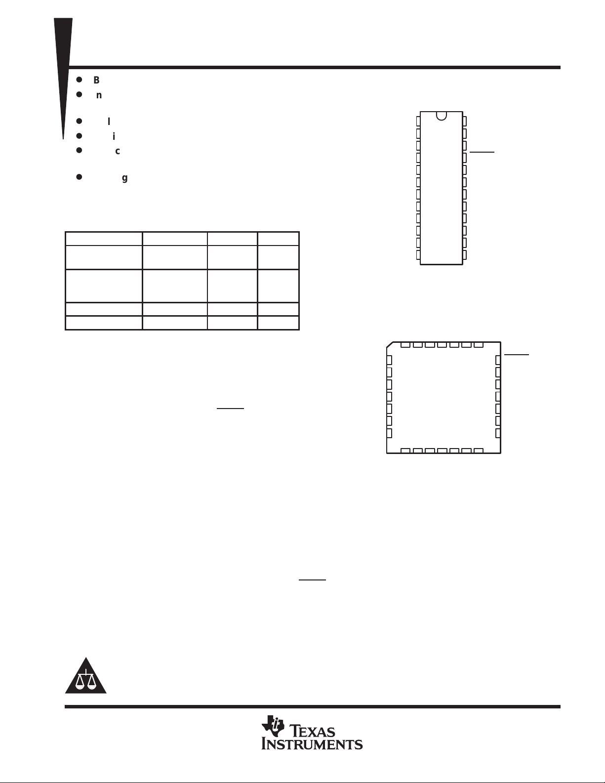
SN54ALS’, SN54AS’ . . . JT PACKAGE
SN74ALS’, SN74AS’ . . . DW OR NT PACKAGE
(TOP VIEW)
and B Buses
D
Multiplexed Real-Time and Stored Data
D
Choice of True or Inverting Data Paths
D
Choice of 3-State or Open-Collector
Outputs to A Bus
D
Package Options Include Plastic
Small-Outline (DW) Packages, Ceramic
Chip Carriers (FK), and Standard Plastic
(NT) and Ceramic (JT) 300-mil DIPs
DEVICE A OUTPUT B OUTPUT LOGIC
SN74ALS651A,
’AS651
SN54ALS652,
SN74ALS652A,
’AS652
’ALS653 Open Collector 3 State Inverting
SN74ALS654 Open Collector 3 State True
3 State 3 State Inverting
3 State 3 State True
description
These devices consist of bus-transceiver circuits,
D-type flip-flops, and control circuitry arranged for
multiplexed transmission of data directly from the
data bus or from the internal storage registers.
Output-enable (OEAB and OEBA
provided to control the transceiver functions.
Select-control (SAB and SBA) inputs are provided
to select real-time or stored data transfer. The
circuitry used for select control eliminates the
typical decoding glitch that occurs in a multiplexer
during the transition between stored and real-time
data. A low input level selects real-time data, and
) inputs are
CLKAB
OEAB
GND
SN54ALS’, SN54AS’ . . . FK PACKAGE
A1
A2
A3
NC
A4
A5
A6
SAB
A1
A2
A3
A4
A5
A6
A7
A8
4
5
6
7
8
9
10
11
12
A7
1
2
3
4
5
6
7
8
9
10
11
12
(TOP VIEW)
OEAB
SAB
CLKAB
321
13 14
A8
15 16 17
GND
NC – No internal connection
24
23
22
21
20
19
18
17
16
15
14
13
CC
NC
V
28 27 26
B8B7B6
NC
V
CC
CLKBA
SBA
OEBA
B1
B2
B3
B4
B5
B6
B7
B8
CLKBA
SAB
25
24
23
22
21
20
19
18
OEBA
B1
B2
NC
B3
B4
B5
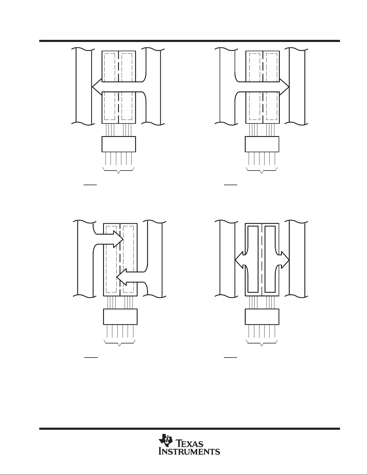
a high input level selects stored data. Figure 1
illustrates the four fundamental bus-management functions that can be performed with the octal bus
transceivers and registers.
Data on the A or B data bus, or both, can be stored in the internal D-type flip-flops by low-to-high transitions at
the appropriate clock (CLKAB or CLKBA) terminals, regardless of the select- or output-control terminals. When
SAB and SBA are in the real-time transfer mode, it is possible to store data without using the internal D-type
flip-flops by simultaneously enabling OEAB and OEBA
. In this configuration, each output reinforces its input.
When all other data sources to the two sets of bus lines are at high impedance, each set of bus lines remains
at its last state.
Please be aware that an important notice concerning availability, standard warranty, and use in critical applications of
Texas Instruments semiconductor products and disclaimers thereto appears at the end of this data sheet.
PRODUCTION DATA information is current as of publication date.
Products conform to specifications per the terms of Texas Instruments
standard warranty. Production processing does not necessarily include
testing of all parameters.
POST OFFICE BOX 655303 • DALLAS, TEXAS 75265
Copyright 1996, Texas Instruments Incorporated
1

SN54ALS652, SN54ALS653, SN54AS651, SN54AS652
SN74ALS651A, SN74ALS652A, SN74ALS653, SN74ALS654, SN74AS651, SN74AS652
OCTAL BUS TRANSCEIVERS AND REGISTERS WITH 3-STATE OUTPUTS
SDAS066F – DECEMBER 1983 – REVISED OCTOBER 1996
description (continued)
The -1 versions of the SN74ALS651A and SN74ALS652A are identical to the standard versions except that the
recommended maximum I
SN54ALS652, SN54ALS653, SN74ALS653, and SN74ALS654.
The SN54ALS’ and SN54AS’ families are characterized for operation over the full military temperature range
of –55°C to 125°C. The SN74ALS’ and SN74AS’ families are characterized for operation from 0°C to 70°C.
for the -1 versions is increased to 48 mA. There are no -1 versions of the
OL
2
POST OFFICE BOX 655303 • DALLAS, TEXAS 75265
SN54ALS652, SN54ALS653, SN54AS651, SN54AS652
SN74ALS651A, SN74ALS652A, SN74ALS653, SN74ALS654, SN74AS651, SN74AS652
OCTAL BUS TRANSCEIVERS AND REGISTERS WITH 3-STATE OUTPUTS
SDAS066F – DECEMBER 1983 – REVISED OCTOBER 1996
BUS A
3 21 1 23 2 22 1 23 2 22321
OEAB
OEBA
LL
CLKABXCLKBAXSABXSBA
REAL-TIME TRANSFER
BUS B TO BUS A
BUS A
BUS B
OEAB OEBA
L
BUS B
BUS A
HH
BUS A
BUS B
CLKABXCLKBAXSABLSBA
X
REAL-TIME TRANSFER
BUS A TO BUS B
BUS B
3 21 23 2 22 3 21 1 2 22
OEAB
Pin numbers are for the DW, JT, and NT packages.
OEBA
X
L
L
H
X
H
1
CLKAB CLKBAXSABXSBA
↑
XX
STORAGE FROM
A, B, OR A AND B
↑
↑↑
Figure 1. Bus-Management Functions
OEAB OEBA
X
X
X
POST OFFICE BOX 655303 • DALLAS, TEXAS 75265
X
H L H or L H H
23
CLKAB CLKBA SAB SBA
H or L
TRANSFER STORED DA TA
TO A AND/OR B
3
SN54ALS652, SN54ALS653, SN54AS651, SN54AS652
OPERATION OR FUNCTION
OPERATION OR FUNCTION
SN74ALS651A, SN74ALS652A, SN74ALS653, SN74ALS654, SN74AS651, SN74AS652
OCTAL BUS TRANSCEIVERS AND REGISTERS WITH 3-STATE OUTPUTS
SDAS066F – DECEMBER 1983 – REVISED OCTOBER 1996
FUNCTION TABLES
SN54ALS653, SN54AS651,
SN74ALS651A, SN74ALS653, SN74AS651
INPUTS
OEAB OEBA CLKAB CLKBA SAB SBA A1–A8 B1–B8
L H H or L H or L X X Input Input Isolation
L H ↑↑X X Input Input Store A and B data
X H ↑ H or L X X Input Unspecified
H H ↑↑X
L X H or L ↑ X X Unspecified
L L ↑↑XX
L L X X X L Output Input Real-time B data to A bus
L L X H or L X H Output Input Stored B data to A bus
H H X X L X Input Output Real-time A data to B bus
H H H or L X H X Input Output Stored A data to B bus
H L H or L H or L H H Output Output
†
The data output functions may be enabled or disabled by a variety of level combinations at OEAB or OEBA. Data input functions are always
enabled; i.e., data at the bus terminals is stored on every low-to-high transition on the clock inputs.
‡
Select control = L; clocks can occur simultaneously.
Select control = H; clocks must be staggered to load both registers.
‡
X Input Output Store A in both registers
‡
DATA I/O
‡
Output Input Store B in both registers
†
‡
Input Hold A, store B
Store A, hold B
Stored A data to B bus and
stored B
data to A bus
SN54ALS652, SN54AS652,
SN74ALS652A, SN74ALS654, SN74AS652
INPUTS
OEAB OEBA CLKAB CLKBA SAB SBA A1–A8 B1–B8
L H H or L H or L X X Input Input Isolation
L H ↑↑X X Input Input Store A and B data
X H ↑ H or L X X Input Unspecified
H H ↑↑X
L X H or L ↑ X X Unspecified
L L ↑↑XX
L L X X X L Output Input Real-time B data to A bus
L L X H or L X H Output Input Stored B data to A bus
H H X X L X Input Output Real-time A data to B bus
H H H or L X H X Input Output Stored A data to B bus
H L H or L H or L H H Output Output
†
The data output functions may be enabled or disabled by a variety of level combinations at OEAB or OEBA. Data input functions are always
enabled; i.e., data at the bus terminals is stored on every low-to-high transition on the clock inputs.
‡
Select control = L; clocks can occur simultaneously.
Select control = H; clocks must be staggered to load both registers.
‡
X Input Output Store A in both registers
‡
DATA I/O
‡
Output Input Store B in both registers
†
‡
Input Hold A, store B
Store A, hold B
Stored A data to B bus and
stored B data to A bus
4
POST OFFICE BOX 655303 • DALLAS, TEXAS 75265
SN54ALS652, SN54ALS653, SN54AS651, SN54AS652
SN74ALS651A, SN74ALS652A, SN74ALS653, SN74ALS654, SN74AS651, SN74AS652
OCTAL BUS TRANSCEIVERS AND REGISTERS WITH 3-STATE OUTPUTS
SDAS066F – DECEMBER 1983 – REVISED OCTOBER 1996
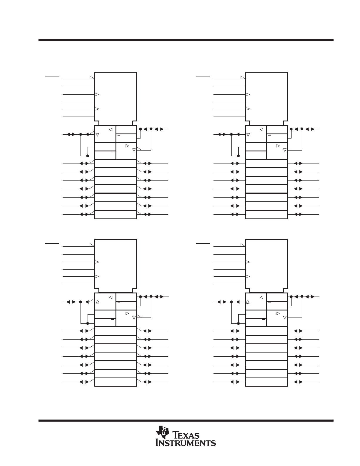
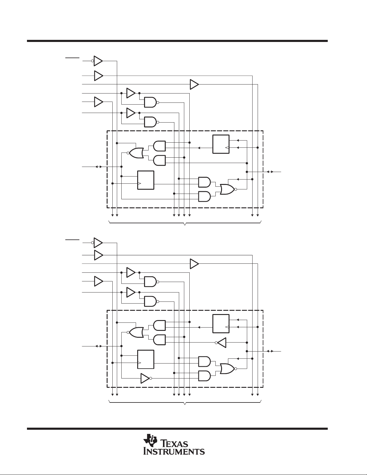
logic symbols
SBA
SAB
A1
A2
A3
A4
A5
A6
A7
A8
21
3
23
22
1
2
4
5
6
7
8
9
10
11
OEBA
OEAB
CLKBA
CLKAB
†
SN54AS651,
SN74ALS651A, SN74AS651
EN1 [BA]
EN2 [AB]
C4
G5
C6
G7
4D
5
≥1
1
6D ≥1
5
1
7
7
1
2
20
19
18
17
16
15
14
13
B1
B2
B3
B4
B5
B6
B7
B8
OEBA
OEAB
CLKBA
SBA
CLKAB
SAB
A1
A2
A3
A4
A5
A6
A7
A8
21
3
23
22
1
2
4
5
6
7
8
9
10
11
SN54ALS652, SN54AS652,
SN74ALS652A, SN74AS652
EN1 [BA]
EN2 [AB]
C4
G5
C6
G7
4D
5
≥1
1
6D ≥1
5
1
7
7
1
2
20
19
18
17
16
15
14
13
B1
B2
B3
B4
B5
B6
B7
B8
SN54ALS653, SN74ALS653 SN74ALS654
SBA
SAB
A1
A2
A3
A4
A5
A6
A7
A8
21
3
23
22
1
2
4
5
6
7
8
9
10
11
EN1 [BA]
EN2 [AB]
C4
G5
C6
G7
5
≥1
1
5
7
6D ≥1
7
1
20
19
18
17
16
15
14
13
B1
B2
B3
B4
B5
B6
B7
B8
4D
1
2
OEBA
OEAB
CLKBA
CLKAB
†
These symbols are in accordance with ANSI/IEEE Std 91-1984 and IEC Publication 617-12.
Pin numbers shown are for the DW, JT, and NT packages.
OEBA
OEAB
CLKBA
CLKAB
SBA
SAB
A1
A2
A3
A4
A5
A6
A7
A8
21
3
23
22
1
2
4
5
6
7
8
9
10
11
EN1 [BA]
EN2 [AB]
C4
G5
C6
G7
5
≥1
1
5
7
6D ≥1
7
1
20
19
18
17
16
15
14
13
B1
B2
B3
B4
B5
B6
B7
B8
4D
1
2
POST OFFICE BOX 655303 • DALLAS, TEXAS 75265
5
SN54ALS652, SN54ALS653, SN54AS651, SN54AS652
SN74ALS651A, SN74ALS652A, SN74ALS653, SN74ALS654, SN74AS651, SN74AS652
OCTAL BUS TRANSCEIVERS AND REGISTERS WITH 3-STATE OUTPUTS
SDAS066F – DECEMBER 1983 – REVISED OCTOBER 1996
logic diagrams (positive logic)
SBA
SAB
21
3
23
22
1
2
SN54ALS653, SN54AS651,
SN74ALS651A, SN74ALS653, SN74AS651
OEBA
OEAB
CLKBA
CLKAB
A1
OEBA
OEAB
CLKBA
SBA
CLKAB
SAB
4
21
3
23
22
1
2
One of Eight Channels
1D
C1
To Seven Other Channels
SN54ALS652, SN54AS652,
SN74ALS652A, SN74ALS654, SN74AS652
C1
1D
20
B1
One of Eight Channels
4
A1
1D
C1
Pin numbers shown are for the DW, JT, and NT packages.
6
POST OFFICE BOX 655303 • DALLAS, TEXAS 75265
To Seven Other Channels
C1
1D
20
B1
UNIT
IOLL
t
A
twPulse duration
ns
UNIT
IOLL
t
A
twPulse duration
ns
SN54ALS652, SN54ALS653, SN54AS651, SN54AS652
SN74ALS651A, SN74ALS652A, SN74ALS653, SN74ALS654, SN74AS651, SN74AS652
OCTAL BUS TRANSCEIVERS AND REGISTERS WITH 3-STATE OUTPUTS
SDAS066F – DECEMBER 1983 – REVISED OCTOBER 1996
absolute maximum ratings over operating free-air temperature range (unless otherwise noted)
Supply voltage, V
Input voltage, V
Operating free-air temperature range, T
Storage temperature range, T
†
Stresses beyond those listed under “absolute maximum ratings” may cause permanent damage to the device. These are stress ratings only, and
functional operation of the device at these or any other conditions beyond those indicated under “recommended operating conditions” is not
implied. Exposure to absolute-maximum-rated conditions for extended periods may affect device reliability.
7 V. . . . . . . . . . . . . . . . . . . . . . . . . . . . . . . . . . . . . . . . . . . . . . . . . . . . . . . . . . . . . . . . . . . . . . .
CC
: Control inputs 7 V. . . . . . . . . . . . . . . . . . . . . . . . . . . . . . . . . . . . . . . . . . . . . . . . . . . . . . . . . . . . . .
I
I/O ports 5.5 V. . . . . . . . . . . . . . . . . . . . . . . . . . . . . . . . . . . . . . . . . . . . . . . . . . . . . . . . . . . . . . . . .
: SN54ALS652 –55°C to 125°C. . . . . . . . . . . . . . . . . . . . . . . . . . . . . .
A
SN74ALS651A, SN74ALS652A 0°C to 70°C. . . . . . . . . . . . . . . . .
–65°C to 150°C. . . . . . . . . . . . . . . . . . . . . . . . . . . . . . . . . . . . . . . . . . . . . . . . . .
stg
recommended operating conditions
SN74ALS651A
MIN NOM MAX
V
CC
V
IH
V
IL
I
OH
f
clock
t
su
t
h
T
A
‡
Applies only to the SN74ALS651A-1 and only if VCC is maintained between 4.75 V and 5.25 V
Supply voltage 4.5 5 5.5 V
High-level input voltage 2 V
Low-level input voltage 0.8 V
High-level output current –15 mA
ow-level output curren
Clock frequency 0 40 MHz
CLKBA or CLKAB high 12.5
CLKBA or CLKAB low 12.5
Setup time before CLKAB↑ or CLKBA↑ A or B 10 ns
Hold time after CLKAB↑ or CLKBA↑ A or B 0 ns
Operating free-air temperature 0 70 °C
48
24
m
‡
†
recommended operating conditions
SN54ALS652 SN74ALS652A
MIN NOM MAX MIN NOM MAX
V
CC
V
IH
V
IL
I
OH
f
clock
t
su
t
h
T
A
‡
Applies only to the SN74ALS652A-1 and only if VCC is maintained between 4.75 V and 5.25 V
Supply voltage 4.5 5 5.5 4.5 5 5.5 V
High-level input voltage 2 2 V
Low-level input voltage 0.7 0.8 V
High-level output current –12 –15 mA
ow-level output curren
Clock frequency 0 35 0 40 MHz
CLKBA or CLKAB high 14.5 12.5
CLKBA or CLKAB low 14.5 12.5
Setup time before CLKAB↑ or CLKBA↑ A or B 15 10 ns
Hold time after CLKAB↑ or CLKBA↑ A or B 5 0 ns
Operating free-air temperature –55 125 0 70 °C
12 24
48
m
‡
POST OFFICE BOX 655303 • DALLAS, TEXAS 75265
7

SN54ALS652, SN54ALS653, SN54AS651, SN54AS652
PARAMETER
TEST CONDITIONS
UNIT
V
V
V
V
I
mA
I
V
V
V
A
I
V
5.5 V
V
0.4 V
A
SN74ALS651A, SN74ALS652A, SN74ALS653, SN74ALS654, SN74AS651, SN74AS652
OCTAL BUS TRANSCEIVERS AND REGISTERS WITH 3-STATE OUTPUTS
SDAS066F – DECEMBER 1983 – REVISED OCTOBER 1996
electrical characteristics over recommended operating free-air temperature range (unless
otherwise noted)
SN74ALS651A
MIN TYP†MAX
V
IK
V
OH
V
OL
I
IH
IL
I
O
I
CC
†
All typical values are at VCC = 5 V, TA = 25°C.
‡
For I/O ports, the parameters IIH and IIL include the off-state output current.
§
The output conditions have been chosen to produce a current that closely approximates one-half of the true short-circuit output current, IOS.
Control inputs VCC = 5.5 V, VI = 7 V 0.1
A or B ports VCC = 5.5 V, VI = 5.5 V 0.1
Control inputs
A or B ports
Control inputs
A or B ports
§
‡
‡
VCC = 4.5 V, II = –18 mA –1.2 V
VCC = 4.5 V to 5.5 V, IOH = –0.4 mA VCC–2
20
20
V
V
µ
m
mA
= 4.5
CC
= 4.5
CC
VCC = 4.75 V, IOL = 48 mA (-1 versions) 0.35 0.5
= 5.5 V,
CC
,
=
CC
VCC = 5.5 V, VO = 2.25 V –30 –112 mA
VCC = 5.5 V
IOH = –3 mA 2.4 3.2
IOH = –15 mA 2
IOL = 12 mA 0.25 0.4
IOL = 24 mA 0.35 0.5
= 2.7
I
=
I
Outputs high 42 68
Outputs low 52 82
Outputs disabled 52 82
–0.2
–0.2
8
POST OFFICE BOX 655303 • DALLAS, TEXAS 75265

PARAMETER
TEST CONDITIONS
UNIT
V
V
V
V
I
mA
I
V
5.5 V
V
2.7 V
A
I
V
V
V
A
SN54ALS652, SN54ALS653, SN54AS651, SN54AS652
SN74ALS651A, SN74ALS652A, SN74ALS653, SN74ALS654, SN74AS651, SN74AS652
OCTAL BUS TRANSCEIVERS AND REGISTERS WITH 3-STATE OUTPUTS
SDAS066F – DECEMBER 1983 – REVISED OCTOBER 1996
electrical characteristics over recommended operating free-air temperature range (unless
otherwise noted)
SN54ALS652 SN74ALS652A
MIN TYP†MAX MIN TYP†MAX
V
IK
OH
V
OL
Control inputs VCC = 5.5 V, VI = 7 V 0.1 0.1
I
A or B ports VCC = 5.5 V, VI = 5.5 V 0.1 0.1
Control inputs
IH
A or B ports
Control inputs
IL
A or B ports
§
I
O
I
CC
†
All typical values are at VCC = 5 V, TA = 25°C.
‡
For I/O ports, the parameters IIH and IIL include the off-state output current.
§
The output conditions have been chosen to produce a current that closely approximates one-half of the true short-circuit output current, IOS.
VCC = 4.5 V, II = –18 mA –1.2 –1.2 V
VCC = 4.5 V to 5.5 V, IOH = –0.4 mA VCC–2 VCC–2
IOH = –3 mA 2.4 3.2 2.4 3.2
VCC = 4.5 V
= 4.5
CC
VCC = 4.75 V, IOL = 48 mA (-1 versions) 0.35 0.5
,
=
CC
‡
= 5.5 V,
CC
‡
VCC = 5.5 V,
VCC = 5.5 V
IOH = –12 mA 2
IOH = –15 mA 2
IOL = 12 mA 0.25 0.4 0.25 0.4
IOL = 24 mA 0.35 0.5
=
I
= 0.4
I
VO = 2.25 V –20 –112 –30 –112 mA
Outputs high 47 76 47 76
Outputs low 55 88 55 88
Outputs disabled 55 88 55 88
20 20
20 20
–0.2 –0.2
–0.2 –0.2
V
µ
m
mA
POST OFFICE BOX 655303 • DALLAS, TEXAS 75265
9

SN54ALS652, SN54ALS653, SN54AS651, SN54AS652
CLKBA or CLKAB
A or B
ns
A or B
B or A
ns
‡
A or B
ns
‡
A or B
ns
OEBA
A
ns
OEBA
A
ns
OEAB
B
ns
OEAB
B
ns
SN74ALS651A, SN74ALS652A, SN74ALS653, SN74ALS654, SN74AS651, SN74AS652
OCTAL BUS TRANSCEIVERS AND REGISTERS WITH 3-STATE OUTPUTS
SDAS066F – DECEMBER 1983 – REVISED OCTOBER 1996
switching characteristics (see Figure 2)
VCC = 4.5 V to 5.5 V,
CL = 50 pF,
PARAMETER
f
max
t
PLH
t
PHL
t
PLH
t
PHL
t
PLH SBA or SAB
t
PHL
t
PLH SBA or SAB
t
PHL
t
PZH
t
PZL
t
PHZ
t
PLZ
t
PZH
t
PZL
t
PHZ
t
†
For conditions shown as MIN or MAX, use the appropriate value specified under recommended operating conditions.
‡
These parameters are measured with the internal output state of the storage register opposite that of the bus input.
PLZ
FROM
(INPUT)
(with A or B high)
(with A or B low)
TO
(OUTPUT)
R1 = 500 Ω,
R2 = 500 Ω,
TA = MIN to MAX
SN74ALS651A
MIN MAX
40 MHz
8 32
5 17
2 18
2 10
8 38
6 21
8 25
7 21
3 20
5 18
2 9
3 12
3 22
6 21
2 12
2 14
†
UNIT
10
POST OFFICE BOX 655303 • DALLAS, TEXAS 75265

CLKBA or CLKAB
A or B
ns
A or B
B or A
ns
‡
SBA or SAB
A or B
ns
‡
SBA or SAB
A or B
ns
OEBA
A
ns
OEBA
A
ns
OEAB
B
ns
OEAB
B
ns
SN54ALS652, SN54ALS653, SN54AS651, SN54AS652
SN74ALS651A, SN74ALS652A, SN74ALS653, SN74ALS654, SN74AS651, SN74AS652
OCTAL BUS TRANSCEIVERS AND REGISTERS WITH 3-STATE OUTPUTS
SDAS066F – DECEMBER 1983 – REVISED OCTOBER 1996
switching characteristics (see Figure 2)
VCC = 4.5 V to 5.5 V,
CL = 50 pF,
PARAMETER
f
max
t
PLH
t
PHL
t
PLH
t
PHL
t
PLH
t
PHL
t
PLH
t
PHL
t
PZH
t
PZL
t
PHZ
t
PLZ
t
PZH
t
PZL
t
PHZ
t
†
For conditions shown as MIN or MAX, use the appropriate value specified under recommended operating conditions.
‡
These parameters are measured with the internal output state of the storage register opposite that of the bus input.
PLZ
FROM
(INPUT)
SBA or SAB
(with A or B high)
SBA or SAB
(with A or B low)
TO
(OUTPUT)
R1 = 500 Ω,
R2 = 500 Ω,
TA = MIN to MAX
SN54ALS652 SN74ALS652A
MIN MAX MIN MAX
35 40 MHz
10 35 8 30
5 20 5 17
5 20 4 18
3 15 3 12
15 40 8 35
6 23 6 20
8 30 8 25
5 24 5 20
3 20 3 17
5 22 5 18
1 12 1 10
2 20 2 16
8 25 3 22
6 21 5 18
1 12 1 10
2 21 2 16
†
UNIT
POST OFFICE BOX 655303 • DALLAS, TEXAS 75265
11

SN54ALS652, SN54ALS653, SN54AS651, SN54AS652
UNIT
twPulse duration
ns
UNIT
twPulse duration
ns
SN74ALS651A, SN74ALS652A, SN74ALS653, SN74ALS654, SN74AS651, SN74AS652
OCTAL BUS TRANSCEIVERS AND REGISTERS WITH 3-STATE OUTPUTS
SDAS066F – DECEMBER 1983 – REVISED OCTOBER 1996
absolute maximum ratings over operating free-air temperature range (unless otherwise noted)
Supply voltage, V
Input voltage, V
Operating free-air temperature range, T
Storage temperature range, T
†
Stresses beyond those listed under “absolute maximum ratings” may cause permanent damage to the device. These are stress ratings only, and
functional operation of the device at these or any other conditions beyond those indicated under “recommended operating conditions” is not
implied. Exposure to absolute-maximum-rated conditions for extended periods may affect device reliability.
7 V. . . . . . . . . . . . . . . . . . . . . . . . . . . . . . . . . . . . . . . . . . . . . . . . . . . . . . . . . . . . . . . . . . . . . . .
CC
: All inputs and A I/O ports 7 V. . . . . . . . . . . . . . . . . . . . . . . . . . . . . . . . . . . . . . . . . . . . . . . . . . . .
I
B I/O ports 5.5 V. . . . . . . . . . . . . . . . . . . . . . . . . . . . . . . . . . . . . . . . . . . . . . . . . . . . . . . . . . . . . . .
: SN54ALS653 –55°C to 125°C. . . . . . . . . . . . . . . . . . . . . . . . . . . . . .
A
SN74ALS653, SN74ALS654 0°C to 70°C. . . . . . . . . . . . . . . . . . . .
–65°C to 150°C. . . . . . . . . . . . . . . . . . . . . . . . . . . . . . . . . . . . . . . . . . . . . . . . . .
stg
recommended operating conditions
SN54ALS653 SN74ALS653
MIN NOM MAX MIN NOM MAX
V
CC
V
IH
V
IL
V
OH
I
OH
I
OL
f
clock
t
su
t
h
T
A
Supply voltage 4.5 5 5.5 4.5 5 5.5 V
High-level input voltage 2 2 V
Low-level input voltage 0.7 0.8 V
High-level output voltage A ports 5.5 5.5 V
High-level output current B ports –12 –15 mA
Low-level output current 12 24 mA
Clock frequency 0 25 0 35 MHz
CLKBA or CLKAB high 20 14.5
CLKBA or CLKAB low 20 14.5
Setup time before CLKAB↑ or CLKBA↑ A or B 15 10 ns
Hold time after CLKAB↑ or CLKBA↑ A or B 5 0 ns
Operating free-air temperature –55 125 0 70 °C
†
recommended operating conditions
V
CC
V
IH
V
IL
V
OH
I
OH
I
OL
f
clock
t
su
t
h
T
A
Supply voltage 4.5 5 5.5 V
High-level input voltage 2 V
Low-level input voltage 0.8 V
High-level output voltage A ports 5.5 V
High-level output current B ports –15 mA
Low-level output current 24 mA
Clock frequency 0 35 MHz
Setup time before CLKAB↑ or CLKBA↑ A or B 10 ns
Hold time after CLKAB↑ or CLKBA↑ A or B 0 ns
Operating free-air temperature 0 70 °C
SN74ALS654
MIN NOM MAX
CLKBA or CLKAB high 14.5
CLKBA or CLKAB low 14.5
12
POST OFFICE BOX 655303 • DALLAS, TEXAS 75265

PARAMETER
TEST CONDITIONS
UNIT
VOHB ports
V
VOLV
V
V
I
mA
I
V
V
V
A
I
V
5.5 V
V
0.4 V
A
SN54ALS652, SN54ALS653, SN54AS651, SN54AS652
SN74ALS651A, SN74ALS652A, SN74ALS653, SN74ALS654, SN74AS651, SN74AS652
OCTAL BUS TRANSCEIVERS AND REGISTERS WITH 3-STATE OUTPUTS
SDAS066F – DECEMBER 1983 – REVISED OCTOBER 1996
electrical characteristics over recommended operating free-air temperature range (unless
otherwise noted)
SN54ALS653 SN74ALS653
MIN TYP†MAX MIN TYP†MAX
V
IK
p
Control inputs VCC = 5.5 V, VI = 7 V 0.1 0.1
I
A or B ports VCC = 5.5 V, VI = 5.5 V 0.1 0.1
Control inputs
IH
A or B ports
Control inputs
IL
A or B ports
I
A ports VCC = 4.5 V, VOH = 5.5 V 0.1 0.1 mA
OH
§
B ports VCC = 5.5 V, VO = 2.25 V –20 –112 –30 –112 mA
I
O
I
CC
†
All typical values are at VCC = 5 V, TA = 25°C.
‡
For I/O ports, the parameters IIH and IIL include the off-state output current.
§
The output conditions have been chosen to produce a current that closely approximates one-half of the true short-circuit output current, IOS.
VCC = 4.5 V, II = –18 mA –1.2 –1.2 V
VCC = 4.5 V to 5.5 V, IOH = –0.4 mA VCC–2 VCC–2
IOH = –3 mA 2.4 3.2 2.4 3.2
VCC = 4.5 V
‡
‡
VCC = 5.5 V
CC
CC
CC
= 4.5
= 5.5 V,
=
,
IOH = –12 mA 2
IOH = –15 mA 2
IOL = 12 mA 0.25 0.4 0.25 0.4
IOL = 24 mA 0.35 0.5
= 2.7
I
=
I
Outputs high 47 76 47 76
Outputs low 55 88 55 88
Outputs disabled 55 88 55 88
20 20
20 20
–0.2 –0.2
–0.2 –0.2
µ
m
mA
POST OFFICE BOX 655303 • DALLAS, TEXAS 75265
13

SN54ALS652, SN54ALS653, SN54AS651, SN54AS652
PARAMETER
TEST CONDITIONS
UNIT
V
V
V
V
V
V
I
mA
I
V
V
V
A
I
V
V
V
mA
SN74ALS651A, SN74ALS652A, SN74ALS653, SN74ALS654, SN74AS651, SN74AS652
OCTAL BUS TRANSCEIVERS AND REGISTERS WITH 3-STATE OUTPUTS
SDAS066F – DECEMBER 1983 – REVISED OCTOBER 1996
electrical characteristics over recommended operating free-air temperature range (unless
otherwise noted)
SN74ALS654
MIN TYP†MAX
V
IK
V
OH
OL
I
IH
IL
I
OH
I
O
I
CC
†
All typical values are at VCC = 5 V, TA = 25°C.
‡
For I/O ports, the parameters IIH and IIL include the off-state output current.
§
The output conditions have been chosen to produce a current that closely approximates one-half of the true short-circuit output current, IOS.
B ports
Control inputs VCC = 5.5 V, VI = 7 V 0.1
A or B ports VCC = 5.5 V, VI = 5.5 V 0.1
Control inputs
A or B ports
Control inputs
A or B ports
A ports VCC = 4.5 V, VOH = 5.5 V 0.1 mA
§
B ports VCC = 5.5 V, VO = 2.25 V –30 –112 mA
‡
‡
VCC = 4.5 V, II = –18 mA –1.2 V
VCC = 4.5 V to 5.5 V, IOH = –0.4 mA VCC–2
= 4.5
CC
= 4.5
CC
= 5.5 V,
CC
= 5.5 V,
CC
VCC = 5.5 V
IOH = –3 mA 2.4 3.2
IOH = –15 mA 2
IOL = 12 mA 0.25 0.4
IOL = 24 mA 0.35 0.5
= 2.7
I
= 0.4
I
Outputs high 47 76
Outputs low 55 88
Outputs disabled 55 88
20
20
–0.2
–0.2
µ
mA
V
14
POST OFFICE BOX 655303 • DALLAS, TEXAS 75265

CLKBA
A
ns
CLKAB
B
ns
A
B
ns
B
A
ns
‡
A
ns
‡
A
ns
‡
B
ns
‡
B
ns
OEBA
A
ns
OEAB
B
ns
OEAB
B
ns
SN54ALS652, SN54ALS653, SN54AS651, SN54AS652
SN74ALS651A, SN74ALS652A, SN74ALS653, SN74ALS654, SN74AS651, SN74AS652
OCTAL BUS TRANSCEIVERS AND REGISTERS WITH 3-STATE OUTPUTS
SDAS066F – DECEMBER 1983 – REVISED OCTOBER 1996
switching characteristics (see Figure 2)
VCC = 4.5 V to 5.5 V,
CL = 50 pF,
PARAMETER
f
max
t
PLH
t
PHL
t
PLH
t
PHL
t
PLH
t
PHL
t
PLH
t
PHL
t
PLH
t
PHL
t
PLH
t
PHL
t
PLH
t
PHL
t
PLH
t
PHL
t
PLH
t
PHL
t
PZH
t
PZL
t
PHZ
t
†
For conditions shown as MIN or MAX, use the appropriate value specified under recommended operating conditions.
‡
These parameters are measured with the internal output state of the storage register opposite that of the bus input.
PLZ
FROM
(INPUT)
SBA
(with B high)
SBA
(with B low)
SAB
(with A high)
SAB
(with A low)
TO
(OUTPUT)
RL = 680 Ω (A outputs),
R1 = R2 = 500 Ω (B outputs),
TA = MIN to MAX
SN54ALS653 SN74ALS653
MIN MAX MIN MAX
25 35 MHz
16 71 16 64
6 24 6 22
10 35 10 30
5 20 5 17
5 20 5 18
1.5 18 2 15
8 63 12 56
2 18 2 15
12 68 19 62
5 27 5 25
12 68 19 62
5 27 5 25
8 30 15 35
6 25 6 22
12 40 8 25
6 25 6 22
6 35 6 30
6 27 6 24
7 25 8 22
6 25 6 22
1 16 1 14
2 21 2 16
†
UNIT
POST OFFICE BOX 655303 • DALLAS, TEXAS 75265
15

SN54ALS652, SN54ALS653, SN54AS651, SN54AS652
CLKBA
A
ns
CLKAB
B
ns
A
B
ns
B
A
ns
‡
A
ns
‡
A
ns
‡
B
ns
‡
B
ns
OEBA
A
ns
OEAB
B
ns
OEAB
B
ns
SN74ALS651A, SN74ALS652A, SN74ALS653, SN74ALS654, SN74AS651, SN74AS652
OCTAL BUS TRANSCEIVERS AND REGISTERS WITH 3-STATE OUTPUTS
SDAS066F – DECEMBER 1983 – REVISED OCTOBER 1996
switching characteristics (see Figure 2)
VCC = 4.5 V to 5.5 V,
CL = 50 pF,
PARAMETER
f
max
t
PLH
t
PHL
t
PLH
t
PHL
t
PLH
t
PHL
t
PLH
t
PHL
t
PLH
t
PHL
t
PLH
t
PHL
t
PLH
t
PHL
t
PLH
t
PHL
t
PLH
t
PHL
t
PZH
t
PZL
t
PHZ
t
†
For conditions shown as MIN or MAX, use the appropriate value specified under recommended operating conditions.
‡
These parameters are measured with the internal output state of the storage register opposite that of the bus input.
PLZ
FROM
(INPUT)
SBA
(with B low)
SBA
(with B high)
SAB
(with A low)
SAB
(with A high)
TO
(OUTPUT)
RL = 680 Ω (A outputs),
R1 = R2 = 500 Ω (B outputs),
TA = MIN to MAX
SN74ALS654
MIN MAX
35 MHz
16 64
10 30
12 56
19 62
19 62
15 35
†
6 22
5 17
5 18
2 15
2 21
5 25
5 25
6 22
8 25
6 22
6 30
6 24
6 22
6 22
1 14
2 16
UNIT
16
POST OFFICE BOX 655303 • DALLAS, TEXAS 75265

tw*
Pulse duration
ns
SN54ALS652, SN54ALS653, SN54AS651, SN54AS652
SN74ALS651A, SN74ALS652A, SN74ALS653, SN74ALS654, SN74AS651, SN74AS652
OCTAL BUS TRANSCEIVERS AND REGISTERS WITH 3-STATE OUTPUTS
SDAS066F – DECEMBER 1983 – REVISED OCTOBER 1996
absolute maximum ratings over operating free-air temperature range (unless otherwise noted)
Supply voltage, V
Input voltage, V
Operating free-air temperature range, T
Storage temperature range, T
†
Stresses beyond those listed under “absolute maximum ratings” may cause permanent damage to the device. These are stress ratings only, and
functional operation of the device at these or any other conditions beyond those indicated under “recommended operating conditions” is not
implied. Exposure to absolute-maximum-rated conditions for extended periods may affect device reliability.
7 V. . . . . . . . . . . . . . . . . . . . . . . . . . . . . . . . . . . . . . . . . . . . . . . . . . . . . . . . . . . . . . . . . . . . . . .
CC
: Control inputs 7 V. . . . . . . . . . . . . . . . . . . . . . . . . . . . . . . . . . . . . . . . . . . . . . . . . . . . . . . . . . . . . .
I
I/O ports 5.5 V. . . . . . . . . . . . . . . . . . . . . . . . . . . . . . . . . . . . . . . . . . . . . . . . . . . . . . . . . . . . . . . . .
: SN54AS651, SN54AS652 –55°C to 125°C. . . . . . . . . . . . . . . . . . .
A
SN74AS651, SN74AS652 0°C to 70°C. . . . . . . . . . . . . . . . . . . . . .
–65°C to 150°C. . . . . . . . . . . . . . . . . . . . . . . . . . . . . . . . . . . . . . . . . . . . . . . . . .
stg
recommended operating conditions
SN54AS651
SN54AS652
MIN NOM MAX MIN NOM MAX
V
CC
V
IH
V
IL
I
OH
I
OL
f
clock
tsu* Setup time before CLKAB↑ or CLKBA↑ A or B 7 6 ns
th* Hold time after CLKAB↑ or CLKBA A or B 0 0 ns
T
A
* On products compliant to MIL-PRF-38535, this parameter is based on characterized data but is not production tested.
Supply voltage 4.5 5 5.5 4.5 5 5.5 V
High-level input voltage 2 2 V
Low-level input voltage 0.8 0.8 V
High-level output current –12 –15 mA
Low-level output current 32 48 mA
* Clock frequency 0 75 0 90 MHz
*
Operating free-air temperature –55 125 0 70 °C
CLKBA or CLKAB high 6 5
CLKBA or CLKAB low 7 6
SN74AS651
SN74AS652
UNIT
†
POST OFFICE BOX 655303 • DALLAS, TEXAS 75265
17

SN54ALS652, SN54ALS653, SN54AS651, SN54AS652
V
V
VOLV
4.5 V
V
I
mA
I
V
V
V
A
I
V
V
V
A
I
mA
SN74ALS651A, SN74ALS652A, SN74ALS653, SN74ALS654, SN74AS651, SN74AS652
OCTAL BUS TRANSCEIVERS AND REGISTERS WITH 3-STATE OUTPUTS
SDAS066F – DECEMBER 1983 – REVISED OCTOBER 1996
electrical characteristics over recommended operating free-air temperature range (unless
otherwise noted)
SN54AS651
PARAMETER TEST CONDITIONS
V
IK
OH
Control inputs VCC = 5.5 V, VI = 7 V 0.1 0.1
I
A or B ports VCC = 5.5 V, VI = 5.5 V 0.1 0.1
Control inputs
IH
A or B ports
Control input
IL
A or B ports
§
I
O
′AS651 VCC = 5.5 V
CC
′AS652 VCC = 5.5 V
†
All typical values are at VCC = 5 V, TA = 25 °C.
‡
For I/O ports, the parameters IIH and IIL include the off-state output current.
§
The output conditions have been chosen to produce a current that closely approximates one-half of the true short-circuit output current, IOS.
VCC = 4.5 V, II = –18 mA –1.2 –1.2 V
VCC = 4.5 V to 5.5 V, IOH = –2 mA VCC–2 VCC–2
IOH = –3 mA 2.4 3.2 2.4 3.2
VCC = 4.5 V
=
CC
= 5.5 V,
CC
‡
= 5.5 V,
CC
‡
VCC = 5.5 V, VO = 2.25 V –30 –112 –30 –112 mA
IOH = –12 mA 2
IOH = –15 mA 2
IOL = 32 mA 0.25 0.5
IOL = 48 mA 0.35 0.5
= 2.7
I
= 0.4
I
Outputs high 110 185 110 185
Outputs low 120 195 120 195
Outputs disabled 130 195 130 195
Outputs high 120 195 120 195
Outputs low 130 21 1 130 211
Outputs disabled 130 211 130 211
SN54AS652
MIN TYP†MAX MIN TYP†MAX
20 20
70 70
–0.5 –0.5
–0.75 –0.75
SN74AS651
SN74AS652
UNIT
µ
m
18
POST OFFICE BOX 655303 • DALLAS, TEXAS 75265

CLKBA or CLKAB
A or B
ns
A or B
B or A
ns
SBA
SAB
‡
A or B
ns
OEBA
A
ns
OEBA
A
ns
OEAB
B
ns
OEAB
B
ns
SN54ALS652, SN54ALS653, SN54AS651, SN54AS652
SN74ALS651A, SN74ALS652A, SN74ALS653, SN74ALS654, SN74AS651, SN74AS652
OCTAL BUS TRANSCEIVERS AND REGISTERS WITH 3-STATE OUTPUTS
SDAS066F – DECEMBER 1983 – REVISED OCTOBER 1996
switching characteristics (see Figure 2)
VCC = 4.5 V to 5.5 V,
CL = 50 pF,
PARAMETER
f
* 75 90 MHz
max
t
PLH
t
PHL
t
PLH
t
PHL
t
PLH
t
PHL
t
PZH
t
PZL
t
PHZ
t
PLZ
t
PZH
t
PZL
t
PHZ
t
PLZ
* On products compliant to MIL-PRF-38535, this parameter is based on characterized data but is not production tested.
†
For conditions shown as MIN or MAX, use the appropriate value specified under recommended operating conditions.
‡
These parameters are measured with the internal output state of the storage register opposite that of the bus input.
FROM
(INPUT)
or
TO
(OUTPUT)
R1 = 500 Ω,
R2 = 500 Ω,
TA = MIN to MAX
SN54AS651 SN74AS651
MIN MAX MIN MAX
2 11 2 8.5
2 10 2 9
2 12 2 8
1 8 1 7
2 15 2 11
2 11 2 9
2 11 2 10
3 18 3 16
2 10 2 9
2 10 2 9
3 12 3 11
3 20 3 16
2 11 2 10
2 12 2 11
†
UNIT
POST OFFICE BOX 655303 • DALLAS, TEXAS 75265
19

SN54ALS652, SN54ALS653, SN54AS651, SN54AS652
CLKBA or CLKAB
A or B
ns
A or B
B or A
ns
SBA
SAB
‡
A or B
ns
OEBA
A
ns
OEBA
A
ns
OEAB
B
ns
OEAB
B
ns
SN74ALS651A, SN74ALS652A, SN74ALS653, SN74ALS654, SN74AS651, SN74AS652
OCTAL BUS TRANSCEIVERS AND REGISTERS WITH 3-STATE OUTPUTS
SDAS066F – DECEMBER 1983 – REVISED OCTOBER 1996
switching characteristics (see Figure 2)
VCC = 4.5 V TO 5.5 V,
CL = 50 PF,
PARAMETER
f
* 75 90 MHz
max
t
PLH
t
PHL
t
PLH
t
PHL
t
PLH
t
PHL
t
PZH
t
PZL
t
PHZ
t
PLZ
t
PZH
t
PZL
t
PHZ
t
PLZ
* On products compliant to MIL-PRF-38535, this parameter is based on characterized data but is not production tested.
†
For conditions shown as MIN or MAX, use the appropriate value specified under recommended operating conditions.
‡
These parameters are measured with the internal output state of the storage register opposite that of the bus input.
FROM
(INPUT)
or
TO
(OUTPUT)
SN54AS652 SN74AS652
R1 = 500 Ω,
R2 = 500 Ω,
TA = MIN TO MAX
MIN MAX TYP MAX
2 11 2 8.5
2 10 2 9
2 12 2 9
1 8 1 7
2 15 2 11
2 11 2 9
2 11 2 10
3 18 3 16
2 10 2 9
2 10 2 9
3 12 3 11
3 20 3 16
2 11 2 10
2 12 2 11
†
UNIT
20
POST OFFICE BOX 655303 • DALLAS, TEXAS 75265

SN54ALS652, SN54ALS653, SN54AS651, SN54AS652
SN74ALS651A, SN74ALS652A, SN74ALS653, SN74ALS654, SN74AS651, SN74AS652
OCTAL BUS TRANSCEIVERS AND REGISTERS WITH 3-STATE OUTPUTS
SDAS066F – DECEMBER 1983 – REVISED OCTOBER 1996
PARAMETER MEASUREMENT INFORMATION
From Output
Under Test
CL = 50 pF
(see Note A)
Timing
Input
Data
Input
7 V
S1
LOAD CIRCUIT
FOR 3-STATE OUTPUTS
t
su
1.3 V
VOLTAGE WAVEFORMS
SETUP AND HOLD TIMES
Open
R1 = 500 Ω
1.3 V
Test Point
R2 = 500 Ω
t
h
1.3 V
3.5 V
0.3 V
3.5 V
0.3 V
SWITCH POSITION TABLE
TEST S1
t
PLH
t
PHL
t
PZH
t
PZL
t
PHZ
t
PLZ
Open
Open
Open
Closed
Open
Closed
High-Level
Pulse
Low-Level
Pulse
V
CC
R
L
From Output
Under Test
CL = 50 pF
(see Note A)
1.3 V
t
1.3 V
LOAD CIRCUIT
w
FOR OPEN-COLLECTOR OUTPUTS
VOLTAGE WAVEFORMS
PULSE DURATION
Test Point
1.3 V
1.3 V
3.5 V
0.3 V
3.5 V
0.3 V
Input
t
PLH
In-Phase
Output
t
PHL
Out-of-Phase
Output
NOTES: A. CL includes probe and jig capacitance.
B. Waveform 1 is for an output with internal conditions such that the output is low except when disabled by the output control.
Waveform 2 is for an output with internal conditions such that the output is high except when disabled by the output control.
C. All input pulses are supplied by generators having the following characteristics: PRR ≤ 1 MHz, Zo = 50 Ω, tr ≤ 2 ns, tf≤ 2 ns.
D. The outputs are measured one at a time with one transition per measurement.
1.3 V
1.3 V 1.3 V
VOLTAGE WAVEFORMS
PROPAGATION DELAY TIMES
1.3 V
Figure 2. Load Circuits and Voltage Waveforms
t
1.3 V1.3 V
t
PHL
PLH
3.5 V
0.3 V
V
OH
V
OL
V
OH
V
OL
Output
Control
Waveform 1
S1 Closed
(see Note B)
Waveform 2
S1 Open
(see Note B)
ENABLE AND DISABLE TIMES, 3-STATE OUTPUTS
t
PZL
t
PZH
1.3 V
1.3 V
t
PHZ
1.3 V
VOLTAGE WAVEFORMS
1.3 V
t
PLZ
V
0.3 V
3.5 V
0.3 V
3.5 V
OL
0.3 V
V
OH
0 V
POST OFFICE BOX 655303 • DALLAS, TEXAS 75265
21

IMPORTANT NOTICE
T exas Instruments and its subsidiaries (TI) reserve the right to make changes to their products or to discontinue
any product or service without notice, and advise customers to obtain the latest version of relevant information
to verify, before placing orders, that information being relied on is current and complete. All products are sold
subject to the terms and conditions of sale supplied at the time of order acknowledgement, including those
pertaining to warranty, patent infringement, and limitation of liability.
TI warrants performance of its semiconductor products to the specifications applicable at the time of sale in
accordance with TI’s standard warranty. Testing and other quality control techniques are utilized to the extent
TI deems necessary to support this warranty . Specific testing of all parameters of each device is not necessarily
performed, except those mandated by government requirements.
CERT AIN APPLICATIONS USING SEMICONDUCTOR PRODUCTS MAY INVOLVE POTENTIAL RISKS OF
DEATH, PERSONAL INJURY, OR SEVERE PROPERTY OR ENVIRONMENTAL DAMAGE (“CRITICAL
APPLICATIONS”). TI SEMICONDUCTOR PRODUCTS ARE NOT DESIGNED, AUTHORIZED, OR
WARRANTED TO BE SUITABLE FOR USE IN LIFE-SUPPORT DEVICES OR SYSTEMS OR OTHER
CRITICAL APPLICA TIONS. INCLUSION OF TI PRODUCTS IN SUCH APPLICATIONS IS UNDERST OOD TO
BE FULLY AT THE CUSTOMER’S RISK.
In order to minimize risks associated with the customer’s applications, adequate design and operating
safeguards must be provided by the customer to minimize inherent or procedural hazards.
TI assumes no liability for applications assistance or customer product design. TI does not warrant or represent
that any license, either express or implied, is granted under any patent right, copyright, mask work right, or other
intellectual property right of TI covering or relating to any combination, machine, or process in which such
semiconductor products or services might be or are used. TI’s publication of information regarding any third
party’s products or services does not constitute TI’s approval, warranty or endorsement thereof.
Copyright 1998, Texas Instruments Incorporated
 Loading...