

查询PTH03050Y供应商
PTHxx050Y —Series
6-A Non-Isolated DDR/QDR Memory
Bus Termination Modules
NOMINAL SIZE = 0.87 in x 0.5 in
(22,1 mm x 12,57 mm)
Description
The PTHxx050Y are a series of readyto-use switching regulator modules from
Texas Instruments designed specifically for
bus termination in DDR and QDR memory
applications. Operating from either a 3.3-V,
5-V or 12-V input, the modules generate
output that will source or sink up
a V
TT
to 6 A of current (8 A transient) to accurately track their V
required bus termination supply voltage,
and V
is the reference voltage for the
REF
memory and chipset bus receiver comparators. V
V
DDQ
REF
power supply voltage.
Both the PTHxx050Y series employs
an actively switched synchronous rectifier
input. VTT is the
REF
is usually set to half the
Features
• VTT Bus Termination Output
(Output Tracks the System V
• 6 A Output Current (8 A Peak)
• 3.3-V, 5-V or 12-V Input Voltage
• DDR & QDR Compatible
• On/Off Inhibit (for V
Standby)
TT
• Under-Voltage Lockout
• Operating Temp: –40 to +85 °C
output to provide state-of-the-art stepdown switching conversion. The products
are small in size (0.87 in × 0.5 in), and are
an ideal choice where space, performance,
and high efficiency are desired, along with
the convenience of a ready-to-use module.
Operating features include an on/off
inhibit and output over-current protection
(source mode only). The on/off inhibit
feature allows the V
bus to be turned
TT
off to save power in a standby mode of
operation.
Package options include both throughhole and surface mount configurations.
• Efficiencies up to 88 %
)
REF
• 50 W/in³ Power Density
• Output Over-Current Protection
• Safety Agency Approvals (Pending):
• Point-of-Load Alliance (POLA)
SLTS221 – MARCH 2004
(Non-Latching, Auto-Reset)
UL/cUL60950, EN60950, VDE
Compatible
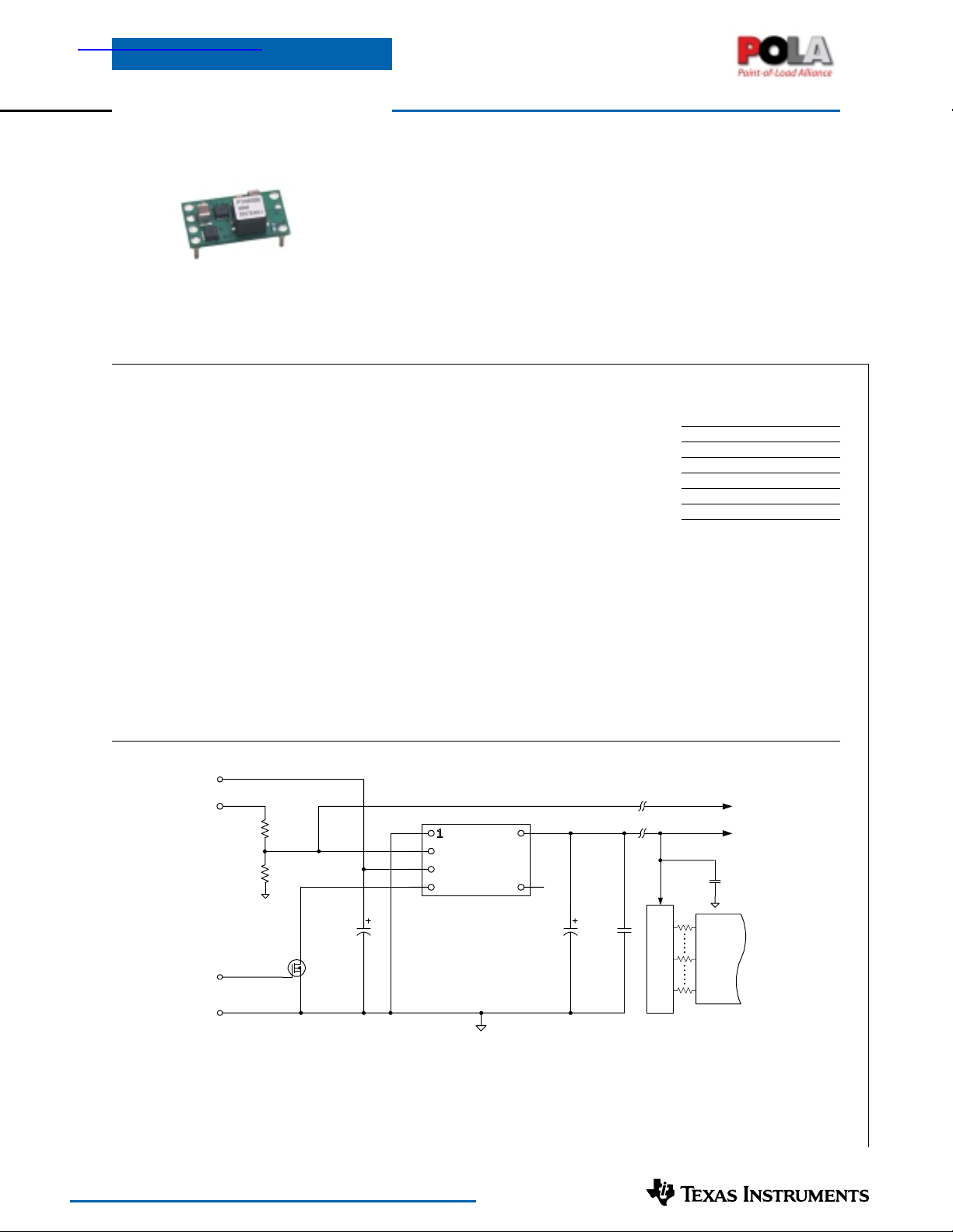
Pin Configuration
Pin Function
1 GND
2V
REF
3V
IN
4 Inhibit *
5 No Connect
6V
TT
* Denotes negative logic:
Open = VTT Output On
Ground = VTT Output Off
Standard Application
V
IN
V
DDQ
1 k
1 %
1 k
1 %
C
IN
(Required)
Q
1
Standby
GND
Cin= Required electrolytic capacitor; 220 µF (3.3-/5-V input), 560 µF (12-V input).
Co1= Required low-ESR electrolyitic capacitor; 470 µF (3.3-/5-V input), 940 µF (12-V input).
Co2= Ceramic capacitance for optimum response to a 3-A (±1.5-A) load transient.; 200 µF (3.3-/5-V input), 400 µF (12-V input).
Con= Distributed hf-ceramic decoupling capacitors for VTT bus; as recommended for DDR memory appications.
BSS138
(Optional)
1
2
3
4
PTHxx050Y
(Top View)
6
5
Co
1
Low-ESR
(Required)
Co
2
Ceramic
(Optional)
Co
n
hf-Ceramic
V
TT
Termination Island
SSTL-2
Data/
Address
Bus
V
REF
V
TT
For technical support and further information, visit http://power.ti.com
PTHxx050Y —Series
6-A Non-Isolated DDR/QDR Memory
Bus Termination Modules
Ordering Information
Input Voltage
(PTHHH050Yxx)
Code Input Voltage
03 3.3 V
05 5 V
12 12 V
Notes: (1) Add “T” to end of part number for tape and reel on SMD packages only.
(2) Reference the applicable package reference drawing for the dimensions and PC board layout
(3) “Standard” option specifies 63/37, Sn/Pb pin solder material.
Package Options
(PTHxx050YHH)
Code Description Pkg Ref.
AH Horiz. T/H (EUU)
AS SMD, Standard
Pin Descriptions
VIN: The positive input voltage power node to the mod-
ule, which is referenced to common GND.
GND: This is the common ground connection for the
V
and VTT power connections. It is also the 0-VDC
IN
reference for the control inputs.
V
: The module senses the voltage at this input to regu-
REF
late the output voltage, VTT. The voltage at V
the reference voltage for the system bus receiver comparators. It is normally set to precisely half the bus driver
supply voltage (V
÷ 2), using a resistor divider (see
DDQ
standard application). The Thevenin impedance of the
network driving the V
pin should not exceed 500 Ω.
REF
REF
is also
SLTS221 – MARCH 2004
(1)
(2)
(3)
(EUV)
VTT: This is the regulated power output from the module
with respect to the GND node, and the tracking termination supply for the application data and address buses.
It is precisely regulated to the voltage applied to the
module’s V
input, and is active active about 20 ms
REF
after a valid input source is applied to the module. Once
active it will track the voltage applied at V
REF
.
Inhibit: The Inhibit pin is an open-collector/drain negative
logic input that is referenced to GND. Applying a lowlevel ground signal to this input turns off the output
voltage, VTT. When the Inhibit is active, the input current drawn by the regulator is significantly reduced. If
the Inhibit pin is left open circuit, the module will produce an output whenever a valid input source is applied.
Environmental & Absolute Maximum Ratings (Voltages are with respect to GND)
Characteristics Symbols Conditions Min Typ Max Units
Control Input Voltage V
Operating Temperature Range T
Solder Reflow Temperature T
Storage Temperature T
Mechanical Shock Per Mil-STD-883D, Method 2002.3
Mechanical Vibration Mil-STD-883D, Method 2007.2
Weight — — 2.9 — grams
Flammability — Meets UL 94V-O
Notes: (i) For operation below 0 °C the external capacitors m ust bave stable characteristics. use either a low ESR tantalum, Os-Con, or ceramic capacitor.
(ii) During reflow of SMD package version do not elevate peak temperature of the module, pins or internal components above the stated maximum.
REF
a
reflow
s
Over Vin Range –40
Surface temperature of module body or pins 235
— –40 — 125 °C
1 msec, ½ Sine, mounted
20-2000 Hz
–0.3 — Vin + 0.3 V
(i)
— 85 °C
— 500 — G’s
—20— G’s
For technical support and further information, visit http://power.ti.com
(ii)
°C
PTHxx050Y —Series
6-A Non-Isolated DDR/QDR Memory
Bus Termination Modules
Specifications (Unless otherwise stated, T
=25 °C; nominal Vin; V
a
=1.25 V; Cin, Co1, & Co2 =typical values; and Io =Iomax)
REF
SLTS221 – MARCH 2004
PTHxx050Y
Characteristics Symbols Conditions Min Typ Max Units
Output Current I
Input Voltage Range V
Tracking Range for V
Tracking Tolerance to V
REF
REF
∆V
V
o
in
REF
–V
Over line, load and temperature –10 — +10 mV
TT
REF
Efficiency η I
Vo Ripple (pk-pk) V
r
Over ∆V
range, Continuous 0 — ±6
REF
Repetitive pulse — — ±8
Over Io range PTH03050Y 2.95 — 3.65
PTH05050Y 4.5 — 5.5 V
PTH12050Y 10.8 — 13.2
0.55 — 1.8 V
=4 A PTH03050Y — 88 —
o
PTH05050Y — 87 — %
PTH12050Y — 84 —
20 MHz bandwidth — 20 — mVpp
(1)
(2)
Over-Current Threshold Io trip Reset, followed by auto-recovery — 12 — A
Load Transient Response 15 A/µs load step, fr om –1.5 A to +1.5 A
t
∆V
tr
tr
Under-Voltage Lockout UVLO V
Inhibit Control (pin4) Referenced to GND
Input High Voltage V
Input Low Voltage V
IH
IL
(See note 5) Recovery Time — 80 — µSec
increasing PTH03050Y — 2.45 2.8
in
decreasing PTH03050Y 2.2 2.40 —
V
in
Vo over/undershoot — 25 40 mV
PTH05050Y — 4.3 4.45 V
PTH12050Y — 9.5 10.4
PTH05050Y 3.4 3.7 — V
PTH12050Y 8.8 9 —
Vin –0.5 — Open
–0.2 — 0.6
(3)
Input Low Current IIL inhibit Pin to GND — –130 — µA
Input Standby Current Iin inh Inhibit (pin 4) to GND — 10 — mA
Switching Frequency ƒ
External Input Capacitance C
External Output Capacitance Co
s
in
, Co
1
Reliability MTBF Per Bellcore TR-332 6 — — 10
Notes:
(1) Rating is conditional on the module being directly soldered to a 4-layer PCB with 1 oz. copper. See the SOA curves or contact the factory for appropriate
derating. The PTH03050Y and PTH05050Y require no derating up to 85 °C operating temperature and natural convection airflow.
(2) Up to 10 ms pulse period at 10 % maximum duty.
(3) This control pin has an internal pull-up to the input voltage Vin. If it is left open-circuit the module will operate when input power is applied. A small
low-leakage (<100 nA) MOSFET is recommended for control. For further information, consult the related application note.
(4) An input capacitor is required for proper operation. The capacitor must be rated for a minimum of 300 mA rms (750 mA rms for 12-V input) of ripple
current.
(5) The typical value of external output capacitance value ensures that V
terminations. Lower values of capacitance may be possible when the
(6) This is the calculated maximum. The minimum ESR limitation will often result in a lower value. Consult the application notes for further guidance.
(7) This is the typcial ESR for all the electrolytic (non-ceramic) output capacitance. Use 7 m
Over Vin & Io ranges PTH03050Y/PTH05050Y 550 600 650
PTH03050Y/PTH05050Y 220
Capacitance value:
2
non-ceramic PTH03050Y/PTH05050Y 0 470
ceramic PTH03050Y/PTH05050Y 0 200
Equiv. series resistance (non-ceramic) 4
PTH12050Y 200 250 300
(4)
PTH12050Y 560
(4)
PTH12050Y — 940
PTH12050Y 0 400
(7)
50 % stress, Ta =40 °C, ground benign
meets the specified transient performance requirements for the memory bus
TT
measured peak change in output current is consistently less than 3 A.
Ω
as the minimum when using max-ESR values to calculate.
——
——
(5)
(5)
(5)
(5)
(6)
3,300
(6)
3,300
300 µF
600
——mΩ
A
A
V
kHz
µF
µF
6
Hrs
For technical support and further information, visit http://power.ti.com

PTHxx050Y —Series
)
)
Typical Characteristics
6-A Non-Isolated DDR/QDR Memory
Bus Termination Modules
Characteristic Data; V
Efficiency vs Load Current
100
90
80
70
Efficiency - %
60
50
0123456
Output Ripple vs Load Current (See Note 2 to Table)
50
40
30
20
Ripple - mV
10
0
0123456
Iout - Amps
Iout - Amps
=1.25 V (See Note A)
REF
V
IN
3.3 V
5 V
12 V
V
IN
3.3 V
5 V
12 V
Safe Operating Area; V
PTH03050Y/PTH05050Y at nominal V
90
80
70
60
50
40
Ambient Temperature (°C)
30
20
0123456
PTH12050Y only; VIN =12 V
90
80
70
60
50
40
Ambient Temperature (°C)
30
20
0123456
Iout (A
Iout (A
=1.25 V (See Note B)
REF
SLTS221 – MARCH 2004
IN
Airflow
Nat Conv
Airflow
400LFM
200LFM
100LFM
Nat Conv
Power Dissipation vs Load Current
1.5
1.2
0.9
0.6
Pd - Watts
0.3
0
0123456
Iout - Amps
V
IN
3.3 V
5 V
12 V
Transient Performance for
∆∆
∆4-A Load Change
∆∆
PTH03050Y: Sink to Source Transient
HORIZ SCALE: 100 µs/Div
V – V
TT
(50 mV/Div)
(5 A/Div)
±I
TT
REF
Note A: Characteristic data has been developed from actual products tested at 25°C. This data is considered typical data for the Converter.
Note B:
SOA graphs represent the conditions at which internal components are at or below the manufacturer’s maximum operating temperatures. Derating limits apply to
modules soldered directly to a 4 in
×
4 in. double-sided PCB with 1 oz. copper.
For technical support and further information, visit http://power.ti.com


IMPORTANT NOTICE
Texas Instruments Incorporated and its subsidiaries (TI) reserve the right to make corrections, modifications,
enhancements, improvements, and other changes to its products and services at any time and to discontinue
any product or service without notice. Customers should obtain the latest relevant information before placing
orders and should verify that such information is current and complete. All products are sold subject to TI’s terms
and conditions of sale supplied at the time of order acknowledgment.
TI warrants performance of its hardware products to the specifications applicable at the time of sale in
accordance with TI’s standard warranty. Testing and other quality control techniques are used to the extent TI
deems necessary to support this warranty . Except where mandated by government requirements, testing of all
parameters of each product is not necessarily performed.
TI assumes no liability for applications assistance or customer product design. Customers are responsible for
their products and applications using TI components. To minimize the risks associated with customer products
and applications, customers should provide adequate design and operating safeguards.
TI does not warrant or represent that any license, either express or implied, is granted under any TI patent right,
copyright, mask work right, or other TI intellectual property right relating to any combination, machine, or process
in which TI products or services are used. Information published by TI regarding third-party products or services
does not constitute a license from TI to use such products or services or a warranty or endorsement thereof.
Use of such information may require a license from a third party under the patents or other intellectual property
of the third party, or a license from TI under the patents or other intellectual property of TI.
Reproduction of information in TI data books or data sheets is permissible only if reproduction is without
alteration and is accompanied by all associated warranties, conditions, limitations, and notices. Reproduction
of this information with alteration is an unfair and deceptive business practice. TI is not responsible or liable for
such altered documentation.
Resale of TI products or services with statements different from or beyond the parameters stated by TI for that
product or service voids all express and any implied warranties for the associated TI product or service and
is an unfair and deceptive business practice. TI is not responsible or liable for any such statements.
Following are URLs where you can obtain information on other Texas Instruments products and application
solutions:
Products Applications
Amplifiers amplifier.ti.com Audio www.ti.com/audio
Data Converters dataconverter.ti.com Automotive www.ti.com/automotive
DSP dsp.ti.com Broadband www.ti.com/broadband
Interface interface.ti.com Digital Control www.ti.com/digitalcontrol
Logic logic.ti.com Military www.ti.com/military
Power Mgmt power.ti.com Optical Networking www.ti.com/opticalnetwork
Microcontrollers microcontroller.ti.com Security www.ti.com/security
Telephony www.ti.com/telephony
Video & Imaging www.ti.com/video
Wireless www.ti.com/wireless
Mailing Address: Texas Instruments
Post Office Box 655303 Dallas, Texas 75265
Copyright 2004, Texas Instruments Incorporated

Copyright © Each Manufacturing Company.
All Datasheets cannot be modified without permission.
This datasheet has been download from :
www.AllDataSheet.com
100% Free DataSheet Search Site.
Free Download.
No Register.
Fast Search System.
www.AllDataSheet.com
 Loading...