

查询PT6510供应商
PT6510 Series
8-A 5-V/3.3-V Input Adjustable ISR
with Short-Circuit protection
Description
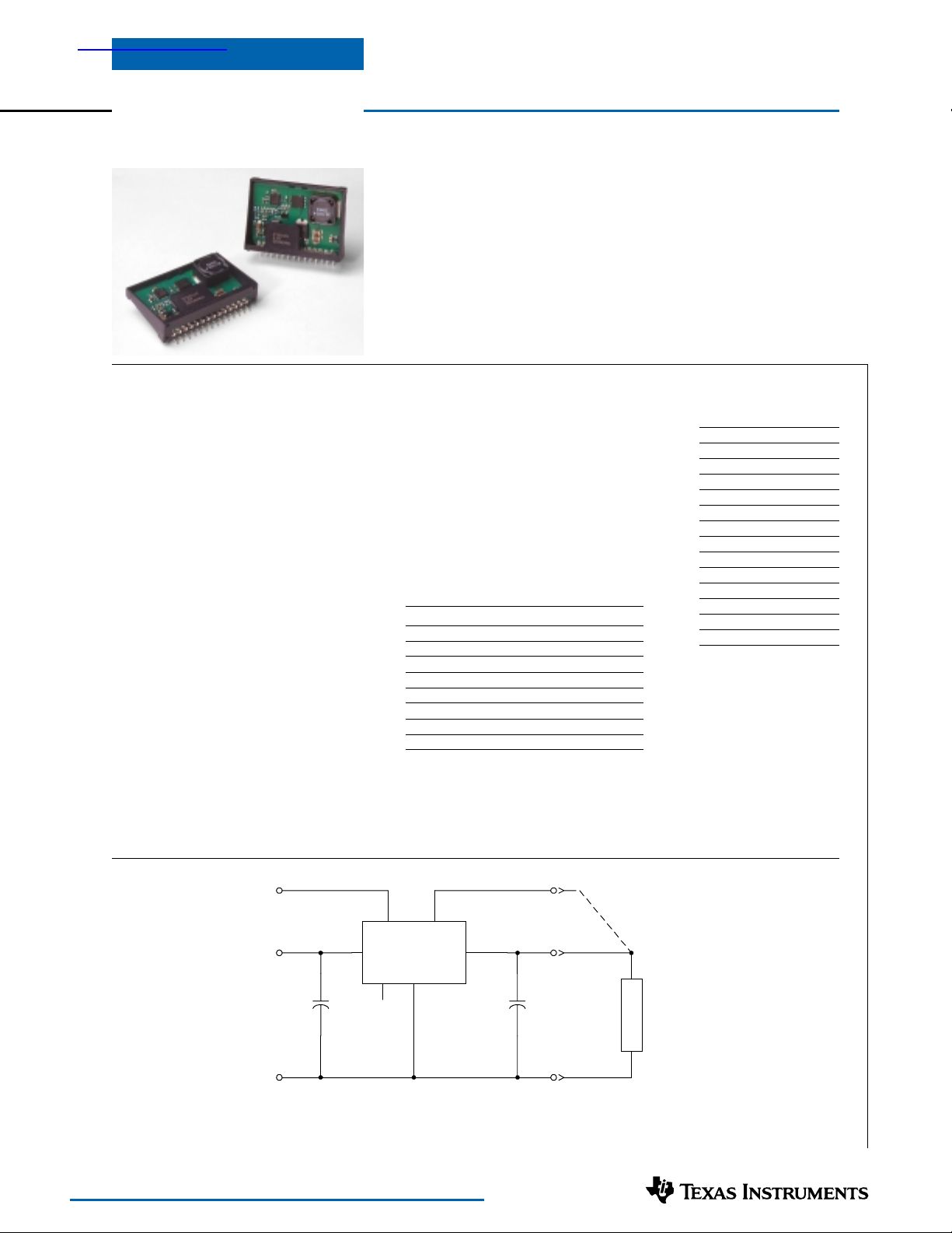
The PT6510 series of power modules
is the recommended direct replacement
for the PT6500 series in existing designs.
The modules have the same output current rating as the PT6500 series (8 A)
and were designed to be functionally identical in as many aspects as possible. This
includes the input voltage range, on/off
standby control, and output voltage adjustment.
When used as a replacement, a PT6510
series part exhibits a number of performance enhancements over its PT6500
series equivalent. These include improved
power dissipation and efficiency, significantly reduced inrush current, and better
line and load regulation.
The modules are housed in the same
14-Pin SIP (Single In-line Package), and
include the same package options.
Features
• 8-A Rated Output Current
• Replaces PT6500 Series
• High Efficiency (91% for PT6511)
• Small Footprint (0.75 in², Suffix ‘N’)
• Output On/Off Standby Control
• Output Short-Circuit Protection
• Over-Temperature Protection
• Adjustable Output Voltage
• Soft Startup
• 16-pin Mount Option (Suffixes L & F)
Ordering Information
PT6511¨ = 3.3 Volts
† PT6512¨ = 1.5 Volts
PT6513¨ = 2.5 Volts
PT6514¨ = 3.6 Volts
† PT6515¨ = 1.2 Volts
† PT6516¨ = 1.8 Volts
† 3.3V Input Bus Capable
PT Series Suffix
Case/Pin Order Package
Configuration Suffix Code *
Vertical N (EED)
Horizontal A (EEA)
SMD C (EEC)
Horizontal, Top Tab H (EEH)
SMD, 2-Pin Tab L (EEL)
SMD, 2-Pin Ext Tab F (EEF)
Vertical, Side Tab R (EEE)
Horizontal, Side Tab G (EEG)
SMD, Side Tab B (EEK)
* Previously known as package styles 400/410.
(Package availability varies with output voltage option.
Reference the applicable package code drawing for the
dimensions and PC board layout)
(PT1234x)
SLTS220 FEBRUARY 2004
Pin-Out Information
Pin Function
1Vo Sense
2 Do Not Connect
3 STBY*
4V
in
5V
in
6V
in
7 GND
8 GND
9 GND
10 GND
11 V
out
12 V
out
13 V
out
14 V
* For further information, see
application notes.
out
Adjust
Standard Application
VoADJ
V
IN
C
COM
For technical support or further information, visit http://power.ti.com
4,5,6
+
IN
14
PT6510
7–10
3
SENSE
V
o
1
V
11,12,13
C
OUT
OUT
+
COM
L
O
A
D
Cin= Required 330 µF electrolytic capacitor.
C
= Required 330 µF electrolytic capacitor.
out
PT6510 Series
8-A 5-V/3.3-V Input Adjustable ISR
with Short-Circuit protection
Specifications (Unless otherwise stated, T
=25 °C, Vin =5 V, Cin =330 µF, C
a
=330 µF, and Io =Iomax)
out
SLTS220 FEBRUARY 2004
PT6510 SERIES
Characteristic Symbol Conditions Min Typ Max Units
Output Current I
Input Voltage Range V
o
in
Over Vin range 0.1
Over Io Range V
≥ 2.5 V 4.5
o
≤ 1.8 V 3.1
V
o
Vo = 3.6 V 4.8
(1)
—8 A
(2)
—6
(2)
— 6 VDC
(2)
—6
Output Voltage Tolerance Vo tol Ta = –40 to +85 °C Vo – 0.1 — Vo + 0. 1 V
Line Regulation Reg
Load Regulation Reg
line
load
Efficiency η I
Vo Ripple (pk-pk) V
r
Over Vin range ±2 — ±10 mV
Over Io range ±2 — ±10 mV
=3 A Vo =3.3 V — 92 —
o
=8 A Vo =3.3 V — 91 —
I
o
Vo =2.5 V — 89 —
=1.8 V — 83 — %
V
o
=1.5 V — 80 —
V
o
Vo =1.2 V — 75 —
=2.5 V — 87 —
V
o
Vo =1.8 V — 81 — %
=1.5 V — 77 —
V
o
Vo =1.2 V — 72 —
20 MHz bandwidth — 15 — mV
Over-Current Threshold Io trip Reset, followed by auto-recovery — 15 — A
Transient Response t
Switching Frequency ƒ
On/Off Standby (Pin 3) Referenced to –Vin (pin 7)
Input High Voltage V
Input Low Voltage V
Input Low Current I
∆V
tr
tr
s
IH
IL
IL
1 A/µs load step, 50 % to 100 % Iomax — 100 — µs
Vo over/undershoot — ±150 — mV
Over Vin and Io range 475 550 725 kHz
— — Open
–0.1 — +0.4
(3)
— –0.5 – mA
Standby Input Current Iin stby Pins 3 & 7 connected — 1 5 mA
External Output Capacitance C
External Input Capacitance C
Operating Temperature Range T
Storage Temperature T
out
in
a
s
Reliability MTBF Per Bellcore TR-332
Mechanical Shock — Per Mil-Std-883D, method 2002.3,
Mechanical Vibration — Per Mil-Std-883D, method 2007.2,
Weight — Suffixes N, A, & C — 12.5 —
See application schematic 330 — 5,000
See application schematic 330
(5)
——µF
Over Vin range –40 — +85
— –40 — +125 °C
50 % stress, Ta =40 °C, ground benign
1 ms, half-sine, mounted to a fixture
20-2000 Hz
Suffixes R, G & B — 16.5 —
Suffix H — 18.5 — grams
Suffix L — 15.5 —
Suffix F — 22 —
6.4 — — 10
— 500 — G’s
—10—G’s
(4)
(6)
Flammability — Materials meet UL 94V-0
Notes: (1) The ISR will operate at no load with reduced specifications.
(2) The minimum input voltage required by the part is V
(3) The STBY* control (pin 3) has an internal pull-up and if it is left open circuit the module will operate when input power is applied. The open-circuit
voltage is the input voltage, Vin. Refer to the application notes for other interface considerations.
(4) The module requires a 330 µF output capacitor for proper operation in all applications. For transient or dynamic load applications, additional output
capacitance (Cout) may be necessary. The maximum allowable output capacitance is 5,000 µF.
(5) In addition, the input capacitance (C
application note on capacitor recommendations.
(6) See Safe Operating Area curves or contact the factory for the appropriate derating.
) must be rated for a minimum of 1.2 Arms ripple current rating. For more information consult the related
in
+ 1.2 V, or 3.1 V, whichever is greater.
out
(7) The tab pins on the 16-pin mount package types (suffix L) must be soldered. For more information see the applicable package outline drawing.
pp
V
µF
°C
6
Hrs
For technical support and further information, visit http://power.ti.com
PT6510 Series
)
)
)
)
)
)
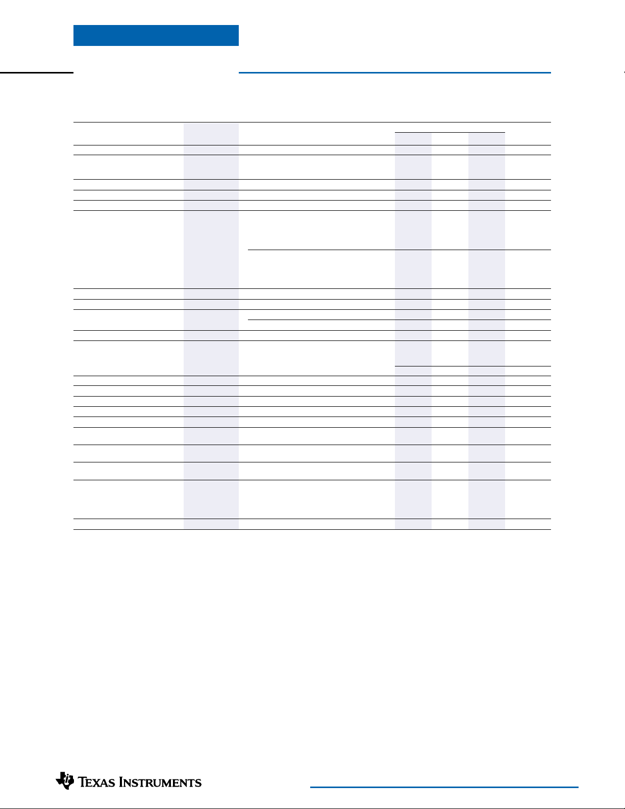
Typical Characteristics
8-A 5-V/3.3-V Input Adjustable ISR
with Short-Circuit protection
Characteristic Data; Vin =5 V (See Note A) Characteristic Data; Vin =3.3 V (See Note A)
Efficiency vs Output Current Efficiency vs Output Current
100
90
80
70
Efficiency - (%)
60
50
02468
Output Ripple vs Output Current
40
30
20
Ripple Voltage - (mV)
10
I
- (A
OUT
V
OUT
3.6 V
3.3 V
2.5 V
1.8 V
1.5 V
1.2 V
V
OUT
1.8 V
2.5 V
3.3 V
1.5 V
3.6 V
1.2 V
100
90
80
70
Efficiency - (%)
60
50
02468
Output Ripple vs Output Current
40
30
20
Ripple Voltage - (mV)
10
I
- (A
OUT
SLTS220 FEBRUARY 2004
V
OUT
2.5 V
1.8 V
1.5 V
1.2 V
V
OUT
1.8 V
1.5 V
1.2 V
2.5 V
0
02468
Power Dissipation vs Output Current Power Dissipation Output Current
4
3
2
1
Power Dissipation - (W)
0
02468
I
- (A
OUT
V
OUT
1.2 V
1.5 V
1.8 V
2.5 V
3.3 V
3.6 V
I
- (A
OUT
0
02468
4
3
2
1
Power Dissipation - (W)
0
02468
I
- (A
OUT
I
- (A
OUT
V
OUT
1.2 V
1.5 V
1.8 V
2.5 V
Note A: Characteristic data has been developed from actual products tested at 25°C. This data is considered typical data for the Converter.
For technical support or further information, visit http://power.ti.com
)
)
)
PT6510 Series
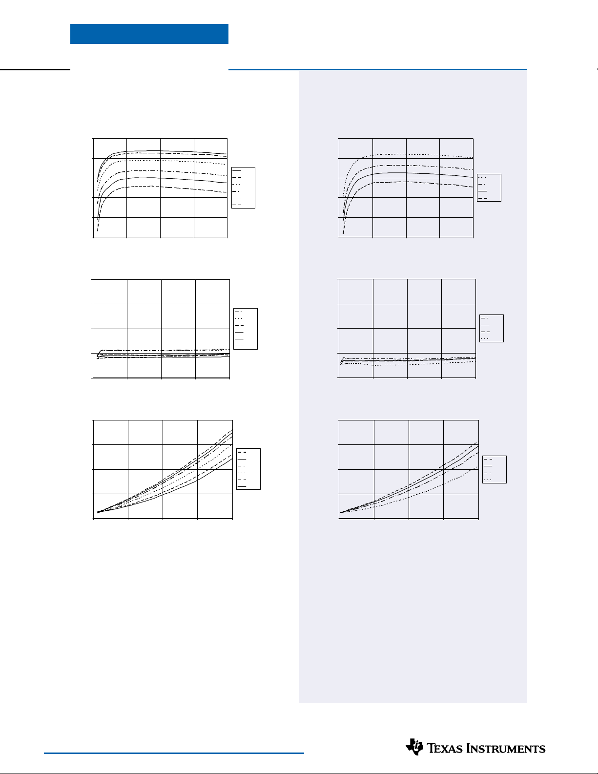
Typical Characteristics
8-A 5-V/3.3-V Input Adjustable ISR
with Short-Circuit protection
in
PT6511; V
90
80
70
60
50
40
Ambient Temperature (°C)
30
20
012345678
PT6515; V
90
80
70
60
50
40
Ambient Temperature (°C)
30
20
012345678
= 3.3 V PT6515; V
OUT
I
(A
OUT
= 1.2 V
OUT
I
(A
OUT
=5 V (See Note B)
Airflow
200LFM
120LFM
60LFM
Nat Conv
Airflow
200LFM
120LFM
60LFM
Nat Conv
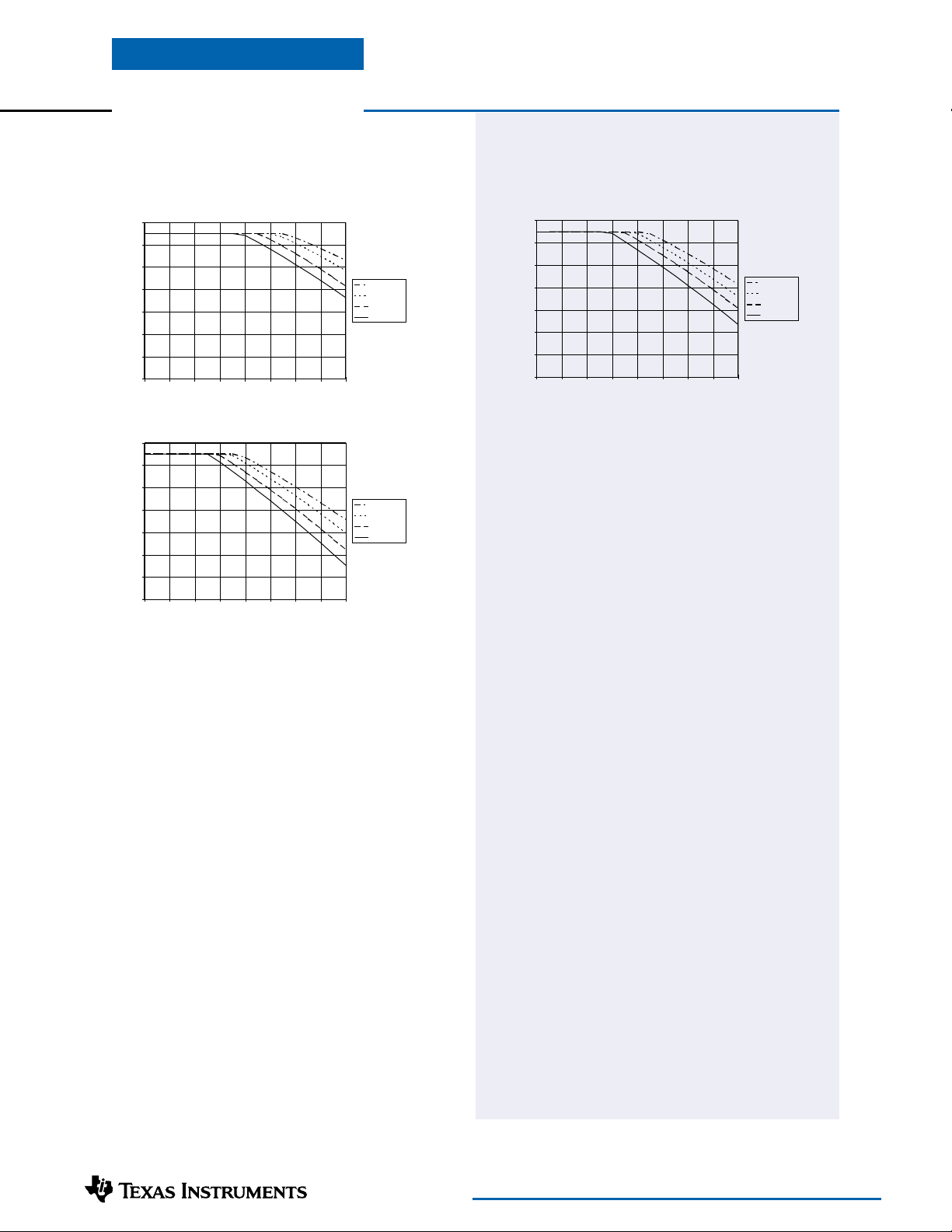
Safe Operating Area; 3.3 V (See Note B) Safe Operating Area; V
=1.2 V
90
80
70
60
50
40
Ambient Temperature (°C)
30
20
012345678
OUT
I
(A
OUT
SLTS220 FEBRUARY 2004
Airflow
200LFM
120LFM
60LFM
Nat Conv
Note B: SOA curves represent the conditions at which internal components are at or below the manufacturer’s maximum operating temperatures
For technical support and further information, visit http://power.ti.com

Application Notes
PT6510 Series
Using the PT6510 Series as a Replacement for the
PT6500 Series in Existing Designs
Scope
The PT6510 series of power modules is the recommended
plug-in replacement for PT6500 series parts. The PT6510
series uses the same single-in-line package (SIP) outlines
and footprint as the PT6500 series, and was designed to be
functionally identical to the PT6500. This application
note highlights the differences in electrical performance
between a PT6510 series replacement compared to an
original PT6500 series part.
Overview
The features that the PT6510 series share with the
PT6500 series includes the output current rating, thermal
shutdown, and on/off standby. The input voltage range,
output voltage adjustment, and output voltage options
are also the same. In addition, applications that use the
PT6510 series as a replacement will experience a number
of performance enhancements. These include improved
efficiency and power dissipation, lower in-rush current
and output ripple voltage. The ‘off’ standby current is
also significantly reduced. Table 1-1 provides a cross
reference between the current PT6500 series part numbers and their equivalent PT6510 series part.
Table 1-1; PT6500 / PT6510 Series Equivalent Parts
PT6500 Series V
OUT
PT6510 Series
PT6501 3.3 V PT6511
PT6502 1.5 V PT6512
PT6503 2.5 V PT6513
PT6504 3.6 V PT6514
PT6505 1.2 V PT6515
PT6506 1.8 V PT6516
Electrical and Functional Differences
Although the PT6510 series was designed as a drop-in
replacement for PT6500 series, there are minor differences
in the electrical characteristics. These are described in the
following text and should be used to assess the replacement part’s compatibility with the system or end product.
A replacement part’s compatibility with the system can
be further verified with appropriate board-level tests.
On/Off Standby: The Standby input of the PT6510 series
is compatible with both the logic polarity and thresholds
of PT6500 series. One exception is the internal pull-up
voltage, which is slightly higher on the PT6510 parts.
The open-circuit voltage for the PT6510 series is the
input voltage, Vin, versus about 1 V for the PT6500 series.
This should not be a problem if the standby input is
controlled with an open-drain transistor with a sufficient
max-Vds rating.
Over-Current & Over-Temperature Protection:
To protect against short circuits and load impedance
faults, the PT6500 employs a constant output current
limit combined with over-temperature shutdown. The
PT6500 will feed a limited steady-state current into a
load fault. When limiting output current, the PT6500
exhibits higher power dissipation, which increases the
module's operating temperature. When its internal temperature rises above the over-temperature threshold, the
module will shut itself down for a few seconds. The
module will then continue to periodically shut down until
the load fault is removed.
The over-current protection mechanism of the PT6510
series is different. If the output current increases above
the modules over-current threshold, its output voltage
is momentarily turned off. It then attempts to recover
by executing a soft-start power up. The module will
continue in a rapid succession of shutdowns and restarts
until the load fault is removed. During this period the
output current is not steady state, but a series of short
high-amplitude pulses (frequency <100 Hz). However,
when operating into a short-circuit load fault, the average
output current and power dissipation are significantly
lower than under normal operation.
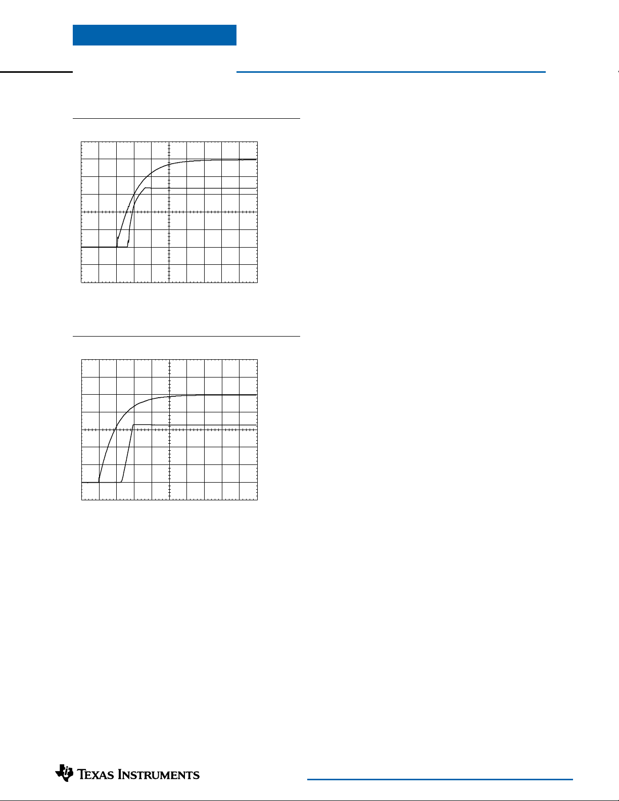
Power-Up Characteristic: Following the application of a
valid input source, the PT6510 series modules exhibit a
slightly longer time delay than the equivalent PT6500
series part. The PT6510 series has a soft-start power-up
feature, which lowers the in-rush current at its input.
Figure 1-1 and Figure 1-2 show the power-up characteristics of the PT6501 and PT6511 respectively. Both
modules have a 3.3-V regulated output, and rise to their
regulated output voltage in a similar period. Note that
the output voltage of the PT6501 begins to rise when
the input voltage reaches 2.2 V, whereas the output voltage
of the PT6511 doesn’t begin to rise until the input voltage
has reached 3.5 V.
For technical support or further information, visit http://power.ti.com
Application Notes
continued
PT6510 Series
Figure 1-1 PT6501 Power-Up Characteristics
HORIZ SCALE: 5 ms/Div
Vin (1 V/Div)
Vout (1 V/Div)
Figure 1-2; PT6511 Power-Up Characterstic
Vin (1 V/Div)
Vo (1 V/Div)
HORIZ SCALE: 5 ms/Div
Conclusion
The differences in electrical performance between the
PT6500 series and the PT6510 series are small. This
should result in only a few, if any, compatibility issues
when a PT6510 series part is used to replace a PT6500
series part in an existing application. In most cases, the
use of a PT6510 part will improve the performance of
the end product over the original PT6500. The performance differences are described to help customers work
through any compatibility issues, and thereby minimize
the impact to their end products. For additional information and questions call Texas Instrument's product
information center (PIC) and request application assistance for plug-in power products.
For technical support and further information, visit http://power.ti.com

Application Notes
PT6510 Series
Capacitor Recommendations for the PT6510 Series of
Integrated Switching Regulators
Input Capacitors:
The recommended input capacitance is determined by
330 µF minimum value (300 µF for Oscon or low-ESR
tantalum types), and 1 A minimum ripple current rating.
Ripple current and less than 100 mΩ equivalent series
resistance (ESR) are the major parameters, along with
temperature, when selecting an input capacitor. Tantalum capacitors have a recommended minimum voltage
rating of twice 2× (max. DC voltage + AC ripple). This
is standard practice to insure reliability.
Output Capacitors:
The ESR of the required output capacitor must not be
greater than 150 mΩ. Electrolytic capacitors have poor
ripple performance at frequencies greater than 400 kHz
but excellent low-frequency transient response. Above
the ripple frequency, ceramic capacitors are necessary to
improve the transient response and reduce any high
frequency noise components apparent during higher
current excursions. Preferred low-ESR type capacitor
part numbers are identified in Table 2-1.
Tantalum Capacitors
Tantalum type capacitors may be used for the output but
only the AVX TPS, Sprague 593D/594/595, or Kemet
T495/T510 series. These capacitors are recommended
over many other tantalum types due to their higher rated
surge, power dissipation, and ripple current capability.
As a caution the TAJ series by AVX is not recommended.
This series has considerably higher ESR, reduced power
dissipation, and lower ripple current capability. The TAJ
series is less reliable than the AVX TPS series when
determining power dissipation capability. Tantalum or
Oscon types are recommended for applications where
ambient temperatures fall below 0 °C.
Capacitor Table
Table 2-1 identifies the characteristics of capacitors from
a number of vendors with acceptable ESR and ripple
current (rms) ratings. The number of capacitors required
at both the input and output buses is identified for each
capacitor type.
This is not an extensive capacitor list. Capacitors from other
vendors are available with comparable specifications. Those listed
are for guidance. The RMS ripple current rating and ESR
(at 100 kHz) are critical parameters necessary to insure both
optimum regulator performance and long capacitor life.
Table 2-1: Suggested Input/Output Capacitors
roticapaC
/rodneV
tnenopmoC
seireS
cinosanaP
CF
detinU
noC-imehC
/SF/VXL
ZXL
nocihciN
MP/LP
cinosanaP
CF
)gtMecafruS(
SS-nocsO
VS
XVA
mulatnaT
SPT
temeK
/015T
594T
eugarpS
D495
gnikroW
egatloV)Fµ(eulaV
V52
V53
V53
V61
V53
V01
V02
V53
V53
V05
V01
V53
V61
V01
V01
V02
V01
V01
V01
V01
V01
V01
V01
RSE.xaM
zHk001ta
Fµ065
Fµ093
Fµ033
Fµ033
Fµ074
Fµ033
Fµ051
065Fµ
033Fµ
074Fµ
0001Fµ
033Fµ
033Fµ
033Fµ
Fµ033
051Fµ
Fµ033
Fµ033
Fµ022
Fµ033
Fµ022
Fµ033
Fµ022
5600.0 Ω
560.0 Ω
711.0 Ω
021.0 Ω
250.0 Ω
520.0 Ω
030.0 ÷2 Ω
840.0 Ω
560.0 ÷2 Ω
640.0 Ω
340.0 Ω
560.0 Ω
051.0 Ω
520.0 Ω
520.0 Ω
420.0 ÷2 Ω
001.0 ÷2 Ω
001.0 ÷2 Ω
590.0 Ω
330.0 Ω
70.0 ÷Ω 530.0=2 Ω
540.0 Ω
560.0 Ω
N/R –Not recommended. The ripple current rating and ESR does not meet the requirements.
scitsiretcarahCroticapaCytitnauQ
)smrI(
Am5021
Am5021
Am555
Am555
Am0221
Am0053
Am0023
Am0631
Am0201
Am0741
Am5021
Am5021
Am076
Am0063
Am0041
Am0532
elppiR.xaM
C°58tatnerruC
Am0053>
Am0083>
Am0052>
Am0003>
Am0002>
Am0002>
Am0002>
eziSlacisyhP
tupnI
)mm(
51x5.21
1
51x5.21
2
5.11x8
21x8
02x01
1
5.01x01
1
5.01x01
2
51x61
1
51x5.21
1
51x81
1
5.61x21
1
61x5.21
1
2.01x01
5.01x0.01
1
3.01x3.01
1
3.01x3.01
2
xL3.7
2
xW3.4
H1.4
H1.4
2
2
W7.5xL3.7
2
H0.4x
2
xL3.7
2
xW0.6
2
tuptuO
suB
suB
1
1
R/N
1
R/N
1
1
1
2
1
1
1
1
1
R/N
1
1
1
2
1
1
2
1
2
1
2
M033SF01
M051SF02
M033SS01
M033VS01
M051VS02
rebmuNrodneV
S165E1CFUEE
S193V1CFUEE
133C1CFUEE
LL21X8M133BV61ZXL
LL02X01M174BV53ZXL
6HHM165V1LPU
6HHM133V1LPU
6HHM1174H1MPU
QL201A1CFVEE
QL133V1CFVEE
P133C1CFVEE
tnuoMecafruS=VS
0010R010M733VSPT
0600R010M733VSPT
0010R5010M722VSPT
SA010M733X015T
SA010M722X594T
T2R0100X733D4
T2D0100X722D495
For technical support or further information, visit http://power.ti.com

Application Notes
PT6510 Series
Using the Standby Function of the PT6510
Series of Integrated Switching Regulators
The PT6510 series of power modules incorporate a
Standby function. This may be used in applications that
require power-up/shutdown sequencing, and wherever
there is a requirement for the output status of the module to be controlled by external circuitry.
The standby function is provided by the STBY* control,
pin 3. If pin 3 is left open-circuit
normally, and provides a regulated output whenever a
valid supply voltage is present at applied to Vin (pins 4-6)
with respect to GND (pins 7–10). Applying a ground
signal to pin 3 disables the regulator’s output and reduces
the input current to about 1 mA 4. The standby control
may also be used to hold off the regulator output during
the period that input power is applied.
Pin 3 is ideally controlled with an open-drain discrete
1
transistor
(See Figure 3-1). It may also be driven directly
from a dedicated TTL 3 compatible gate. Table 3-1 gives
the circuit parameters for the control of this input.
Table 3-1 Standby Control Requirements
Parameter Min Typ Max
Input Low (VIL) –0.1 V 0.4 V
Input High (VIH) 2 V V
Input Low Current (IIL) –0.4 mA
Notes:
1 The standby control input is ideally controlled using an
open-drain discrete transistor. An external pull-up resistor
is not necessary. The open-circuit voltage of the STBY*
pin is the input voltage, V
2. To ensure the regulator output is disabled, the control pin
must be pulled to less than 0.4 Vdc with a low-level
0.5-mA sink to ground.
3. The STBY* input is also compatible with a differential
output from standard TTL logic, providing the IC
shares the same supply voltage as the module.
4. When the regulator output is disabled the current drawn
from the input source is typically reduced to about 1 mA.
1
the regulator operates
(2)
.
in
in
Figure 3-1
1
Vo (Sns)
V
in
COM
Inhibit
4,5,6
Vin Vo
PT6511
Vo Adj
GND
STBY
C
IN
Q1
BSS138
3
V
in
11–13
147–10
C
OUT
V
o
COM
Turn-On Time: In the circuit of Figure 3-1, turning Q1 on
applies a low voltage to the STBY control (pin 3) and
disables the regulator ouput. Correspondingly, turning
off removes the low-voltage signal and enables the
Q
1
output. Once enabled, the output will typically experience
a 10–15 ms delay followed by a predictable ramp-up of
voltage. The regulator should provide a fully regulated
output voltage within 40 ms. The waveform of Figure 3-2
shows the output voltage and input current waveforms of
a PT6511 (3.3 V) following the turn-off of Q
off of Q
corresponds to the rise in Vstby. The waveforms
1
. The turn
1
were measured with a 5 Vdc input voltage, and 4.5 A
resistive load.
Figure 3-2
Vstby (2 V/Div)
HORIZ SCALE: 2 ms/Div
For technical support and further information, visit http://power.ti.com
Vo (1 V/Div)

Application Notes
PT6510 Series
Adjusting the Output Voltage of the
PT6510 5V/3.3V Bus Converters
The output voltage of the PT6510 series switching regulators may be adjusted higher or lower than the factory
trimmed pre-set voltage with the addition of a single
external resistor. Table 4-1 gives the allowable adjustment range for each model in the series as Va (min) and
Va (max).
Adjust Up: An increase in the output voltage is obtained
by adding a resistor R
, between Vo Adjust (pin 14) and
2
GND (pins 7-10).
Adjust Down: Add a resistor (R
(pin 14) and V
(pins 11-13).
out
), between Vo Adjust
1
Refer to Figure 4-1 and Table 4-2 for both the placement and
value of the required resistor, either (R
) or R2 as appropriate.
1
Notes:
1. Use only a single 1 % resistor in either the (R1) or R
location. Place the resistor as close to the ISR as
possible.
2. Never connect capacitors from Vo Adjust to either
GND, V
added to the V
, or the Vo Sense pin. Any capacitance
out
Adjust pin will affect the stability of
o
the ISR.
3. If the remote sense feature is used, connecting the
resistor (R
) between Vo Adjust (pin 14) and Vo Sense
1
(pin 1) can benefit load regulation.
4. The minimum input voltage required by the part is
V
+ 1.2 or Vin(min) from Table 4-1, whichever is
out
higher.
Figure 4-1
1
Vin
4–6
V
in
STBY
+
C
in
COM
The values of (R1) [adjust down], and R2 [adjust up], can
2
also be calculated using the following formulae.
(R1) =
R
2
=
Vo(Sense)
PT6510
GND
3
Ro (Va – 1.0)
– Va)
(V
o
R
- V
V
a
11–13
V
out
(adj)
V
o
147–10
(R1)
Adj Down
R2
Adjust Up
– R
kΩ
s
o
– R
o
kΩ
s
Where: Vo= Original output voltage
Va= Adjusted output voltage
= The resistance value in Table 4-1
R
o
= The series resistance from Table 4-1
R
s
V
out
L
+
COM
O
A
D
C
out
Table 4-1
PT6510 ADJUSTMENT AND FORMULA PARAMETERS
Series Pt # PT6515 PT6512 PT6516 PT6513 PT6511 PT6514
Vo (nom) 1.2 1.5 1.8 2.5 3.3 3.6
Va (min) 1.14 1.27 1.4 1.8 2.25 2.5
Va (max) 2.35 2.65 2.95 3.5 4.2 4.3
ΩΩ
Ro (k
Ω) 2.49 2.49 2.49 4.99 12.1 10
ΩΩ
ΩΩ
Rs (k
Ω) 2 2 2 4.22 12.1 12.1
ΩΩ
Vin(min) 3.1 3.1 3.1 4.5 4.5 4.5
For technical support or further information, visit http://power.ti.com

Application Notes
continued
PT6510 Series
Table 4-2
PT6500 ADJUSTMENT RESISTOR VALUES
Series Pt # PT6515 PT6512 PT6516 PT6513 PT6511 PT6514
Vo (nom) 1.2 V 1.5 V 1.8 V 2.5 V 3.3 V 3.6 V
Va (req’d)
1.15 (5.5) kΩ
1.2
1.25 47.8 kΩ
1.3 22.9 kΩ (1.7) kΩ
1.35 14.6 kΩ (3.8) kΩ
1.4 10.5 kΩ (8.0) kΩ (0.5) kΩ
1.45 8.0 kΩ (20.4) kΩ (1.2) kΩ
1.5 6.3 kΩ (2.2) kΩ
1.55 5.1 kΩ 47.8 kΩ (3.5) kΩ
1.6 4.2 kΩ 22.9 kΩ (5.5) kΩ
1.65 3.5 kΩ 14.6 kΩ (8.8) kΩ
1.7 3.0 kΩ 10.5 kΩ (15.4) kΩ
1.75 2.5 kΩ 8.0 kΩ (35.4) kΩ
1.8 2.2 kΩ 6.3 kΩ (1.5) kΩ
1.85 1.8 kΩ 5.1 kΩ 47.8 kΩ (2.3) kΩ
1.9 1.6 kΩ 4.2 kΩ 22.9 kΩ (3.3) kΩ
1.95 1.3 kΩ 3.5 kΩ 14.6 kΩ (4.4) kΩ
2.0 1.1 kΩ 3.0 kΩ 10.5 kΩ (5.8) kΩ
2.05 0.9 kΩ 2.5 kΩ 8.0 kΩ (7.4) kΩ
2.1 0.8 kΩ 2.2 kΩ 6.3 kΩ (9.5) kΩ
2.15 0.6 kΩ 1.8 kΩ 5.1 kΩ (12.2) kΩ
2.2 0.5 kΩ 1.6 kΩ 4.2 kΩ (15.7) kΩ
2.25 0.4 kΩ 1.3 kΩ 3.5 kΩ (20.7) kΩ (2.3) kΩ
2.3 0.3 kΩ 1.1 kΩ 3.0 kΩ (28.2) kΩ (3.6) kΩ
2.35 0.2 kΩ 0.9 kΩ 2.5 kΩ (40.7) kΩ (5.1) kΩ
2.4 0.8 kΩ 2.2 kΩ (65.6) kΩ (6.7) kΩ
2.45 0.6 kΩ 1.8 kΩ (140.0) kΩ (8.5) kΩ
2.5 0.5 kΩ 1.6 kΩ (10.6) kΩ (1.5) kΩ
2.55 0.4 kΩ 1.3 kΩ 95.6 kΩ (12.9) kΩ (2.7) kΩ
2.6 0.3 kΩ 1.1 kΩ 45.7 kΩ (15.6) kΩ (3.9) kΩ
2.65 0.2 kΩ 6.9 kΩ 29.0 kΩ (18.6) kΩ (5.3) kΩ
2.7 0.8 kΩ 20.7 kΩ (22.2) kΩ (6.8) kΩ
2.75 0.6 kΩ 15.7 kΩ (26.4) kΩ (8.5) kΩ
2.8 0.5 kΩ 12.4 kΩ (31.5) kΩ (10.4) kΩ
2.85 0.4 kΩ 10.0 kΩ (37.6) kΩ (12.6) kΩ
2.9 0.3 kΩ 8.3 kΩ (45.4) kΩ (15.0) kΩ
2.95 0.2 kΩ 0.9 kΩ (55.3) kΩ (17.9) kΩ
3.0 5.8 kΩ (68.6) kΩ (21.2) kΩ
3.1 4.1 kΩ (115.0) kΩ (29.9) kΩ
3.2 2.9 kΩ (254.0) kΩ (42.9) kΩ
3.3 2.0 kΩ (64.6) kΩ
3.4 1.3 kΩ 109.0 kΩ (108.0) kΩ
3.5 0.8 kΩ 48.4 kΩ (238.0) kΩ
3.6 28.2 kΩ
3.7 18.2 kΩ 87.9 kΩ
3.8 12.1 kΩ 37.9 kΩ
3.9
4.0 5.2 kΩ 12.9 kΩ
4.1 3.0 kΩ 7.9 kΩ
4.2 1.3 kΩ 4.6 kΩ
4.3 2.2 kΩ
R1 = (Blue) R2 = Black
4/.
V
>3.8 Vdc requires Vin >5 Vdc ! 8.1 kΩ 21.2 kΩ
out
For technical support and further information, visit http://power.ti.com

MECHANICAL DATA
MPSI013 – MARCH 2001
EEA (R–PSIP–T14) PLASTIC SINGLE-IN-LINE MODULE
1.71 (43,43) MAX.
0.38 0.59
(9,65)
(14,98)
0.018 (0,45)
0.012 (0,30)
0.52
(13,20)
0.175
(4,44)
1.31
(33,27)
1
1
0.100 (2,54) TYP.
0.017 (0,43) TYP.
0.205 (5,20)
1.77 (44,95)
1.42 (36,06)
Note F
ø0.035 (0,88) MIN. 14 Places
Plated through
0.100 (2,54) 13 Places
0.235 (5,96)
1.22 (30,98)
MAX.
Note E
0.20 (5,08)
0.040
0.040 (1,01)
(1,77)0.07
(1,01)
0.42
(10,66)
MAX.
Note G
0.017 (0,43)
TYP.
0.140 (3,55)
MIN.
PC Layout
NOTES: A. All linear dimensions are in inches (mm).
B. This drawing is subject to change without notice.
C. 2-place decimals are
D. 3-place decimals are
E. Recommended mechanical keep-out area.
F. No copper, power or signal traces in this area.
" 0.030 (" 0,76 mm).
" 0.010 (" 0,25 mm).
POST OFFICE BOX 655303 • DALLAS, TEXAS 75265
4202005/A 02/01
G. D-suffix parts include a metal heat spreader.
No signal traces are allowed under the heat spreader area.
A solid copper island is recommended, which may be
grounded.
A-suffix does not include a metal heat spreader.
1

MECHANICAL DATA
MPSI014A – MARCH 2001 – REVISED FEBRUARY 2002
EEK (R–PSIP–G14) PLASTIC SINGLE-IN-LINE MODULE
0.325
(8,25)
0.52
(13,20)
0.205 (5,20)
0.350 (8,89)
0.175
(4,44)
2.36 (62,48) MAX.
2.000 (50,80)
1.71 (43,43) MAX.
0.38
(9,65)
(14,98)
1
1.77
1.42
0.59
0.100 (2,54) TYP.
0.017 (0,43) TYP.
(61,46)
2.42
2.000
(50,80)
(44,95)
(30,06)
ø0.187 (4,74)
2 Places
0.41
(10,41)
1.22 (30,98)
0.83
(21,08)
0.61 (15,49)
0.325
Note E, F
Hole for #6–32 screws
MAX.
0.19 (4,82)
(8,25)
0.080
(2,02)
MIN
0.42
(10,66)
MAX.
Suffix B
Note F
Seating Plane
0.006 (0,15) MAX.
0.10
(2,54)
0.17
(4,32)
0.150
(3,81)
NOTES: A. All linear dimensions are in inches (mm).
B. This drawing is subject to change without notice.
C.
2–place decimals are " 0.030 (" 0,76 mm).
D.
3–place decimals are " 0.010 (" 0,25 mm).
E. Recommended mechanical keep-out area.
F. The metal tab is isolated but electrically conductive.
No signal traces are allowed under the metal tab area.
A solid copper island is recommended, which may be
grounded.
Note H
Note G
0.040 (1,01) 14 Places
0.100 (2,54) 13 Places
0.235 (5,97)
0.350 (8,89)
PC LAYOUT
0.86
(21,84)
1.35
(34,29)
0.64 (16,25)
0.040 (1,01)
0°–7°
Gage Plane
G. Power pin connections should utilize two or more
vias per input, ground and output pin.
H. No copper , power or signal traces in this area.
0.017
TYP.
(0,43)
4202006/B 02/02
POST OFFICE BOX 655303 • DALLAS, TEXAS 75265
1

MECHANICAL DATA
MPSI015A – MARCH 2001 – REVISED JANUARY 2002
EEC (R–PSIP–G14) PLASTIC SINGLE-IN-LINE MODULE
0.52
(13,20)
0.175
(4,44)
1.71 (43,43) MAX.
0.38 0.59
(9,65)
1
(14,98)
0.017 (0,43) TYP.
0.205 (5,20)
1.77 (44,95)
0.100 (2,54) TYP.
1.42 (36,06)
1.22 (30,98)
MAX.
0.080 (2,02) MIN.
Note E, F
0.42
(10,66)
MAX.
Suffix E, C (Note F)
0.018 (0,45)
0.012 (0,30)
Note F
Seating Plane
0.006 (0,15) MAX.
Note H
1
0.150
(3,81)
0.235 (5,96)
NOTES: A. All linear dimensions are in inches (mm).
B. This drawing is subject to change without notice.
C.
2–place decimals are " 0.030 (" 0,76 mm).
D.
3–place decimals are " 0.010 (" 0,25 mm).
E. Recommended mechanical keep-out area.
F. E-suffix parts include a metal heat spreader.
No signal traces are allowed under the heat spreader area.
A solid copper island is recommended, which may be
grounded.
C-suffix does not include a metal heat spreader.
See Note G
0.040 (1,01) 14 Places
0.100 (2,54) 13 Places
PC LAYOUT
1.35
(34,29)
0°–7°
Gage Plane
0.10 (2,54)
0.17 (4,31)
G. Power pin connections should utilize two or more
vias per input, ground and output pin.
H. No copper , power or signal traces in this area.
0.040 (1,01)
TYP
(0,43)0.017
4202007/B 12/01
POST OFFICE BOX 655303 • DALLAS, TEXAS 75265
1

MECHANICAL DATA
MPSI016A – MARCH 2001 – REVISED FEBRUARY 2002
EEG (R–PSIP–T14) PLASTIC SINGLE-IN-LINE MODULE
0.325
(8,25)
0.52
(13,20)
0.205 (5,20)
0.350 (8,89)
0.175
(4,44)
2.36 (62,48) MAX.
2.000 (50,80)
1.71 (43,43) MAX.
0.59
(14,98)
1
2.42
2.000
1.77
1.42
0.38 (9,65)
0.100 (2,54) TYP.
0.017 (0,43) TYP.
(61,46)
(50,80)
(44,95)
(30,06)
ø0.187 (4,74)
2 Places
0.41 (10,41)
1.22 (30,98)
0.83
(21,08)
0.61
(15,49)
(8,25)
0.325
Note E, F
Hole for #6–32 screws
MAX.
0.19
(4,82)
0.040
(1,01)
0.42
(10,66)
MAX.
Suffix G
Note F
0.017
(0,43)
TYP.
0.140
(3,55)
MIN.
0.20
(5,08)
0.07
(1,77)
NOTES: A. All linear dimensions are in inches (mm).
B. This drawing is subject to change without notice.
C. 2-place decimals are
D. 3-place decimals are
E. Recommended mechanical keep-out area.
F. The metal tab is isolated but electrically conductive.
No signal traces are allowed under the metal tab area.
A solid copper island is recommended, which may be grounded.
G. No copper , power or signal traces in this area.
Note G
ø0.035 (0,88) MIN. 14 Places
Plated through
0.100 (2,54) 13 Places
0.235 (5,97)
0.350 (8,89)
PC LAYOUT
" 0.030 (" 0,76 mm).
" 0.010 (" 0,25 mm).
0.65
(16,51)
0.86
(21,84)
0.040 (1,01)
1.31
(33,27)
4202008/B 02/02
POST OFFICE BOX 655303 • DALLAS, TEXAS 75265
1

MECHANICAL DATA
MPSI017 – MARCH 2001
EED (R–PSIP–T14) PLASTIC SINGLE-IN-LINE MODULE
1.71 (43,43) MAX.
0.38 0.59
(9,65)
(14,98)
0.018 (0,45)
0.012 (0,30)
0.52
(13,20)
1
1
0.100 (2,54) TYP.
0.017 (0,43) TYP.
0.205 (5,20)
1.77 (44,95)
0.235 (5,96)
0.100 (2,54) 13 Places
ø0.035 (0,88) MIN. 14 Places
Plated through
1.22 (30,98)
MAX.
0.170 (4,31) MIN.
0.040 (1,01)
0.42
(10,66)
Note E
Note F
0.017 (0,43) TYP.
0.42
(10,66)
MAX.
PC LAYOUT
NOTES: A. All linear dimensions are in inches (mm).
B. This drawing is subject to change without notice.
C. 2-place decimals are
D. 3-place decimals are
E. Recommended mechanical keep-out area.
F. P-suffix parts include a metal heat spreader.
The heat spreader is isolated but electrically
conductive, it can be grounded.
N-suffix does not include a metal heat spreader.
" 0.030 (" 0,76 mm).
" 0.010 (" 0,25 mm).
POST OFFICE BOX 655303 • DALLAS, TEXAS 75265
4202009/A 02/01
1

MECHANICAL DATA
MPSI018A – MARCH 2001 – REVUSED FEBRUARY 2002
EEE (R–PSIP–T14) PLASTIC SINGLE-IN-LINE MODULE
Suffix R
2.36 (62,48) MAX.
2.000 (50,80)
1.71 (43,43) MAX.
ø0.187 (4,74)
2 Places
0.41 (10,41)
0.325
(8,25)
0.38 (9,65)
0.59
(14,98)
0.52
(13,20)
0.205 (5,20)
0.350 (8,89)
0.07
(1,77)
0.11
(2,79)
0.325
(8,25)
1
1
Note E
0.100 (2,54) TYP.
0.017 (0,43) TYP.
2.42 (61,46)
1.77 (44,95)
0.100 (2,54) 13 Places
0.235 (5,96)
ø0.035 (0,88) MIN. 14 Places
Plated through
PC LAYOUT
0.61
(15,49)
0.040 (1,01)
0.42
(10,66)
0.83
(21,08)
1.22 (30,98)
MAX.
0.19
(4,82)
0.170
(4,31)
MIN.
0.42
(10,66)
MAX.
Note F
0.017
(0,43)
TYP.
4202010/B 02/02
NOTES: A. All linear dimensions are in inches (mm).
B. This drawing is subject to change without notice.
C. 2-place decimals are
D. 3-place decimals are
E. Recommended mechanical keep-out area.
F. The metal tab is isolated but electrically
conductive, it can be grounded.
" 0.030 (" 0,76 mm).
" 0.010 (" 0,25 mm).
POST OFFICE BOX 655303 • DALLAS, TEXAS 75265
1

MECHANICAL DATA
MPSI019A – MARCH 2001 – REVISED FEBRUARY 2002
EEF (R–PSIP–G14) PLASTIC SINGLE-IN-LINE MODULE
0.325
(8,25)
0.87
(22,11)
0.52
(13,20)
0.205 (5,20)
0.350 (8,89)
0.175
(4,44)
2.36 (62,48) MAX.
2.000 (50,80)
1.71 (43,43) MAX.
0.38
(9,65)
1
0.59
(14,98)
2.42
2.000
1.77
1.42
0.71
(18,07)
0.100 (2,54) TYP.
0.017 (0,43) TYP.
(61,46)
(50,80)
(44,95)
(30,06)
ø0.187 (4,74)
2 Places
0.41 (10,41)
1.22 (30,98)
0.83
(21,08)
0.61
(15,49)
0.325 (8,25)
0.19 (4,82)
Note E,F
Hole for #6–32 screws
MAX.
0.040 (1,01)
0.19 (4,82)
0.210 (5,33)
0.080
(2,02)
MIN.
Gage Plane
0°–7°
0.42
(10,66)
MAX.
Suffix F
Note J
Note F
Seating Plane
0.006 (0,15) MAX.
0.040 (1,01)
0.017 (0,43) TYP.
0.10
(2,54)
0.17
(4,32)
0.150
(3,81)
NOTES: A. All linear dimensions are in inches (mm).
B. This drawing is subject to change without notice.
C. 2-place decimals are
D. 3–place decimal are
E. Recommended mechanical keep-out area.
F. The metal tab is isolated but electrically conductive.
No signal traces are allowed under the metal tab area.
A solid copper island is recommended, which may be
grounded.
G. Power pin connections should utilize two or more
vias per input, ground and output pin.
0.545
(13,84)
CtoC
L
L
Note L
Note G
0.040 (1,01) 14 Places
0.100 (2,54) 13 Places
0.235 (5,97)
0.350 (8,89)
PC LAYOUT
" 0.030 (" 0,76 mm).
" 0.010 (" 0,25 mm).
(21,84)
0.64
(16,25)
0.86
1.35
(34,29)
1.120
(28,44)
to
C
C
LL
H. Minimum copper land area required for solder tab.
Vias are recommended to improve copper adhesion
or connect land to other ground area.I
J. Underside solder tabs detail.
K. Solder mask openings to copper island for solder
joints to mechanical pins.
L. No copper, power or signal traces in this area.
0.33
(8,38)
0.280
(7,11)
0.085
(2,16)
0.080 (2,03) 2 Places
Note H
0.210
(5,33)
0.38
(9,65)
4202011/B 02/02
Note K
POST OFFICE BOX 655303 • DALLAS, TEXAS 75265
1

MECHANICAL DATA
MPSI020 – MARCH 2001
EEL (R–PSIP–G14) PLASTIC SINGLE-IN-LINE MODULE
0.87
(22,11)
0.52
(13,20)
0.205 (5,20)
0.175 (4,44)
1.71 (43,43) MAX.
0.38
(9,65)
(14,98)
1
1.42
0.59
1.77
(18,07)
0.100 (2,54) TYP.
0.017 (0,43) TYP.
(44,95)
(30,06)
0.71
1.22 (30,98)
MAX.
0.19 (4,82)
0.210 (5,33)
Note E
0.040 (1,01)
0.080 (2,02) MIN.
0°–7°
Gage Plane
Note J
0.42
(10,66)
MAX.
0.042
(1,06)
0.036(0,91)
Note F
Seating Plane
0.006 (0,15) MAX.
0.040
(1,01)
0.017
(0,43)
TYP.
0.10
(2,54)
0.17 (4,32)
0.150 (3,81)
NOTES: A. All linear dimensions are in inches (mm).
B. This drawing is subject to change without notice.
C.
2–place decimals are " 0.030 (" 0,76 mm).
D.
3–place decimals are " 0.010 (" 0,25 mm).
E. Recommended mechanical keep-out area.
F. The metal tab is isolated but electrically conductive.
No signal traces are allowed under the metal tab area.
A solid copper island is recommended, which may be
grounded.
G. Power pin connections should utilize two or more
vias per input, ground and output pin.
0.545
(13,84)
CtoC
L
L
Note L
Note G
0.035 (0,88) 14 Places
0.100 (2,54) 13 Places
0.235 (5,97)
PC LAYOUT
1.120
(28,44)
to
C
C
LL
1.35
(34,29)
0.080
0.280
0.33
(7,11)
(8,38)
0.085 (2,16)
H. Minimum copper land area required for solder tab.
Vias are recommended to improve copper adhesion
or connect land to other ground area.
J. Underside solder tabs detail
K. Solder mask openings to copper island for solder
joints to mechanical pins.
L. No copper, power or signal traces in this area.
0.210
(5,33)
0.38
(9,65)
2 Places
(2,03)
Note H
Note K
4202012/A 02/01
POST OFFICE BOX 655303 • DALLAS, TEXAS 75265
1

IMPORTANT NOTICE
Texas Instruments Incorporated and its subsidiaries (TI) reserve the right to make corrections, modifications,
enhancements, improvements, and other changes to its products and services at any time and to discontinue
any product or service without notice. Customers should obtain the latest relevant information before placing
orders and should verify that such information is current and complete. All products are sold subject to TI’s terms
and conditions of sale supplied at the time of order acknowledgment.
TI warrants performance of its hardware products to the specifications applicable at the time of sale in
accordance with TI’s standard warranty. Testing and other quality control techniques are used to the extent TI
deems necessary to support this warranty . Except where mandated by government requirements, testing of all
parameters of each product is not necessarily performed.
TI assumes no liability for applications assistance or customer product design. Customers are responsible for
their products and applications using TI components. To minimize the risks associated with customer products
and applications, customers should provide adequate design and operating safeguards.
TI does not warrant or represent that any license, either express or implied, is granted under any TI patent right,
copyright, mask work right, or other TI intellectual property right relating to any combination, machine, or process
in which TI products or services are used. Information published by TI regarding third-party products or services
does not constitute a license from TI to use such products or services or a warranty or endorsement thereof.
Use of such information may require a license from a third party under the patents or other intellectual property
of the third party, or a license from TI under the patents or other intellectual property of TI.
Reproduction of information in TI data books or data sheets is permissible only if reproduction is without
alteration and is accompanied by all associated warranties, conditions, limitations, and notices. Reproduction
of this information with alteration is an unfair and deceptive business practice. TI is not responsible or liable for
such altered documentation.
Resale of TI products or services with statements different from or beyond the parameters stated by TI for that
product or service voids all express and any implied warranties for the associated TI product or service and
is an unfair and deceptive business practice. TI is not responsible or liable for any such statements.
Following are URLs where you can obtain information on other Texas Instruments products and application
solutions:
Products Applications
Amplifiers amplifier.ti.com Audio www.ti.com/audio
Data Converters dataconverter.ti.com Automotive www.ti.com/automotive
DSP dsp.ti.com Broadband www.ti.com/broadband
Interface interface.ti.com Digital Control www.ti.com/digitalcontrol
Logic logic.ti.com Military www.ti.com/military
Power Mgmt power.ti.com Optical Networking www.ti.com/opticalnetwork
Microcontrollers microcontroller.ti.com Security www.ti.com/security
Telephony www.ti.com/telephony
Video & Imaging www.ti.com/video
Wireless www.ti.com/wireless
Mailing Address: Texas Instruments
Post Office Box 655303 Dallas, Texas 75265
Copyright 2004, Texas Instruments Incorporated

Copyright © Each Manufacturing Company.
All Datasheets cannot be modified without permission.
This datasheet has been download from :
www.AllDataSheet.com
100% Free DataSheet Search Site.
Free Download.
No Register.
Fast Search System.
www.AllDataSheet.com
 Loading...