

Auto-Track™
Sequencing
查询PTH12050L供应商
PTH12050W/L —12-V Input
6-A, 12-V Input Non-Isolated
Wide-Output Adjust Power Module
NOMINAL SIZE = 0.87 in x 0.5 in
(22,1 mm x 12,57 mm)
Description
The PTH12050 series is the smallest
non-isolated power modules from Texas
Instruments that features Auto-Track™
Sequencing. Auto-Track simplifies the
sequencing of supply voltages in power
systems by enabling modules to track each
other, or any other external voltage, during
power up and power down.
Although small in size (0.87 in × 0.5 in),
these modules are rated for up to 6 A of
output current, and are an ideal choice in
applications where space, performance,
and a power-up sequencing capability are
important attributes.
The series operates from an input
voltage of 12-V to provide step-down
conversion to a wide range of output volt-
Features
• Up to 6-A Output Current
• 12-V Input Voltage
• Wide-Output Voltage Adjust
(1.2 V to 5.5 V)/(0.8 V to 1.8 V)
• Efficiencies up to 93 %
• 200 W/in³ Power Density
• On/Off Inhibit
• Under-Voltage Lockout
• Operating Temp: –40 to +85 °C
ages. The output voltage of the W-suffix
device may set to any voltage over the
adjust range, 1.2 V to 5.5 V. The L-suffix
device has an adjustment range of 0.8 V
to 1.8 V. The output voltage is set within
the adjustment range using a single external resistor.
Other operating features include an
on/off inhibit, output voltage adjust (trim),
and output over-current protection. For
high efficiency these parts employ a synchronous rectifier output stage.
Target applications include telecom,
industrial, and general purpose circuits,
including low-power dual-voltage systems
that use a DSP, microprocessor, ASIC, or
FPGA.
• Auto-Track™ Sequencing
• Output Over-Current Protection
• IPC Lead Free 2
• Safety Agency Approvals:
• Point-of-Load Alliance (POLA)
SLTS214C – MAY 2003 – REVISED MARCH 2003
(Non-Latching, Auto-Reset)
UL 60950, cUL 600950, EN60950
(VDE is Pending)
Compatible
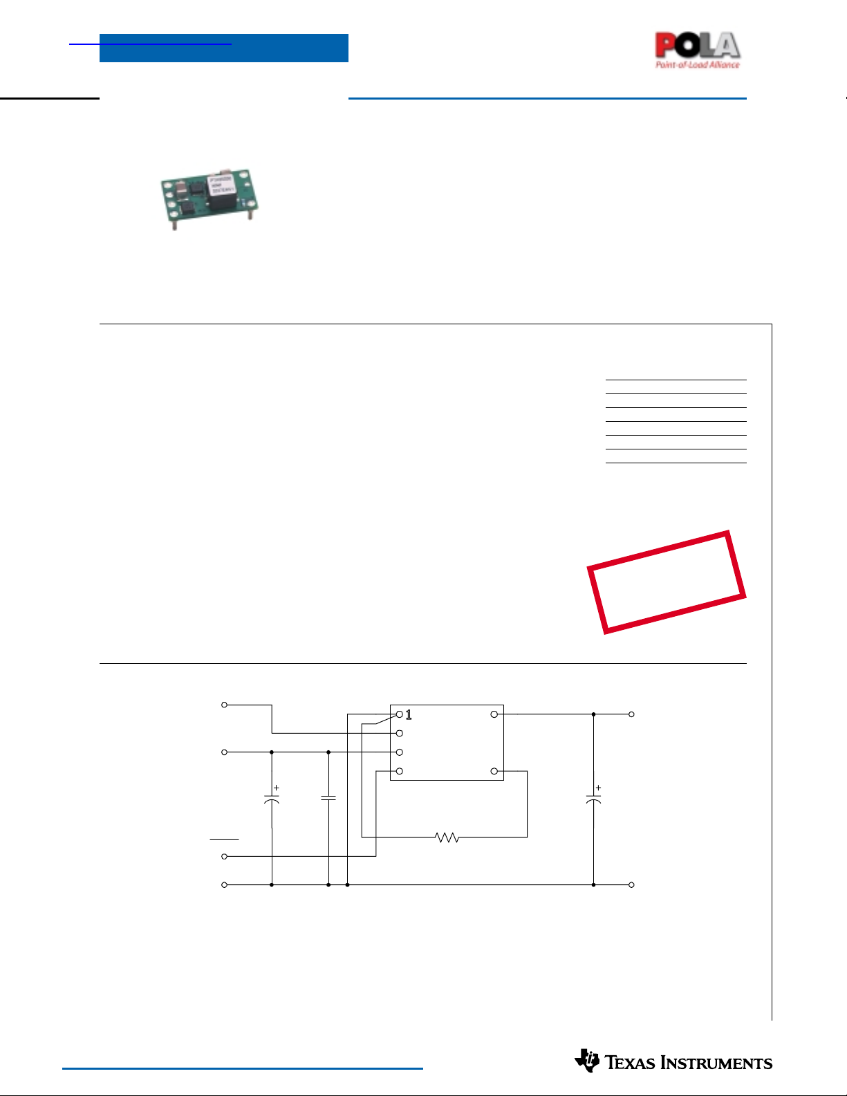
Pin Configuration
Pin Function
1 GND
2 Track
3V
in
4 Inhibit *
5Vo Adjust
6V
out
* Denotes negative logic:
Open = Normal operation
Ground = Function active
Standard Application
Track
V
IN
C
1
100 µF
(Required)
Inhibit
GND
For technical support and further information, visit http://power.ti.com
C
2
10 µF
Ceramic
1
2
3
4
PTH12050
(Top View)
R
SET
1 %,
(Required)
V
6
5
C
3
100 µF
(Optional)
R
= Required to set the output voltage higher than
set
the lowest value. (See spec. table for values)
C
= Required 100 µF capacitor
1
C
= 10 µF ceramic capacitor. Required for output
2
voltages 3.3 V and higher
C
= Optional 100 µF capacitor
3
OUT
GND
PTH12050W/L —12-V Input
6-A, 12-V Input Non-Isolated
Wide-Output Adjust Power Module
Ordering Information
Output Voltage
Code Voltage
W 1.2 V – 5.5 V (Adjust)
L 0.8 V – 1.8 V (adjust)
Notes: (1) Add “T” to end of part number for tape and reel on SMD packages only.
(2) Reference the applicable package reference drawing for the dimensions and PC board layout
(3) “Standard” option specifies 63/37, Sn/Pb pin solder material.
(PTH12050Hxx)
Package Options
Code Description Pkg Ref.
AH Horiz. T/H (EUU)
AS SMD, Standard
(PTH12050xHH)
Pin Descriptions
Vin: The positive input voltage power node to the mod-
ule, which is referenced to common GND.
Vout: The regulated positive power output with respect
to the GND node.
GND: This is the common ground connection for the
Vin and Vout power connections. It is also the 0 VDC
reference for the control inputs.
Vo Adjust: A 1 % resistor must be directly connected between this pin and GND (pin 1) to set the output voltage
of the module to a value higher than its lowest value.
The temperature stability of the resistor should be
100 ppm/°C (or better). The set-point range is 1.2 V to
5.5 V for W-suffix devices, and 0.8 V to 1.8 V for L-suffix
devices. The resistor value required for a given output
voltage may be calculated using a formula. If left open
circuit, the output voltage will default to its lowest value.
For further information on output voltage adjustment
consult the related application note.
The specification table gives the preferred resistor values
for a number of standard output voltages.
SLTS214C – MAY 2003 – REVISED MARCH 2003
(1)
(2)
(3)
(EUV)
Inhibit: The Inhibit pin is an open-collector/drain negative logic input that is referenced to GND. Applying a
low-level ground signal to this input disables the module’s
output and turns off the output voltage. When the Inhibit
control is active, the input current drawn by the regulator
is significantly reduced. If the Inhibit pin is left opencircuit, the module will produce an output whenever a
valid input source is applied.
Track: This is an analog control input that enables the
output voltage to follow an external voltage. This pin
becomes active typically 20 ms after the input voltage
has been applied, and allows direct control of the output
voltage from 0 V up to the nominal set-point voltage.
Within this range the output will follow the voltage at
the Track pin on a volt-for-volt basis. When the control
voltage is raised above this range, the module regulates
at its set-point voltage. The feature allows the output
voltage to rise simultaneously with other modules powered from the same input bus. If unused, the input should
be connected to V
. Note: Due to the under-voltage lockout
in
feature, the output of the module cannot follow its own input
voltage during power up. For more information, consult the
related application note.
Environmental & Absolute Maximum Ratings (Voltages are with respect to GND)
Characteristics Symbols Conditions Min Typ Max Units
Track Input Voltage V
Operating Temperature Range T
Solder Reflow Temperature T
Storage Temperature T
Mechanical Shock Per Mil-STD-883D, Method 2002.3
Mechanical Vibration Mil-STD-883D, Method 2007.2
Weight — — 2.9 — grams
Flammability — Meets UL 94V-O
Notes: (i) During reflow of SMD package version do not elevate peak temperature of the module, pins or internal components above the stated maximum.
track
a
reflow
s
Over Vin Range –40 — 85 °C
Surface temperature of module body or pins 235
— –40 — 125 °C
1 msec, ½ Sine, mounted
20-2000 Hz
–0.3 — Vin + 0.3 V
(i)
— 500 — G’s
—20— G’s
For technical support and further information, visit http://power.ti.com
°C
PTH12050W —12-V Input
6-A, 12-V Input Non-Isolated
Wide-Output Adjust Power Module
Specifications (Unless otherwise stated, T
=25 °C, Vin =12 V, V
a
=3.3 V, C1=100 µF, C2 =10 µF, C3 =0 µF, and Io =Iomax)
out
SLTS214C – MAY 2003 – REVISED MARCH 2003
PTH12050W
Characteristics Symbols Conditions Min Typ Max Units
Over ∆V
Output Current I
Input Voltage Range V
o
in
range 85 °C, 400 LFM airflow 0 — 6
adj
60 °C, natural convection 0 — 6
Over Io range 10.8 — 13.2 V
Set-Point Voltage Tolerance Vo tol — — ±2
Temperature Variation ∆Reg
Line Regulation ∆Reg
Load Regulation ∆Reg
Total Output Variation ∆Reg
Ouput Voltage Adjust Range ∆V
temp
line
load
tot
adj
Efficiency η I
Vo Ripple (pk-pk) V
r
–40 °C <Ta < +85 °C — ±0.5 — %V
Over Vin range — ±5 — mV
Over Io range — ±5 — mV
Includes set-point, line, load,
–40 °C ≤ Ta ≤ +85 °C
——±3
Over Vin range 1.2 — 5.5 V
=5 A R
o
20 MHz bandwidth V
= 280 Ω Vo = 5.0 V — 93 —
SET
= 2.0 kΩ Vo = 3.3 V — 91 —
R
SET
= 4.32 kΩ Vo = 2.5 V — 89 —
R
SET
= 8.06 kΩ Vo = 2.0 V — 88 — %
R
SET
= 11.5 kΩ Vo = 1.8 V — 87 —
R
SET
R
= 24.3 kΩ Vo = 1.5 V — 86 —
SET
R
= open cct V
SET
= 1.2 V — 84 —
o
≤2.5 V — 25 — mVpp
o
V
>2.5 V — 1 — % V
o
(1)
(1)
(2)
(2)
Over-Current Threshold Io trip Reset, followed by auto-recovery — 14 — A
Transient Response 1 A/µs load step, 50 to 100 % I
t
tr
∆V
tr
=100 µF
C
3
Track Input Current (pin 2) IIL track Pin to GND — — –0.13
Track Slew Rate Capability dV
Under-Voltage Lockout UVLO V
Inhibit Control (pin 4) Referenced to GND
Input High Voltage V
Input Low Voltage
Input Low Current
V
I
IL
track
IH
IL
inhibit
/dt C
≤C
(max) — — 1 V/ms
out
out
increasing — 9.5 10.4
in
Vin decreasing 8.8 9 —
Pin to GND — –0.24 — mA
max,
o
Recovery Time — 70 — µSec
Vo over/undershoot — 100 — mV
Vin –0.5 — Open
–0.2 — 0.5
(3)
(3)
Input Standby Current Iin inh Inhibit (pin 4) to GND, Track (pin 2) open — 10 — mA
Switching Frequency ƒ
External Input Capacitance C
External Output Capacitance C
s
1
3
Reliability MTBF Per Bellcore TR-332
Notes:
(1) See SOA curves or consult factory for appropriate derating.
(2) The set-point voltage tolerance is affected by the tolerance and stability ofR
with 100 ppm/°C or better temperature stability.
(3) This control pin has an internal pull-up to the input voltage Vin (7.5 V for pin 2). If it is left open-circuit the module will operate when input power is
applied. A small low-leakage (<100 nA) MOSFET is recommended for control. For further information, consult the related application note.
(4) A 100 µF electrolytic input capacitor is required for proper operation. The electrolytic capacitor must be rated for a minimum of 750 mA rms of ripple
current. An additional 10 µF ceramic capacitor is required for output voltages 3.3 V and higher. For further information, consult the related application
note on capacitor selection.
(5) An external output capacitor is not required for basic operation. Adding 100 µF of distributed capacitance at the load will improve the transient response.
(6) This is the calculated maximum. The minimum ESR limitation will often result in a lower value. Consult the application notes for further guidance.
(7) This is the typcial ESR for all the electrolytic (non-ceramic) output capacitance. Use 7 m
Over Vin and Io ranges 260 320 380 kHz
(4)
100
Capacitance value non-ceramic 0 100
Equiv. series resistance (non-ceramic) 4
50 % stress, Ta =40 °C, ground benign
SET
ceramic 0 — 300
(7)
5.9 — — 10
. The stated limit is unconditionally met if R
Ω
as the minimum when using max-ESR values to calculate.
——µF
(5)
3,300
(6)
——
has a tolerance of 1 %
SET
A
%V
%V
mA
V
V
µF
6
o
o
o
o
Hrs
For technical support and further information, visit http://power.ti.com
PTH12050W —12-V Input
)
Typical Characteristics
6-A, 12-V Input Non-Isolated
Wide-Output Adjust Power Module
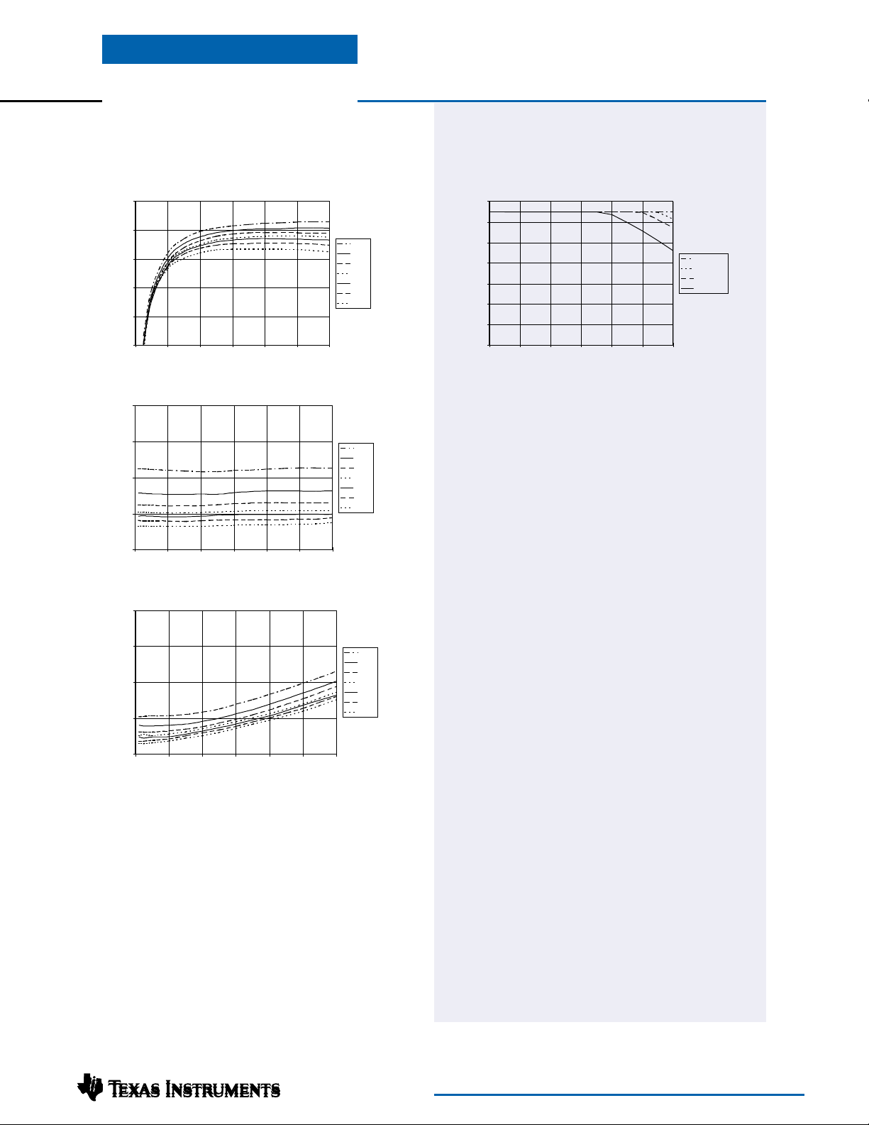
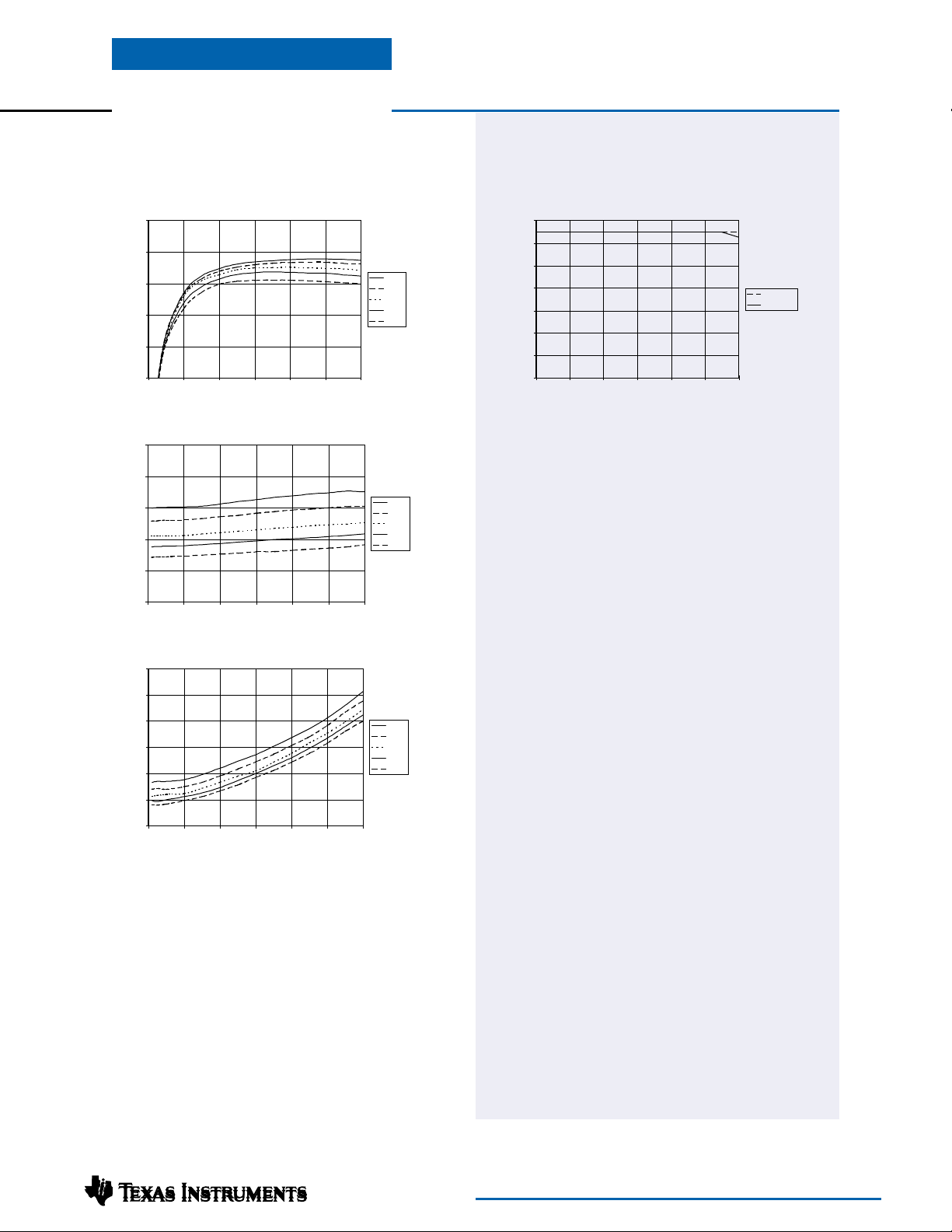
PTH12050W Characteristic Data; Vin =12 V (See Note A)
Efficiency vs Load Current
100
V
V
OUT
5.0 V
3.3 V
2.5 V
2.0 V
1.8 V
1.5 V
1.2 V
OUT
5.0 V
3.3 V
2.5 V
2.0 V
1.8 V
1.5 V
1.2 V
90
80
70
Efficiency - %
60
50
0123456
Output Ripple vs Load Current
80
60
40
Ripple - mV
20
Iout - Amps
SLTS214C – MAY 2003 – REVISED MARCH 2003
PTH12050W Safe Operating Area; Vin =12 V (See Note B)
All Output Voltages
90
80
70
60
50
40
Ambient Temperature (°C)
30
20
0123456
Iout (A
Airflow
400LFM
200LFM
100LFM
Nat Conv
0
0123456
Power Dissipation vs Load Current
4
3
2
Pd - Watts
1
0
0123456
Iout - Amps
Iout - Amps
V
OUT
5.0 V
3.3 V
2.5 V
2.0 V
1.8 V
1.5 V
1.2 V
Note A: Characteristic data has been developed from actual products tested at 25°C. This data is considered typical data for the Converter.
Note B: SOA curves represent the conditions at which internal components are at or below the manufacturer’s maximum operating temperatures. Derating limits apply to
modules soldered directly to a 4 in.
×
4 in. double-sided PCB with 1 oz. copper.
For technical support and further information, visit http://power.ti.com
PTH12050L —12-V Input
6-A, 12-V Input Non-Isolated
Wide-Output Adjust Power Module
Specifications (Unless otherwise stated, T
=25 °C, Vin =12 V, V
a
=1.8 V, C1=100 µF, C2 =10 µF, C3 =0 µF, and Io =Iomax)
out
SLTS214C – MAY 2003 – REVISED MARCH 2003
PTH12050L
Characteristics Symbols Conditions Min Typ Max Units
Over ∆V
Output Current I
Input Voltage Range V
o
in
range 85 °C, 400 LFM airflow 0 — 6
adj
60 °C, natural convection 0 — 6
Over Io range 10.8 — 13.2 V
Set-Point Voltage Tolerance Vo tol — — ±2
Temperature Variation ∆Reg
Line Regulation ∆Reg
Load Regulation ∆Reg
Total Output Variation ∆Reg
Ouput Voltage Adjust Range ∆V
temp
line
load
tot
adj
Efficiency η I
Vo Ripple (pk-pk) V
r
–40 °C <Ta < +85 °C — ±0.5 — %V
Over Vin range — ±5 — mV
Over Io range — ±5 — mV
Includes set-point, line, load,
–40 °C ≤ Ta ≤ +85 °C
——±3
Over Vin range 0.8 — 1.8 V
=5 A R
o
20 MHz bandwidth Vo >1.0 V — 30 —
= 130 Ω Vo = 1.8 V — 88 —
SET
= 3.57 kΩ Vo = 1.5 V — 87 —
R
SET
= 12.1 kΩ Vo = 1.2 V — 85 — %
R
SET
= 32.4 kΩ Vo = 1.0 V — 83 —
R
SET
R
= open cct V
SET
= 0.8 V — 81 —
o
V
≤1.0 V — 20 —
o
(1)
(1)
(2)
(2)
Over-Current Threshold Io trip Reset, followed by auto-recovery — 14 — A
Transient Response 1 A/µs load step, 50 to 100 % Iomax,
t
tr
∆V
tr
Track Input Current (pin 2) IIL track Pin to GND — — –0.13
Track Slew Rate Capability dV
/dt C
track
Under-Voltage Lockout UVLO Vin increasing — 9.5 10.4
Inhibit Control (pin 4) Referenced to GND
Input High Voltage V
Input Low Voltage
Input Low Current
V
I
IL
IH
IL
inhibit
=100 µF
C
3
≤C
(max) — — 1 V/ms
out
out
Recovery Time — 70 — µSec
Vo over/undershoot — 100 — mV
(3)
Vin decreasing 8.8 9 —
Vin –0.5 — Open
–0.2 — 0.5
(3)
Pin to GND — –0.24 — mA
Input Standby Current Iin inh Inhibit (pin 4) to GND, Track (pin 2) open — 10 — mA
Switching Frequency ƒ
External Input Capacitance C
External Output Capacitance C
s
1
3
Reliability MTBF Per Bellcore TR-332
Notes:
(1) See SOA curves or consult factory for appropriate derating.
(2) The set-point voltage tolerance is affected by the tolerance and stability ofR
with 100 ppm/°C or better temperature stability.
(3) This control pin has an internal pull-up to the input voltage Vin (7.5 V for pin 2). If it is left open-circuit the module will operate when input power is
applied. A small low-leakage (<100 nA) MOSFET is recommended for control. For further information, consult the related application note.
(4) A 100 µF electrolytic input capacitor is required for proper operation. The electrolytic capacitor must be rated for a minimum of 750 mA rms of ripple
current. An additional 10 µF ceramic capacitor is required for output voltages 3.3 V and higher. For further information, consult the related application
note on capacitor selection.
(5) An external output capacitor is not required for basic operation. Adding 100 µF of distributed capacitance at the load will improve the transient response.
(6) This is the calculated maximum. The minimum ESR limitation will often result in a lower value. Consult the application notes for further guidance.
(7) This is the typcial ESR for all the electrolytic (non-ceramic) output capacitance. Use 7 m
Over Vin and Io ranges 200 250 300 kHz
(4)
100
Capacitance value non-ceramic 0 100
Equiv. series resistance (non-ceramic) 4
50 % stress, Ta =40 °C, ground benign
SET
ceramic 0 — 300
(7)
5.9 — — 10
. The stated limit is unconditionally met if R
Ω
as the minimum when using max-ESR values to calculate.
——µF
(5)
3,300
(6)
——
has a tolerance of 1 %
SET
A
%V
%V
mVpp
mA
V
V
µF
6
Hrs
o
o
o
For technical support and further information, visit http://power.ti.com
PTH12050L —12-V Input
)
Typical Characteristics
6-A, 12-V Input Non-Isolated
Wide-Output Adjust Power Module
PTH12050L Characteristic Data; Vin =12 V (See Note A)
Efficiency vs Load Current
100
90
80
70
Efficiency - %
60
50
0123456
Output Ripple vs Load Current
50
40
30
20
Ripple - mV
10
Iout - Amps
V
OUT
1.8 V
1.5 V
1.2 V
1.0 V
0.8 V
V
OUT
1.8 V
1.5 V
1.2 V
1.0 V
0.8 V
SLTS214C – MAY 2003 – REVISED MARCH 2003
PTH12050L Safe Operating Area; Vin =12 V (See Note B)
PTH12050L; V
90
80
70
60
50
40
Ambient Temperature (°C)
30
20
0123456
OUT
≤≤
≤1.8 V
≤≤
Iout (A
Airflow
100LFM
Nat conv
0
0123456
Power Dissipation vs Load Current
1.8
1.5
1.2
0.9
Pd - Watts
0.6
0.3
0
0123456
Iout - Amps
Iout - Amps
V
OUT
1.8 V
1.5 V
1.2 V
1.0 V
0.8 V
Note A: Characteristic data has been developed from actual products tested at 25°C. This data is considered typical data for the Converter.
Note B: SOA curves represent the conditions at which internal components are at or below the manufacturer’s maximum operating temperatures. Derating limits apply to
modules soldered directly to a 4 in.
×
4 in. double-sided PCB with 1 oz. copper.
For technical support and further information, visit http://power.ti.com

Application Notes
PTH12050 Series
Capacitor Recommendations for the PTH12050
Series of Power Modules
Input Capacitor
The recommended input capacitor(s) is determined by
the 100 µF minimum capacitance and 750 mArms minimum ripple current rating. A 10-µF X5R/X7R ceramic
capacitor may also be added to reduce the reflected input ripple current. This is recommended for output
voltage set points of 3.3 V and higher.
Ripple current, less than 100 mΩ equivalent series resis-
tance (ESR) and temperature are major considerations
when selecting input capacitors. Unlike polymer-tantalum
capacitors, regular tantalum capacitors have a recom-
mended minimum voltage rating of 2 × (max. DC voltage
+ AC ripple). This is standard practice to ensure reliability.
Only a few tantalum capacitors have sufficient voltage
rating to meet this requirement. At temperatures below
0 °C, the ESR of aluminum electrolytic capacitors increases. For these applications Os-Con, polymer-tantalum,
and polymer-aluminum types should be considered.
Output Capacitors (Optional)
For applications with load transients (sudden changes in
load current), regulator response will benefit from external
output capacitance. The value of 330 µF is used to define
the transient response specification (see data sheet). For
most applications, a high quality computer-grade aluminum electrolytic capacitor is adequate. These capacitors
provide decoupling over the frequency range, 2 kHz to
150 kHz, and are suitable for ambient temperatures above
0 °C. Below 0 °C, tantalum, ceramic or Os-Con type
capacitors are recommended. When using one or more
non-ceramic capacitors, the calculated equivalent ESR
should be no lower than 4 mΩ (7 mΩ using the manufacturer’s
maximum ESR for a single capacitor). A list of preferred
low-ESR type capacitors are identified in Table 2-1.
In addition to electrolytic capacitance, adding a 10-µF
X5R/X7R ceramic capacitor to the output will reduce
the output ripple voltage and improve the regulator’s
transient response. The measurement of both the output
ripple and transient response is also best achieved across
a 10-µF ceramic capacitor.
Ceramic Capacitors
Above 150 kHz the performance of aluminum electrolytic
capacitors is less effective. Multilayer ceramic capacitors
have very low ESR and a resonant frequency higher than
the bandwidth of the regulator. They can be used to reduce
the reflected ripple current at the input as well as improve
the transient response of the output. When used on the
output their combined ESR is not critical as long as the
total value of ceramic capacitance does not exceed 300 µF.
Also, to prevent the formation of local resonances, do not
place more than five identical ceramic capacitors in parallel with values of 10 µF or greater.
Tantalum Capacitors
Tantalum type capacitors are most suited for use on the
output bus, and are recommended for applications where
the ambient operating temperature can be less than 0 °C.
The AVX TPS, Sprague 593D/594/595 and Kemet T495/
T510 capacitor series are suggested over other tantalum
types due to their higher rated surge, power dissipation,
and ripple current capability. As a caution many general
purpose tantalum capacitors have considerably higher
ESR, reduced power dissipation and lower ripple current
capability. These capacitors are also less reliable as they
have no surge current rating. Tantalum capacitors that
do not have a stated ESR or surge current rating are
not recommended for power applications.
When specifying Os-con and polymer tantalum capacitors
for the output, the minimum ESR limit will be encountered well before the maximum capacitance value is
reached.
Capacitor Table
Table 1-1 identifies the characteristics of capacitors from a
number of vendors with acceptable ESR and ripple current
(rms) ratings. The recommended number of capacitors
required at both the input and output buses is identified
for each capacitor type.
This is not an extensive capacitor list. Capacitors from other
vendors are available with comparable specifications. Those
listed are for guidance. The RMS ripple current rating and
ESR (at 100 kHz) are critical parameters necessary to insure
both optimum regulator performance and long capacitor life.
Designing for Very Fast Load Transients
The transient response of the DC/DC converter has been
characterized using a load transient with a di/dt of 1 A/µs.
The typical voltage deviation for this load transient is
given in the data sheet specification table using the
optional value of output capacitance. As the di/dt of a
transient is increased, the response of a converter’s
regulation circuit ultimately depends on its output
capacitor decoupling network. This is an inherent
limitation with any DC/DC converter once the speed of
the transient exceeds its bandwidth capability. If the
target application specifies a higher di/dt or lower voltage deviation, the requirement can only be met with
additional output capacitor decoupling. In these cases
special attention must be paid to the type, value and ESR
of the capacitors selected.
If the transient performance requirements exceed that
specified in the data sheet, or the total amount of load
capacitance is above 3,000 µF, the selection of output
capacitors becomes more important. For further guidance
consult the separate application note, “Selecting Output
Capacitors for PTH Products in High-Performance Applications.”
For technical support and further information, visit http://power.ti.com

Application Notes
PTH12050 Series
Table 2-1: Input/Output Capacitors
)elytS(seireS
epyT/rodneVroticapaC
gnikroW
egatloV
munimulA,cinosanaP
)laidaR(CF
)DMS(KF
V52
V53
V52
)Fµ(eulaVRSE.xaM
Fµ033
Fµ081
Fµ074
zHk001@
090.0 Ω
090.0 Ω
080.0 Ω
scitsiretcarahCroticapaCytitnauQ
elppiR.xaM
C°58ta
)smrI(tnerruC
Am557
Am557
Am058
)mm(
01 × 5.21
01 × 5.21
01 × 2.01
eziSlacisyhP
tupnI
suB
tuptuO
suB
rebmuNrodneV
1
1
1
1
1
1
133E1CFUEE
181V1CFUEE
P174E1KFVEE
noc-imehCdetinU
)DMS(munimulA-yloP-AXP
)laidaR(noc-sO,PF
)laidaR(noc-sO,SF
)laidaR(munimulA,ZXL
V61
V02
V02
V53
Fµ051
Fµ021
Fµ001
Fµ022
620.0 Ω
420.0 Ω
030.0 Ω
090.0 Ω
Am0343
Am0013
Am0472
Am067
8× 5.01
8× 5.01
01 × 5.21
01 × 7.7
1
≤4
1
≤4
1
≤4
1
1
M001SF02
PT08JM151CV61AXP
GM021PF02
LL21X01M122BV53ZXL
munimulAnocihciN
)laidaR(,DH
)laidaR(,MP
V52
V53
Fµ022
Fµ022
270.0 Ω
090.0 Ω
Am067
Am077
8× 5.11
01 × 51
1
1
1
1
RPM122E1DHU
6HHM122V1MPU
:munimulA-yloP,cinosanaP
)DMS(AW
)DMS(ES/S
V61
]1[
V3.6
Fµ001
Fµ081
930.0 Ω
500.0 Ω
Am0052
Am0004
8× 9.6
3.7 × 3.4 × 2.4
1
≤5
2[]
R/N
≤1
R181J0ESFEE V(
P101C1AWFEE
≤≤≤≤≤ )V1.5
o
oynaS
)DMS(noc-sO,PVS
)laidaR(noc-sO,PS
)DMS(pacC-soP,EPT
)DMS(SPTmulatnaT,XVAV01
temeK
)DMS(tnaT-yoP,025T
)DMS(mulatnaT,594T
eugarpS-yahsiV
)DMS(mulatnaT,D495
)laidaR(cinagrO,PS49
)DMS(R5XcimareC,temeKV61
)DMS(R5XcimareC,ataruMV3.6
)DMS(R5XcimareC,KDTV3.6
V02
V02
V01
V01
V52
V01
V01
V01
V52
V61
V3.6
V3.6
V61
V61
V3.6
V61
V61
01Fµ
74Fµ
74Fµ
22Fµ
01Fµ
74Fµ
22Fµ
01Fµ
001Fµ
001Fµ
Fµ001
Fµ021
Fµ022
Fµ001
Fµ022
Fµ86
Fµ001
Fµ001
Fµ051
Fµ86
Fµ001
420.0 Ω
420.0 Ω
520.0 Ω
001.0 Ω
001.0 Ω
590.0 Ω
080.0 Ω
001.0 Ω
090.0 Ω
590.0 Ω
070.0 Ω
200.0 Ω
Am0033>
Am0013>
Am0042>
Am0901>
Am4141>
Am1541>
Am0021
Am0011>
Am0011
Am0061
Am0982
—esac0121
200.0 Ω
200.0 Ω —esac0121
200.0 Ω —esac0121
8× 5.01
× W3.4
× H1.4
× H0.4
× H1.4
8× 21
3.7 × 7.5
L3.7 × W7.5
L3.7 × W0.6
01 × 5.01
1
≤4
1
≤4
1
≤4
L3.7
mm5223
mm5223
mm5223
2[]
R/N
≤5
2[]
R/N
≤5
2
≤5
2[]
R/N
R/N
R/N
2
1
R/N
R/N
R/N
R/N
R/N
5≤
]2[
5≤
]2[
5≤
5≤
5≤
]3[
1
≤5
]2[
≤5
]2[
3≤
]2[
≤5
]3[
1
≤5
]3[
1
≤5
]2[
3≤
]2[
≤5
]3[
1
≤5
]3[
1
≤5
M001PVS02
M021PS02
LM022EPT01
0010R010M701DSPT
0010R010M722VSPT
5900R520M686VSPT
SA010M701D025T
SA010M701X594T
T2C0100X751D495
T2R5200X686D495
PBF6100X701PS49
CAP4M601C0121C
CAP9K674C0121C
M701J06RE23MRG
M674J06RE23MRG
K622C16RE23MRG
K601C16RD23MRG
TM701J0R5X5223C
TM674J0R5X5223C
TM622C1R5X5223C
TM601C1R5X5223C
[1] The voltage rating of this capacitor only allows it to be used for output voltages that are equal to or less than 5.1 V.
[2] N/R –Not recommended. The capacitor voltage rating does not meet the minimum derated operating limits.
[3] Ceramic capacitors may be used to complement electrolytic types at the input to further reduce high-frequency ripple current.
For technical support and further information, visit http://power.ti.com

Application Notes
PTH12050 Series
Adjusting the Output Voltage of the PTH12050x
Wide-Output Adjust Power Modules
The Vo Adjust control (pin 5) sets the output voltage of
the PTH12050 product. The adjustment range is from
1.2 V to 5.5 V
for the W-suffix module, and 0.8 V to
1.8 V for L-suffix module. The adjustment method
requires the addition of a single external resistor, R
set
,
that must be connected directly between the Vo Adjust
and GND pins 1. Table 2-1 gives the preferred value of the
external resistor for a number of standard voltages, along
with the actual output voltage that this resistance value
provides. Figure 2-1 shows the placement of the required
resistor.
Table 2-1; Preferred Values of R
PTH12050W PTH12050L
V
(Req’d) R
out
5 V 280 Ω 5.009 V N/A N/A
3.3 V 2.0 kΩ 3.294 V N/A N/A
2.5 V 4.32 kΩ 2.503 V N/A N/A
2 V 8.06 kΩ 2.010 V N/A N/A
1.8 V 11.5 kΩ 1.801 V 130 Ω 1.800 V
1.5 V 24.3 kΩ 1.506 V 3.57 kΩ 1.499 V
1.2 V Open 1.200 V 12.1 kΩ 1.201 V
1.1 V N/A N/A 18.7 kΩ 1.101 V
1.0 V N/A N/A 32.4 kΩ 0.999 V
0.9 V N/A N/A 71.5 kΩ 0.901 V
0.8 V N/A N/A Open 0.800 V
setVout
for Standard Output Voltages
set
(Actual) R
setVout
(Actual)
For other output voltages the value of the required resistor
can either be calculated, or simply selected from the range
of values given in Table 2-3. The following formula may
be used for calculating the adjust resistor value. Select
the appropriate value for the parameters, Rs and V
min
from Table 2.2.
Figure 2-1; Vo Adjust Resistor Placement
2
V
IN
C
1
100 µF
(Required)
C2 *
10 µF
(Ceramic)
V
IN
Track
63
PTH12050
GNDInhibit
4
V
O
Adjust
15
R
SET
1 %
GND
* Required with output voltages ≥3.3 V
Notes:
1. A 0.05-W rated resistor can be used. The tolerance
should be 1 %, with a temperature stability of 100 ppm/°C
or better. Place the resistor as close to the regulator
as possible. Connect the resistor directly between pins
5 and 1 using dedicated PCB traces.
2. Never connect capacitors from V
. Any capacitance added to the Vo Adjust pin will affect
V
out
Adjust to either GND or
o
the stability of the regulator.
,
C
3
100 µF
(Optionable)
V
OUT
R
set
= 10 kΩ ·
V
0.8 V
out
– V
– R
min
Table 2.2; Adjust Formula Parameters
Pt. No. PTH12050W PTH12050L
V
min
V
max
R
s
For technical support and further information, visit http://power.ti.com
1.2 V 0.8 V
5.5 V 1.8 V
1.82 kΩ 7.87 kΩ
kΩ
s

Notes
PTH12050 Series
Table 2-3; Output Voltage Set-Point Resistor Values
PTH12050W PTH12050L
V
OUT
1.200 Open
1.225 318.0 kΩ
1.250 158.0 kΩ
1.275 105.0 kΩ
1.300 78.2 kΩ
1.325 62.2 kΩ
1.350 51.5 kΩ
1.375 43.9 kΩ
1.400 38.2 kΩ
1.425 33.7 kΩ
1.450 30.2 kΩ
1.475 27.3 kΩ
1.50 24.8 kΩ
1.55 21.0 kΩ
1.60 18.2 kΩ
1.65 16.0 kΩ
1.70 14.2 kΩ
1.75 12.7 kΩ
1.80 11.5 kΩ
1.85 10.5 kΩ
1.90 9.61 kΩ
1.95 8.85 kΩ
2.00 8.18 kΩ
2.05 7.59 kΩ
2.10 7.07 kΩ
2.15 6.60 kΩ
2.20 6.18 kΩ
2.25 5.80 kΩ
2.30 5.45 kΩ
2.35 5.14 kΩ
2.40 4.85 kΩ
2.45 4.58 kΩ
2.50 4.33 kΩ
2.55 4.11 kΩ
2.60 3.89 kΩ
2.65 3.70 kΩ
R
SET
V
OUT
R
SET
2.70 3.51 kΩ
2.75 3.34 kΩ
2.80 3.18 kΩ
2.85 3.03 kΩ
2.90 2.89 kΩ
2.95 2.75 kΩ
3.00 2.62 kΩ
3.05 2.50 kΩ
3.10 2.39 kΩ
3.15 2.28 kΩ
3.20 2.18 kΩ
3.25 2.08 kΩ
3.30 1.99 kΩ
3.35 1.90 kΩ
3.40 1.82 kΩ
3.50 1.66 kΩ
3.60 1.51 kΩ
3.70 1.38 kΩ
3.80 1.26 kΩ
3.90 1.14 kΩ
4.00 1.04 kΩ
4.10 939 Ω
4.20 847 Ω
4.30 761 Ω
4.40 680 Ω
4.50 604 Ω
4.60 533 Ω
4.70 466 Ω
4.80 402 Ω
4.90 342 Ω
5.00 285 Ω
5.10 231 Ω
5.20 180 Ω
5.30 131 Ω
5.40 85 Ω
5.50 41 Ω
V
OUT
R
SET
0.800 Open
0.825 312.0 kΩ
0.850 152.0 kΩ
0.875 98.8 kΩ
0.900 72.1 kΩ
0.925 56.1 kΩ
0.950 45.5 kΩ
0.975 37.8 kΩ
1.000 32.1 kΩ
1.025 27.7 kΩ
1.050 24.1 kΩ
1.075 21.2 kΩ
1.100 18.8 kΩ
1.125 16.7 kΩ
1.150 15.0 kΩ
1.175 13.5 kΩ
1.200 12.1 kΩ
1.225 11.0 kΩ
1.250 9.91 kΩ
1.275 8.97 kΩ
1.300 8.13 kΩ
1.325 7.37 kΩ
1.350 6.68 kΩ
1.375 6.04 kΩ
1.400 5.46 kΩ
1.425 4.93 kΩ
1.450 4.44 kΩ
1.475 3.98 kΩ
1.50 3.56 kΩ
1.55 2.8 kΩ
1.60 2.13 kΩ
1.65 1.54 kΩ
1.70 1.02 kΩ
1.75 551 Ω
1.80 130 Ω
For technical support and further information, visit http://power.ti.com

Application Notes
PTH Series of Wide-Output Adjust
Power Modules (12-V Input)
Features of the PTH Family of Non-Isolated
Wide Output Adjust Power Modules
Point-of-Load Alliance
The PTH family of non-isolated, wide-output adjust
power modules from Texas Instruments are optimized
for applications that require a flexible, high performance
module that is small in size. These products are part of
the “Point-of-Load Alliance” (POLA), which ensures
compatible footprint, interoperability and true second
sourcing for customer design flexibility. The POLA is a
collaboration between Texas Instruments, Artesyn Technologies, and Astec Power to offer customers advanced
non-isolated modules that provide the same functionality
and form factor. Product series covered by the alliance
includes the PTHxx050W (6 A), PTHxx060W (10 A),
PTHxx010W (15/12 A), PTHxx020W (22/18 A), and
the PTHxx030W (30/26 A).
From the basic, “Just Plug it In” functionality of the 6-A
modules, to the 30-A rated feature-rich PTHxx030W,
these products were designed to be very flexible, yet simple
to use. The features vary with each product. Table 3-1
provides a quick reference to the available features by
product and input bus voltage.
Table 3-1; Operating Features by Series and Input Bus Voltage
PTH12030W (26 A) products incorporate over-temperature shutdown protection. All of the products referenced in
Table 3-1 include Auto-Track™. This is a feature unique to
the PTH family, and was specifically designed to simplify
the task of sequencing the supply voltage in a power
system. These and other features are described in the
following sections.
Soft-Start Power Up
The Auto-Track feature allows the power-up of multiple
PTH modules to be directly controlled from the Track
pin. However in a stand-alone configuration, or when
the Auto-Track feature is not being used, the Track pin
should be directly connected to the input voltage, V
(see Figure 3-1).
Figure 3–1
Adjust
7104
5
62
V
O
R
, 2 kΩ
SET
0.1 W, 1 %
12 V
+
C
1,000 µF
98
Track
Up Dn Sense
V
PTH12020W
IN
GNDInhibit
1
3
IN
+
C
OUT
330 µF
in
3.3 V
Series Input Bus I
PTHxx050
PTHxx060
PTHxx010
PTHxx020
PTHxx030
3.3 V / 5 V 6 A
12 V 6 A
3.3 V / 5 V 10 A
12 V 8 A
3.3 V / 5 V 15 A
12 V 12 A
3.3 V / 5 V 22 A
12 V 18 A
3.3 V / 5 V 30 A
12 V 26 A
Adjust (Trim)
OUT
•••••
••• •
•••••••
••• •••
•••••••
••• •••
••••••••
••• ••••
••••••••
••••••••
Over-Current
On/Off Inhibit
Pre-Bias Startup
Margin Up/Down
Auto-Track™
Output Sense
For simple point-of-use applications, the PTH12050W
(6 A) provides operating features such as an on/off inhibit,
output voltage trim, and over-current protection. The
PTH12060W (10 A), and PTH12010W (12 A) include an
output voltage sense, and margin up/down controls. Then
the higher output current, PTH12020W (18 A) and
GND
When the Track pin is connected to the input voltage the
Auto-Track function is permanently disengaged. This
Thermal Shutdown
allows the module to power up entirely under the control
of its internal soft-start circuitry. When power up is under
soft-start control, the output voltage rises to the set-point
at a quicker and more linear rate.
Figure 3–2
HORIZ SCALE 5 ms/Div
GND
Vin (5 V/Div)
Vo (1 V/Div)
Iin (5 A/Div)
For technical support and further information visit http://power.ti.com

Application Notes
PTH Series of Wide-Output Adjust
Power Modules (12-V Input)
From the moment a valid input voltage is applied, the
soft-start control introduces a short time delay (typically
5 ms-10 ms) before allowing the output voltage to rise.
The output then progressively rises to the module’s setpoint voltage. Figure 3-2 shows the soft-start power-up
characteristic of the 18-A output product (PTH12020W),
operating from a 12-V input bus and configured for a
3.3-V output. The waveforms were measured with a 5-A
resistive load and the Auto-Track feature disabled. The
initial rise in input current when the input voltage first
starts to rise is the charge current drawn by the input
capacitors. Power-up is complete within 15 ms.
Over-Current Protection
For protection against load faults, all modules incorporate
output over-current protection. Applying a load that
exceeds the regulator’s over-current threshold will cause
the regulated output to shut down. Following shutdown
a module will periodically attempt to recover by initiating
a soft-start power-up. This is described as a “hiccup” mode
of operation, whereby the module continues in a cycle of
successive shutdown and power up until the load fault is
removed. During this period, the average current flowing
into the fault is significantly reduced. Once the fault is
removed, the module automatically recovers and returns
to normal operation.
Over-Temperature Protection (OTP)
The PTH12020W and PTH12030W of products have
over-temperature protection. These products have an
on-board temperature sensor that protects the module’s
internal circuitry against excessively high temperatures.
A rise in the internal temperature may be the result of a
drop in airflow, or a high ambient temperature. If the
internal temperature exceeds the OTP threshold, the
module’s Inhibit control is automatically pulled low. This
turns the output off. The output voltage will drop as the
external output capacitors are discharged by the load
circuit. The recovery is automatic, and begins with a
soft-start power up. It occurs when the the sensed temperature decreases by about 10 °C below the trip point.
Note: The over-temperature protection is a last resort mechanism to prevent thermal stress to the regulator. Operation at
or close to the thermal shutdown temperature is not recommended and will reduce the long-term reliability of the module.
Always operate the regulator within the specified Safe Operating
Area (SOA) limits for the worst-case conditions of ambient
temperature and airflow.
the regulator to be turned off.
The power modules function normally when the Inhibit
pin is left open-circuit, providing a regulated output
whenever a valid source voltage is connected to Vin with
respect to GND.
Figure 3-3 shows the typical application of the inhibit
function. Note the discrete transistor (Q
input has its own internal pull-up to V
). The Inhibit
1
potential (12 V).
in
The input is not compatible with TTL logic devices. An
open-collector (or open-drain) discrete transistor is recommended for control.
Figure 3–3
9
10
V
IN
+
C
IN
560 µF
1 =Inhibit
GND GND
Turning Q
on applies a low voltage to the Inhibit control
1
Q
1
BSS138
PTH12060W
8
5
62
1
3
4
7
R
SET
Ω
2.0k
1 %
0.1 W
V
C
OUT
330 µF
Sense
o
V
OUT
+
pin and disables the output of the module. If Q1 is then
turned off, the module will execute a soft-start power-up
sequence. A regulated output voltage is produced within
20 msec. Figure 3-4 shows the typical rise in both the
output voltage and input current, following the turn-off
. The turn off of Q1 corresponds to the rise in the
of Q
1
waveform, Q1 Vds. The waveforms were measured with
a 5-A constant current load.
Figure 3–4
Q1Vds (5 V/Div)
Vo (2 V/Div)
L
O
A
D
Output On/Off Inhibit
For applications requiring output voltage on/off control,
each series of the PTH family incorporates an output
Inhibit control pin. The inhibit feature can be used wherever there is a requirement for the output voltage from
Iin (2 A/Div)
HORIZ SCALE: 10 ms/Div
For technical support and further information visit http://power.ti.com

Application Notes
PTH Series of Wide-Output Adjust
Power Modules (12-V Input)
Auto-Track™ Function
The Auto-Track function is unique to the PTH family,
and is available with the all “Point-of-Load Alliance”
(POLA) products. Auto-Track was designed to simplify
the amount of circuitry required to make the output
voltage from each module power up and power down in
sequence. The sequencing of two or more supply voltages
during power up is a common requirement for complex
mixed-signal applications, that use dual-voltage VLSI ICs
such as DSPs, micro-processors, and ASICs.
How Auto-Track Works
Auto-Track works by forcing the module’s output voltage
to follow a voltage presented at the Track control pin. This
control range is limited to between 0 V and the module’s
set-point voltage. Once the track-pin voltage is raised
above the set-point voltage, the module’s output remains
at its set-point
regulator is at 1 V, the regulated output will be 1 V. But
if the voltage at the Track pin rises to 3 V, the regulated
output will not go higher than 2.5 V.
When under track control, the regulated output from
the module follows the voltage at its Track pin on a voltfor-volt basis. By connecting the Track pin of a number
of these modules together, the output voltages will follow a common signal during power-up and power-down.
The control signal can be an externally generated master
ramp waveform, or the output voltage from another power
supply circuit
corporates an internal RC charge circuit. This operates
off the module’s input voltage to produce a suitable
rising waveform at power up.
Typical Application
The basic implementation of Auto-Track allows for
simultaneous voltage sequencing of a number of AutoTrack compliant modules. Connecting the Track control
pins of two or more modules forces the Track control of
all modules to follow the same collective RC ramp waveform, and allows them to be controlled through a single
transistor or switch; Q1 in Figure 3-5.
To initiate a power-up sequence, it is recommended that
the Track control be first pulled to ground potential.
This should be done at or before input power is applied
to the modules, and then held for at least 10 ms thereafter. This brief period gives the modules time to complete
their internal soft-start initialization. Applying a logiclevel high signal to the circuit’s On/Off Control turns
on and applies a ground signal to the Track pins. After
Q
1
completing their internal soft-start intialization, the output of all modules will remain at zero volts while Q1 is on.
10 ms after a valid input voltage has been applied to the
modules, Q
trol voltage to automatically rise toward to the modules'
input voltage. During this period the output voltage of
each module will rise in unison with other modules, to
its respective set-point voltage.
1
. As an example, if the Track pin of a 2.5-V
3
. For convenience the Track control in-
may be turned off. This allows the track con-
1
Figure 3-6 shows the output voltage waveforms from the
circuit of Figure 3-5 after the On/Off Control is set from a
high to a low-level voltage. The waveforms, Vo1 and Vo
represent the output voltages from the two power modules, U1 (3.3 V) and U2 (2 V) respectively. Vo1 and Vo
2
are shown rising together to produce the desired simultaneous power-up characteristic.
The same circuit also provides a power-down sequence.
Power down is the reverse of power up, and is accomplished by lowering the track control voltage back to zero
volts. The important constraint is that a valid input voltage
must be maintained until the power down is complete. It
also requires that Q
be turned off relatively slowly. This
1
is so that the Track control voltage does not fall faster than
Auto-Track's slew rate capability, which is 1 V/ms. The
components R1 and C1 in Figure 3-5 limit the rate at
which Q1 can pull down the Track control voltage. The
values of 100 k-ohm and 0.1 µF correlate to a decay rate
of about 0.17 V/ms.
The power-down sequence is initiated with a low-to-high
transition at the On/Off Control input to the circuit.
Figure 3-7 shows the power-down waveforms. As the
Track control voltage falls below the nominal set-point
voltage of each power module, then its output voltage
decays with all the other modules under Auto-Track
control.
Notes on Use of Auto-Track™
1. The Track pin voltage must be allowed to rise above
the module’s set-point voltage before the module can
regulate at its adjusted set-point voltage.
2. The Auto-Track function will track almost any voltage
ramp during power up, and is compatible with ramp
speeds of up to 1 V/ms.
3. The absloute maximum voltage that may be applied to
the Track pin is the input voltage V
4. The module will not follow a voltage at its Track control
input until it has completed its soft-start initialization.
This takes about 10 ms from the time that the module
has sensed that a valid voltage has been applied its input.
During this period, it is recommended that the Track
pin be held at ground potential.
5. The module is capable of both sinking and sourcing
current when following a voltage at its Track pin.
Therefore startup into an output prebias cannot be
supported when a module is under Auto-Track control.
Note: A pre-bias holdoff is not necessary when all supply
voltages rise simultaneously under the control of Auto-Track.
6. The Auto-Track function can be disabled by connecting
the Track pin to the input voltage (V
is disabled, the output voltage will rise at a quicker and
more linear rate after input power is applied.
.
in
). When Auto-Track
in
2
For technical support and further information visit http://power.ti.com

Application Notes
PTH Series of Wide-Output Adjust
Power Modules (12-V Input)
Figure 3–5; Sequenced Power Up & Power Down Using Auto-Track
12 V
On/Off Control
1 = Power Down
0 = Power Up
0 V
R1
100 k
C1
0.1 µF
Q1
BSS138
U1
V
+
C
IN
U2
V
+
C
IN
98
10
PTH12020W
IN
GNDInhibit
3
1
10
98
Track
PTH12010W
IN
GNDInhibit
1
3
Track
5
=3.3 V
Vo
62
V
O
1
+
R
2.0k
4
C
2
Ω
5
OUT
62
V
O
Vo2 =2 V
7
+
R
3
8k06
4
C
OUT
7
Figure 3–6; Simultaneous Power Up with Auto-Track Control
Vo1 (1 V/Div)
Vo2 (1 V/Div)
On/Off Control
(5 V/Div)
HORIZ SCALE: 10 ms/Div
Figure 3–7; Simultaneous Power Down with Auto-Track Control
Vo1 (1 V/Div)
Vo2 (1 V/Div)
On/Off Control
(5 V/Div)
HORIZ SCALE: 10 ms/Div
For technical support and further information visit http://power.ti.com

Application Notes
(
)
PTH Series of Wide-Output Adjust
Power Modules (12-V Input)
Margin Up/Down Controls
The PTH12060W, PTH12010W, PTH12020W, and
PTH12030W products incorporate Margin Up and Margin
Down control inputs. These controls allow the output
voltage to be momentarily adjusted 1, either up or down,
by a nominal 5 %. This provides a convenient method
for dynamically testing the operation of the load circuit
over its supply margin or range. It can also be used to verify
the function of supply voltage supervisors. The ±5 %
change is applied to the adjusted output voltage, as set by
the external resistor, R
at the Vo Adjust pin.
set
The 5 % adjustment is made by pulling the appropriate
margin control input directly to the GND terminal
2
A low-leakage open-drain device, such as an n-channel
MOSFET or p-channel JFET is recommended for this
3
purpose
. Adjustments of less than 5 % can also be accommodated by adding series resistors to the control inputs.
The value of the resistor can be selected from Table 3-2, or
calculated using the following formula.
Up/Down Adjust Resistance Calculation
To reduce the margin adjustment to something less than
5 %, series resistors are required (See RD and RU in
Figure 3-8). For the same amount of adjustment, the
resistor value calculated for RU and RD will be the same.
The formulas is as follows.
RU or RD=
Where ∆% = The desired amount of margin adjust in
499
∆%
percent.
– 99.8 kΩ
Notes:
1. The Margin Up* and Margin Dn* controls were not
intended to be activated simultaneously. If they are
their affects on the output voltage may not completely
cancel, resulting in the possibility of a slightly higher
error in the output voltage set point.
2. The ground reference should be a direct connection to
the module GND at pin 7 (pin 1 for the PTHxx050).
This will produce a more accurate adjustment at the
load circuit terminals. The transistors Q
1
be located close to the regulator.
.
3. The Margin Up and Margin Dn control inputs are not
compatible with devices that source voltage. This includes
TTL logic. These are analog inputs and should only be
controlled with a true open-drain device (preferably
a discrete MOSFET transistor). The device selected
should have low off-state leakage current. Each input
sources 8 µA when grounded, and has an open-circuit
voltage of 0.8 V.
Table 3-2; Margin Up/Down Resistor Values
% Adjust RU / R
5 0.0 kΩ
4 24.9 kΩ
3 66.5 kΩ
2 150.0 kΩ
1 397.0 kΩ
D
and Q2 should
Figure 3–8; Margin Up/Down Application Schematic
V
IN
RDR
+
C
in
Q
MargDn
MargUp
GND
1
1
2
U
Q
2
10 9 8
PTH12010W
Top View
543
R
SET
0.1 W, 1 %
7
6
+V
o
0V
+V
OUT
+
C
out
GND
L
O
A
D
For technical support and further information visit http://power.ti.com

Application Notes
PTH Series of Wide-Output Adjust
Power Modules (12-V Input)
Remote Sense
The PTH12060W, PTH12010W, PTH12020W, and
PTH12030W products incorporate an output voltage
sense pin, Vo Sense. The Vo Sense pin should be connected
to V
at the load circuit (see data sheet standard appli-
out
cation). A remote sense improves the load regulation
performance of the module by allowing it to compensate
for any ‘IR’ voltage drop between itself and the load. An
IR drop is caused by the high output current flowing
through the small amount of pin and trace resistance.
Use of the remote sense is optional. If not used, the
Vo Sense pin can be left open-circuit. An internal low-
value resistor (15-Ω or less) is connected between the
Vo Sense and V
in regulation.
With the sense pin connected, the difference between
the voltage measured directly between the V
pins, and that measured from Vo Sense to GND, is the
amount of IR drop being compensated by the regulator.
This should be limited to a maximum of 0.3 V.
Note: The remote sense feature is not designed to compensate
for the forward drop of non-linear or frequency dependent
components that may be placed in series with the converter
output. Examples include OR-ing diodes, filter inductors,
ferrite beads, and fuses. When these components are enclosed
by the remote sense connection they are effectively placed
inside the regulation control loop, which can adversely affect
the stability of the regulator.
. This ensures the output voltage remains
out
and GND
out
For technical support and further information visit http://power.ti.com

PACKAGE OPTION ADDENDUM
www.ti.com
27-May-2005
PACKAGING INFORMATION
Orderable Device Status
PTH12050LAH ACTIVE DIP MOD
(1)
Package
Type
Package
Drawing
Pins Package
Qty
Eco Plan
EUU 6 56 TBD Call TI Level-1-235C-UNLIM
ULE
PTH12050LAS ACTIVE DIP MOD
EUV 6 56 TBD CallTI Level-1-235C-UNLIM
ULE
PTH12050LAST ACTIVE DIP MOD
EUV 6 250 TBD Call TI Level-1-235C-UNLIM
ULE
PTH12050LAZ ACTIVE DIP MOD
EUV 6 56 Pb-Free
ULE
PTH12050LAZT ACTIVE DIP MOD
EUV 6 250 Pb-Free
ULE
PTH12050WAH ACTIVE DIP MOD
EUU 6 56 TBD Call TI Level-1-235C-UNLIM
ULE
PTH12050WAS ACTIVE DIP MOD
EUV 6 56 TBD CallTI Level-1-235C-UNLIM
ULE
PTH12050WAST ACTIVE DIP MOD
EUV 6 250 TBD Call TI Level-1-235C-UNLIM
ULE
PTH12050WAZ ACTIVE DIP MOD
EUV 6 56 Pb-Free
ULE
PTH12050WAZT ACTIVE DIP MOD
EUV 6 250 Pb-Free
ULE
(1)
The marketing status values are defined as follows:
ACTIVE: Product device recommended for new designs.
LIFEBUY: TI has announced that the device will be discontinued, and a lifetime-buy period is in effect.
NRND: Not recommended for new designs. Device is in production to support existing customers, but TI does not recommend using this part in
a new design.
PREVIEW: Device has been announced but is not in production. Samples may or may not be available.
OBSOLETE: TI has discontinued the production of the device.
(RoHS)
(RoHS)
(RoHS)
(RoHS)
(2)
Lead/Ball Finish MSL Peak Temp
Call TI Level-3-260C-168 HR
Call TI Level-3-260C-168 HR
Call TI Level-3-260C-168 HR
Call TI Level-3-260C-168 HR
(3)
(2)
Eco Plan - The planned eco-friendly classification: Pb-Free (RoHS) or Green (RoHS & no Sb/Br) - please check
http://www.ti.com/productcontent for the latest availability information and additional product content details.
TBD: The Pb-Free/Green conversion plan has not been defined.
Pb-Free (RoHS): TI's terms "Lead-Free" or "Pb-Free" mean semiconductor products that are compatible with the current RoHS requirements
for all 6 substances, including the requirement that lead not exceed 0.1% by weight in homogeneous materials. Where designed to be soldered
at high temperatures, TI Pb-Free products are suitable for use in specified lead-free processes.
Green (RoHS & no Sb/Br): TI defines "Green" to mean Pb-Free (RoHS compatible), and free of Bromine (Br) and Antimony (Sb) based flame
retardants (Br or Sb do not exceed 0.1% by weight in homogeneous material)
(3)
MSL, Peak Temp. -- The Moisture Sensitivity Level rating according to the JEDEC industry standard classifications, and peak solder
temperature.
Important Information and Disclaimer:The information provided on this page represents TI's knowledge and belief as of the date that it is
provided. TI bases its knowledge and belief on information provided by third parties, and makes no representation or warranty as to the
accuracy of such information. Efforts are underway to better integrate information from third parties. TI has taken and continues to take
reasonable steps to provide representative and accurate information but may not have conducted destructive testing or chemical analysis on
incoming materials and chemicals. TI and TI suppliers consider certain information to be proprietary, and thus CAS numbers and other limited
information may not be available for release.
In no event shall TI's liability arising out of such information exceed the total purchase price of the TI part(s) at issue in this document sold by TI
to Customer on an annual basis.
Addendum-Page 1

IMPORTANT NOTICE
Texas Instruments Incorporated and its subsidiaries (TI) reserve the right to make corrections, modifications,
enhancements, improvements, and other changes to its products and services at any time and to discontinue
any product or service without notice. Customers should obtain the latest relevant information before placing
orders and should verify that such information is current and complete. All products are sold subject to TI’s terms
and conditions of sale supplied at the time of order acknowledgment.
TI warrants performance of its hardware products to the specifications applicable at the time of sale in
accordance with TI’s standard warranty. Testing and other quality control techniques are used to the extent TI
deems necessary to support this warranty . Except where mandated by government requirements, testing of all
parameters of each product is not necessarily performed.
TI assumes no liability for applications assistance or customer product design. Customers are responsible for
their products and applications using TI components. To minimize the risks associated with customer products
and applications, customers should provide adequate design and operating safeguards.
TI does not warrant or represent that any license, either express or implied, is granted under any TI patent right,
copyright, mask work right, or other TI intellectual property right relating to any combination, machine, or process
in which TI products or services are used. Information published by TI regarding third-party products or services
does not constitute a license from TI to use such products or services or a warranty or endorsement thereof.
Use of such information may require a license from a third party under the patents or other intellectual property
of the third party, or a license from TI under the patents or other intellectual property of TI.
Reproduction of information in TI data books or data sheets is permissible only if reproduction is without
alteration and is accompanied by all associated warranties, conditions, limitations, and notices. Reproduction
of this information with alteration is an unfair and deceptive business practice. TI is not responsible or liable for
such altered documentation.
Resale of TI products or services with statements different from or beyond the parameters stated by TI for that
product or service voids all express and any implied warranties for the associated TI product or service and
is an unfair and deceptive business practice. TI is not responsible or liable for any such statements.
Following are URLs where you can obtain information on other Texas Instruments products and application
solutions:
Products Applications
Amplifiers amplifier.ti.com Audio www.ti.com/audio
Data Converters dataconverter.ti.com Automotive www.ti.com/automotive
DSP dsp.ti.com Broadband www.ti.com/broadband
Interface interface.ti.com Digital Control www.ti.com/digitalcontrol
Logic logic.ti.com Military www.ti.com/military
Power Mgmt power.ti.com Optical Networking www.ti.com/opticalnetwork
Microcontrollers microcontroller.ti.com Security www.ti.com/security
Telephony www.ti.com/telephony
Video & Imaging www.ti.com/video
Wireless www.ti.com/wireless
Mailing Address: Texas Instruments
Post Office Box 655303 Dallas, Texas 75265
Copyright 2005, Texas Instruments Incorporated
 Loading...