

Page 1
查询PT6982供应商
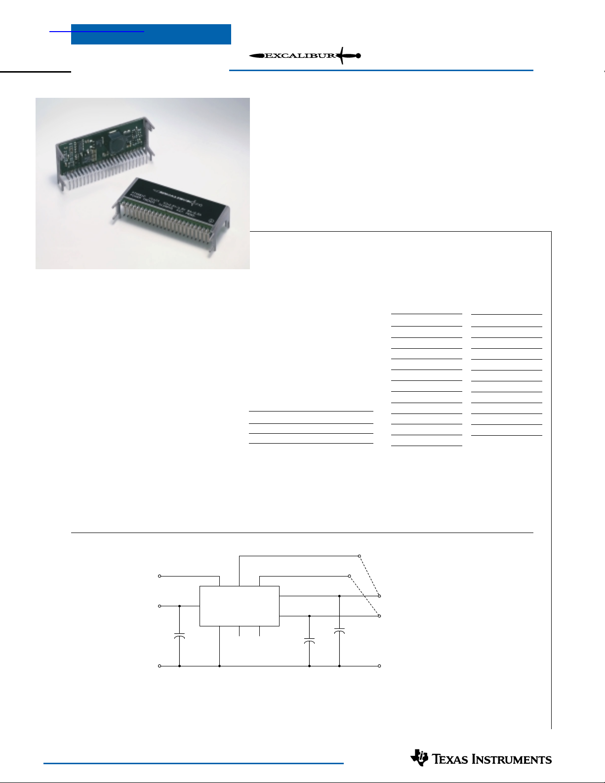
PT6980 Series
10-A 12V-Input Dual Output
Integrated Switching Regulator
Description
The PT6980 Excalibur™ series of
power modules are dual output integrated
switching regulators (ISRs) specifically
designed to power mixed signal ICs.
Operating from a 12-V input bus, the dual
output provides power for both the digital
I/O logic and a DSP core from a single
module. Both output voltages are internally
sequenced during power-up and powerdown to comply with the requirements of
the latest DSP chips. Each output is independently adjustable or can be set to at
least one alternative bus voltage with a
simple pin-strap. The modules are made
available in a space-saving solderable case.
The features include output current limit
and short-circuit protection.
Features
• Dual Outputs
(See Ordering Information)
• Ideal Power Source for DSPs
• 12V Input
• Outputs Adjustable
• Remote Sensing (Vo
& Vo2)
1
• Standby Function
Ordering Information
PT6981o = +2.5/1.8 Volts
PT6982o = +3.3/2.5 Volts
PT6983o = +3.3/1.8 Volts
PT6984o = +3.3/1.2 Volts
PT6985o = +2.5/1.2 Volts
PT Series Suffix
Case/Pin Order Package
Configuration Suffix Code
Vertical N (ELF)
Horizontal A (ELG)
SMD C (ELH)
(Reference the applicable package code drawing
for the dimensions and PC layout)
(PT1234x )
SLTS154
Revised (10/2/2001)
• Soft-Start
• Internal Sequencing
• Short Circuit Protection
• 23-pin Space-Saving Package
• Solderable Copper Case
Pin-Out Information
Pin Function
1Vo1 Sense
2 No Connect
3 STBY
4V
in
5V
in
6V
in
7GND
8GND
9GND
10 GND
11 GND
12 Vo
1
* Vo
and Vo2 can be pin-strapped to another voltage.
1
See application note on output voltage adjustment.
Pin Function
13 Vo
1
14 Vo
1
15 Vo
1
16 Vo1 Adjust *
17 No Connect
18 Vo
2
19 Vo
2
20 Vo
2
21 Vo
2
22 Vo2 Sense
23 Vo2 Adjust *
Standard Application
For technical support and more information, see inside back cover or visit www.ti.com
STBY
V
IN
GND
Vo2 Sense
Vo1 Sense
22
3
4,5,6
C
1
PT6980
7-11
1
18-21
12-15
16
23
+
C
2
+
C
3
GND
Vo
Vo
2
1
C1 = Req’d 560µF electrolytic
C2 = Req’d 330µF electrolytic
C3 = Optional 100µF electrolytic
Page 2
PT6980 Series
10-A 12V-Input Dual Output
Integrated Switching Regulator
General Specifications (Unless otherwise stated, T
Characteristic Symbol Conditions Min Typ Max Units
Short Circuit Current I
Switching Frequency ƒ
Standby (Pin 3) Referenced to GND (pin 7)
Input High Voltage V
Input Low Voltage V
Input Low Current I
Standby Input Current Iin standby pin 3 to GND — 4 6 mA
External Output Capacitance C
Maximum Operating T
Temperature Range
Storage Temperature T
Mechanical Shock Per Mil-STD-883D, Method 2002.3
Mechanical Vibration Per Mil-STD-883D, Method 2007.2
Weight — Vertical/Horizontal — 2 6 — grams
Flammability — Meets UL 94V-O
Notes: (1) The Standby (pin 3) has an internal pull-up to Vin, and if it is left open circuit the module will operate when input power is applied.Refer to the application
Input/Output Capacitors: The PT6980 series requires a 330µF electrolytic capacitor at both the input and output for proper operation (300µF for Oscon® or low ESR
tantalum). In addition, the input capacitance must be rated for a minimum of 1.0Arms ripple current. For transient or dynamic load applications, additional capacitance
may be required. Refer to the application notes for more information.
notes for interface considerations.
(2) The total combined ESR of all output capacitance at 100kHz must be (less than) <50 mΩ.
(3) For operating temperatures below 0°C, Cin and Cout must have stable characteristics. Use either tantalum or Oscon® capacitors.
(4) See Safe Operating Area curves for the specific output voltage combination, or contact the factory for the appropriate derating.
sc
o
IH
IL
IL
2
C
3
a
s
=25°C, Vin =12V)
a
PT6980 Series
Io1 + I o2 combined — 19 — A
Over Vin range 500 550 600 kHz
— — Open
–0.1 — +0.4
— -0.5 – mA
(2)
330
0 — 330
Over Vin Range –40
— –40 — +125 °C
1 msec, ½ Sine, mounted — 500 — G ’s
20-2000 Hz, Soldered in a PC board — 15 — G ’s
— 15,000
(3)
— +85
(1)
V
(2)
µF
(4)
°C
Power-up Sequencing and Vo1/Vo2 Loading
Power-up Sequencing
The PT6980 series of regulators provide two output voltages,
and Vo2. Each of the output voltage combinations
Vo
1
offered by the PT6980 series provides power for both a lowvoltage processor core, and the associated digital support
circuitry. In addition, each output is internally sequenced
during power-up and power-down to comply with the
requirements of most DSP and µP IC’s, and their accompanying chipsets. Figure 1 shows the typical waveforms of the
output voltages, Vo1 and Vo2, from the instance that either
input power is applied or the module is enabled via the
Standby pin. Following a delay of about 25 milli-secs, the
voltages at Vo1 and Vo2 rise together until Vo2 reaches its
set-point. Then Vo1 continues to rise until both output
voltages have reached full voltage.
Figure 1; PT6980 Series Power-up
V1 (1V/Div)
Vo
/Vo2 Loading
1
The output voltages from the PT6980 series regulators are
independently regulated. The voltage at Vo
is produced
1
by a highly efficient switching regulator. The lower output
voltage, Vo2, is derived from Vo1. The regulation method
used for Vo2 also provides control of this output voltage
during power-down. Vo2 will sink current if the voltage at
Vo1 attempts to fall below it.
The load specifications for each model of the PT6980
series gives both a ‘Typical’ (Typ) and ‘Maximum’ (Max)
load current for each output. For operation within the
product’s rating, the load currents at Vo
and Vo2 must
1
comply with the following limits:-
•Io2 must be less than Io2(max).
• The sum-total current from both outputs (Io
+ Io2)
1
must not exceed Io1(max).
In the case that either Vo
or Vo2 are adjusted to some
1
other value than the default output voltage, the absolute
maximum load current for Io2 must be revised to comply
with the following equation.
HORIZ SCALE: 5ms/Div
V2 (1V/Div)
Vstby (10V/Div)
Io2 (max) =
Consult the specification table for each model of the series
Vo
2.5
– Vo
1
Adc
2
for the actual numeric values.
For technical support and more information, see inside back cover or visit www.ti.com
Page 3
PT6981
)
(A)
)
(A)
(typ) ]
(typ) ]
10.5-A 12V-Input Dual Output
Integrated Switching Regulator
PT6981 Performance Specifications (Unless otherwise stated, T
=25°C, Vin =12V, C1 =560µF, C2 =330µF, Io1 =Io1typ, and Io2 =Io2typ)
a
PT6981 (2.5V/1.8V)
Characteristic Symbol Conditions Min Typ Max Units
Output Current Io
Io
Io
Io
Input Voltage Range V
Set Point Voltage Tolerance V
Temperature Variation Reg
Line Regulation Reg
Load Regulation Reg
Total Output Voltage Variation ∆V
1
2
1
2
in
tol Vo
o
temp
line
load
tot Includes set-point, line, load Vo
o
Ta =25°C, natural convection Vo1 (2.5V) 0.1
Ta =60°C, 200LFM airflow Vo1 (2.5V) 0.1
Vo2 (1.8V) 0 2.5
Vo2 (1.8V) 0 2.5
Over Io Range 10.8 — 13.2 VDC
–40° >Ta > +85°C Vo
Over Vin range Vo
Over Io range Vo
–40° >Ta > +85°C Vo
(i)
(i)
— ±12 ±38
1
Vo
— ± 9 ±27
2
— ±0.5 —
1
Vo
— ±0.5 —
2
— ±10 ±15 mV
1
Vo
—±5±7
2
— ±10 ±15
1
Vo
—±5±7
2
— ±44 —
1
— ±28 —
2
(ii)
8
(ii)
(ii)
8
(ii)
10.5
2.5
10.5
2.5
(iii)
A
(iii)
(iii)
A
(iii)
mV
%V
o
mV
mV
Efficiency η —80—%
Vo Ripple (pk-pk) V
Transient Response t
∆V
r
tr
tr
20MHz bandwidth Vo
—35—
1
Vo
—35—
2
1A/µs load step, 50% to 100% Iotyp — 6 0 — µs
Vo over/undershoot Vo
— ±50 —
1
Vo
— ±20 —
2
mV
mV
pp
Notes: (i) Io1(min) current of 0.1A can be divided between both outputs, Vo1 or Vo2. The module will operate at no load with reduced specifications.
(ii) The typical current is that which can be drawn simultaneously from both outputs under the stated operating conditions.
(iii) The sum of Io
and Io2 must be less than Io1max, and Io2 must be less than Io2max.
1
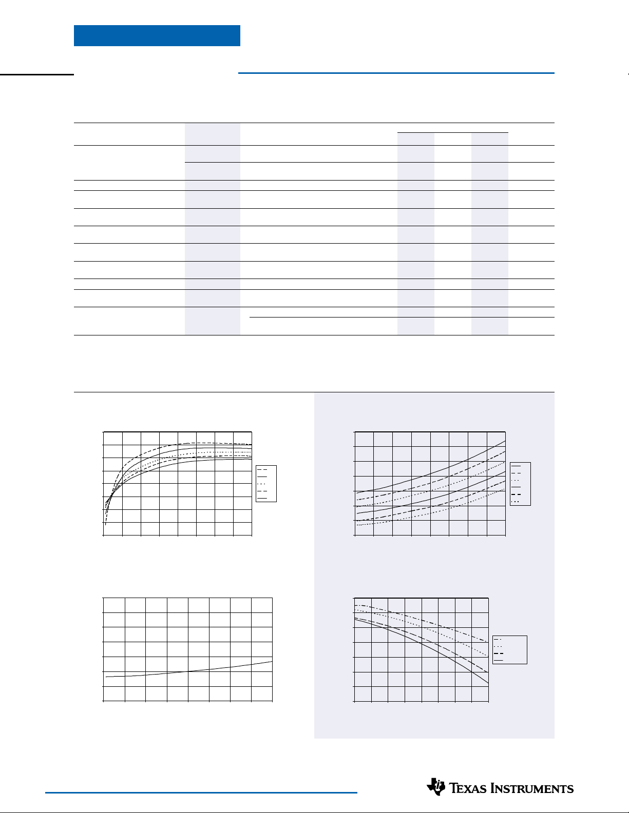
PT6981 Typical Characteristics
Efficiency vs Io1 (See Note A)
90
85
80
75
70
65
Efficiency - %
60
55
50
012345678
Vo1 Output Ripple vs Io1 (See Note A)
70
60
50
40
30
Ripple - mV
20
10
0
012345678
Io1 (A
Io1 (A) [ Io2 fixed at Io
2
Io
Power Dissipation vs Io1 (See Note A)
7
6
2
0.5
1
1.5
2
2.5
5
4
3
Pd - Watts
2
1
0
012345678
Safe Operating Area, Vin =12V (See Note B)
90
80
70
60
50
40
Ambient Temperature (°C)
30
20
012345678
Io1 (A) [ Io2 fixed at Io
Io1 (A
2
Airflow
200LFM
120LFM
60LFM
Nat conv
Io
2
2.5
2
1.5
1
0.5
0.1
Note A: Characteristic data has been developed from actual products tested at 25°C. This data is considered typical data for the Converter.
Note B: SOA curves represent the conditions at which internal components are at or below the manufacturer’s maximum operating temperatures
For technical support and more information, see inside back cover or visit www.ti.com
Page 4
PT6982
)
(A)
)
(A)
(typ) ]
(typ) ]
10.5-A 12V-Input Dual Output
Integrated Switching Regulator
PT6982 Performance Specifications (Unless otherwise stated, T
=25°C, Vin =12V, C1 =560µF, C2 =330µF, Io1 =Io1typ, and Io2 =Io2typ)
a
PT6982 (3.3V/2.5V)
Characteristic Symbol Conditions Min Typ Max Units
Output Current Io
Io
Io
Io
Input Voltage Range V
Set Point Voltage Tolerance V
Temperature Variation Reg
Line Regulation Reg
Load Regulation Reg
Total Output Voltage Variation ∆V
1
2
1
2
in
tol Vo
o
temp
line
load
tot Includes set-point, line, load Vo
o
Ta =25°C, natural convection Vo1 (3.3V) 0.1
Ta =60°C, 200LFM airflow Vo1 (3.3V) 0.1
Vo2 (2.5V) 0 2
Vo2 (2.5V) 0 2
Over Io Range 10.8 — 13.2 VDC
–40° >Ta > +85°C Vo
Over Vin range Vo
Over Io range Vo
–40° >Ta > +85°C Vo
(i)
(i)
— ±16 ±50
1
Vo
— ±12 ±38
2
— ±1.0 —
1
Vo
— ±0.5 —
2
— ±10 ±15
1
Vo
—±5±7
2
— ±10 ±15
1
Vo
— ±10 ±13
2
— ±69 —
1
— ±39 —
2
(ii)
8.5
(ii)
(ii)
8.5
(ii)
10.5
2.25
10.5
2.25
(iii)
A
(iii)
(iii)
A
(iii)
mV
%V
o
mV
mV
mV
Efficiency η —84—%
Ripple (pk-pk) V
V
o
Transient Response t
Notes: (i) Io
(min) current of 0.1A can be divided between both outputs, Vo1 or Vo2. The module will operate at no load with reduced specifications.
1
(ii) The typical current is that which can be drawn simultaneously from both outputs under the stated operating conditions.
(iii) The sum of Io
and Io2 must be less than Io1max, and Io2 must be less than Io2max.
1
∆V
r
tr
tr
20MHz bandwidth Vo
—35—
1
Vo
—35—
2
1A/µs load step, 50% to 100% Iotyp — 6 0 — µs
Vo over/undershoot Vo
— ±50 —
1
Vo
— ±30 —
2
mV
mV
pp
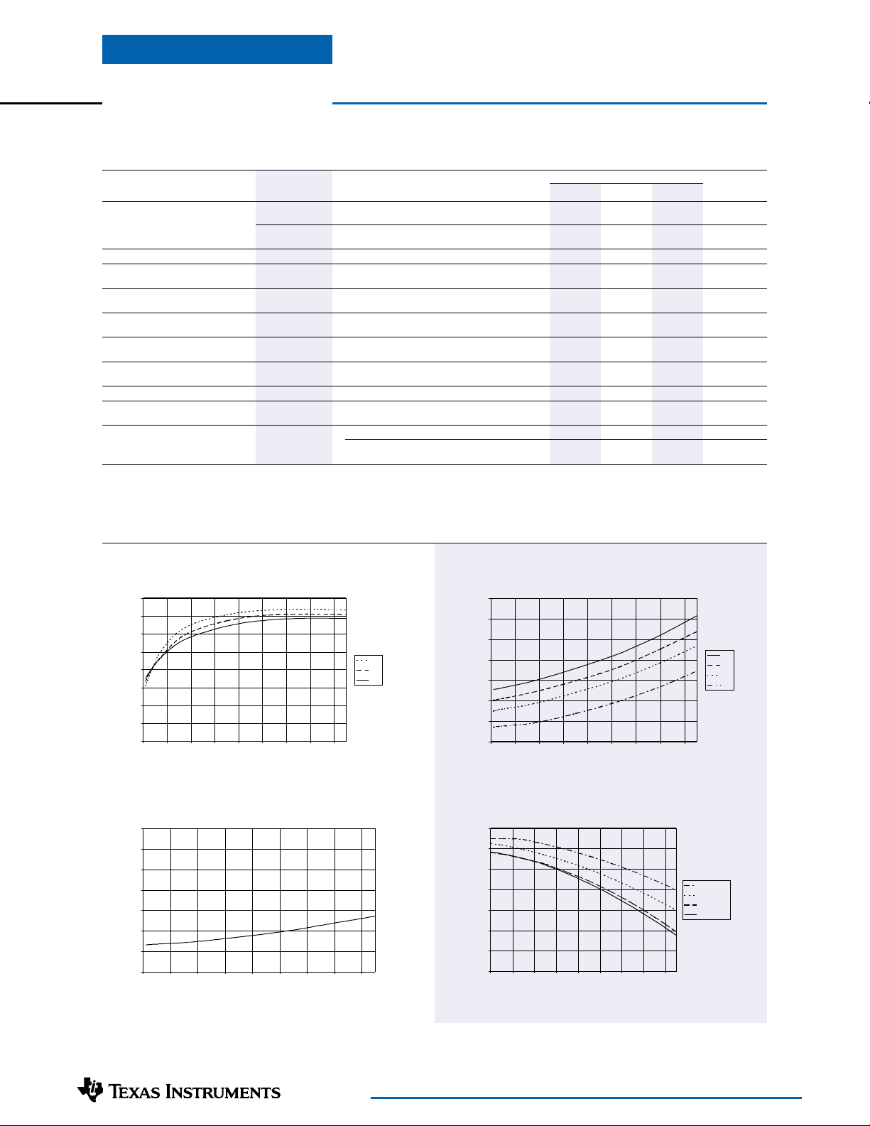
PT6982 Typical Characteristics
Efficiency vs Io1 (See Note A)
90
85
80
75
70
65
Efficiency - %
60
55
50
012345678
Vo1 Output Ripple vs Io1 (See Note A)
70
60
50
40
30
Ripple - mV
20
10
0
012345678
Io1 (A
Io1 (A) [ Io2 fixed at Io
2
Power Dissipation vs Io1 (See Note A)
7
6
Io
2
1
1.5
2
5
4
3
Pd - Watts
2
1
0
012345678
Safe Operating Area, Vin =12V (See Note B)
90
80
70
60
50
40
Ambient Temperature (°C)
30
20
012345678
Io1 (A) [ Io2 fixed at Io
Io1 (A
2
Io
Airflow
200LFM
120LFM
60LFM
Nat conv
2
2
1.5
1
0.1
Note A: Characteristic data has been developed from actual products tested at 25°C. This data is considered typical data for the Converter.
Note B: SOA curves represent the conditions at which internal components are at or below the manufacturer’s maximum operating temperatures
For technical support and more information, see inside back cover or visit www.ti.com
Page 5

PT6983
)
(A)
)
(A)
(typ) ]
(typ) ]
9.5-A 12V-Input Dual Output
Integrated Switching Regulator
PT6983 Performance Specifications (Unless otherwise stated, T
=25°C, Vin =12V, C1 =560µF, C2 =330µF, Io1 =Io1typ, and Io2 =Io2typ)
a
PT6983 (3.3V/1.8V)
Characteristic Symbol Conditions Min Typ Max Units
Output Current Io
Io
Io
Io
Input Voltage Range V
Set Point Voltage Tolerance V
Temperature Variation Reg
Line Regulation Reg
Load Regulation Reg
Total Output Voltage Variation ∆V
1
2
1
2
in
tol Vo
o
temp
line
load
tot Includes set-point, line, load Vo
o
Ta =25°C, natural convection Vo1 (3.3V) 0.1
Ta =60°C, 200LFM airflow Vo1 (3.3V) 0.1
Vo2 (1.8V) 0 2
Vo2 (1.8V) 0 2
Over Io Range 10.8 — 13.2 VDC
–40° >Ta > +85°C Vo
Over Vin range Vo
Over Io range Vo
–40° >Ta > +85°C Vo
(i)
(i)
— ±16 ±50
1
Vo
— ± 9 ±27
2
— ±1.0 —
1
Vo
— ±0.5 —
2
— ±10 ±15 mV
1
Vo
—±5±7
2
— ±10 ±15
1
Vo
—±5±7
2
— ±69 —
1
— ±28 —
2
(ii)
7.5
(ii)
(ii)
7.5
(ii)
(iii)
9.5
2
9.5
2
A
(iii)
(iii)
A
(iii)
mV
%V
o
mV
mV
Efficiency η —81—%
Ripple (pk-pk) V
V
o
Transient Response t
Notes: (i) Io
(min) current of 0.1A can be divided between both outputs, Vo1 or Vo2. The module will operate at no load with reduced specifications.
1
(ii) The typical current is that which can be drawn simultaneously from both outputs under the stated operating conditions.
(iii) The sum of Io
and Io2 must be less than Io1max, and Io2 must be less than Io2max.
1
∆V
r
tr
tr
20MHz bandwidth Vo
—35—
1
Vo
—35—
2
1A/µs load step, 50% to 100% Iotyp — 6 0 — µs
Vo over/undershoot Vo
— ±50 —
1
Vo
— ±20 —
2
mV
mV
pp
PT6983 Typical Characteristics
Efficiency vs Io1 (See Note A)
90
85
80
75
70
65
Efficiency - %
60
55
50
01234567
Vo1 Output Ripple vs Io1 (See Note A)
70
60
50
40
30
Ripple - mV
20
10
0
01234567
Io1 (A
Io1 (A) [ Io2 fixed at Io
2
Power Dissipation vs Io1 (See Note A)
8
7
Io
2
1
1.5
2
6
5
4
Pd - Watts
3
2
1
0
01234567
Safe Operating Area, Vin =12V (See Note B)
90
80
70
60
50
40
Ambient Temperature (°C)
30
20
01234567
Io1 (A) [ Io2 fixed at Io
Io1 (A
2
Io
Airflow
200LFM
120LFM
60LFM
Nat conv
2
2
1.5
1
0.1
Note A: Characteristic data has been developed from actual products tested at 25°C. This data is considered typical data for the Converter.
Note B: SOA curves represent the conditions at which internal components are at or below the manufacturer’s maximum operating temperatures
For technical support and more information, see inside back cover or visit www.ti.com
Page 6

PT6984
)
(A)
(typ) ]
)
(A)
(typ) ]
8.6-A 12V-Input Dual Output
Integrated Switching Regulator
PT6984 Performance Specifications (Unless otherwise stated, T
=25°C, Vin =12V, C1 =560µF, C2 =330µF, Io1 =Io1typ, and Io2 =Io2typ)
a
PT6984 (3.3V/1.2V)
Characteristic Symbol Conditions Min Typ Max Units
Output Current Io
Io
Io
Io
Input Voltage Range V
Set Point Voltage Tolerance V
Temperature Variation Reg
Line Regulation Reg
Load Regulation Reg
Total Output Voltage Variation ∆V
1
2
1
2
in
tol Vo
o
temp
line
load
tot Includes set-point, line, load Vo
o
Ta =25°C, natural convection Vo1 (3.3V) 0.1
Ta =60°C, 200LFM airflow Vo1 (3.3V) 0.1
Vo2 (1.2V) 0 1.6
Vo2 (1.2V) 0 1.6
Over Io Range 10.8 — 13.2 VDC
–40° >Ta > +85°C Vo
Over Vin range Vo
Over Io range Vo
–40° >Ta > +85°C Vo
(i)
(i)
— ±16 ±50
1
Vo
— ± 6 ±18
2
— ±1.0 —
1
Vo
— ±0.5 —
2
— ±10 ±15 mV
1
Vo
—±5±7
2
— ±10 ±15
1
Vo
—±5±7
2
— ±69 —
1
— ±22 —
2
(ii)
7
(ii)
(ii)
7
(ii)
(iii)
8.6
1.6
8.6
1.6
A
(iii)
(iii)
A
(iii)
mV
%V
o
mV
mV
Efficiency η —78—%
Ripple (pk-pk) V
V
o
Transient Response t
Notes: (i) Io
(min) current of 0.1A can be divided between both outputs, Vo1 or Vo2. The module will operate at no load with reduced specifications.
1
(ii) The typical current is that which can be drawn simultaneously from both outputs under the stated operating conditions.
(iii) The sum of Io
and Io2 must be less than Io1max, and Io2 must be less than Io2max.
1
∆V
r
tr
tr
20MHz bandwidth Vo
—35—
1
Vo
—35—
2
1A/µs load step, 50% to 100% Iotyp — 6 0 — µs
Vo over/undershoot Vo
— ±50 —
1
Vo
— ±20 —
2
mV
mV
pp
PT6984 Typical Characteristics
Efficiency vs Io1 (See Note A)
90
85
80
75
70
65
Efficiency - %
60
55
50
01234567
Vo1 Output Ripple vs Io1 (See Note A)
70
60
50
40
30
Ripple - mV
20
10
0
01234567
Io1 (A
Io1 (A) [ Io2 fixed at Io
2
Io
2
0.5
0.75
1
1.25
1.6
Power Dissipation vs Io1 (See Note A)
8
7
6
5
4
Pd - Watts
3
2
1
0
01234567
Safe Operating Area, Vin =12V (See Note B)
90
80
70
60
50
40
Ambient Temperature (°C)
30
20
01234567
Io1 (A) [ Io2 fixed at Io
Io1 (A
2
Io
Airflow
200LFM
120LFM
60LFM
Nat conv
2
1.6
1.25
1.0
0.75
0.5
0.1
Note A: Characteristic data has been developed from actual products tested at 25°C. This data is considered typical data for the Converter.
Note B: SOA curves represent the conditions at which internal components are at or below the manufacturer’s maximum operating temperatures
For technical support and more information, see inside back cover or visit www.ti.com
Page 7

PT6985
)
(A)
(typ) ]
)
(A)
(typ)
)
9-A 12V-Input Dual Output
Integrated Switching Regulator
PT6985 Performance Specifications (Unless otherwise stated, T
=25°C, Vin =12V, C1 =560µF, C2 =330µF, Io1 =Io1typ, and Io2 =Io2typ)
a
PT6985 (2.5V/1.2V)
Characteristic Symbol Conditions Min Typ Max Units
Output Current Io
Io
Io
Io
Input Voltage Range V
Set Point Voltage Tolerance V
Temperature Variation Reg
Line Regulation Reg
Load Regulation Reg
Total Output Voltage Variation ∆V
1
2
1
2
in
tol Vo
o
temp
line
load
tot Includes set-point, line, load Vo
o
Ta =25°C, natural convection Vo1 (2.5V) 0.1
Ta =60°C, 200LFM airflow Vo1 (2.5V) 0.1
Vo2 (1.2V) 0 2
Vo2 (1.2V) 0 2
Over Io Range 10.8 — 13.2 VDC
–40° >Ta > +85°C Vo
Over Vin range Vo
Over Io range Vo
–40° >Ta > +85°C Vo
(i)
(i)
— ±12 ±38
1
Vo
— ± 6 ±18
2
— ±0.5 —
1
Vo
— ±0.5 —
2
— ±10 ±15 mV
1
Vo
—±5±7
2
— ±10 ±15
1
Vo
—±5±7
2
— ±44 —
1
— ±22 —
2
(ii)
7
(ii)
(ii)
7
(ii)
(iii)
9
2.2
9
2.2
A
(iii)
(iii)
A
(iii)
mV
%V
o
mV
mV
Efficiency η —77—%
Ripple (pk-pk) V
V
o
Transient Response t
Notes: (i) Io
(min) current of 0.1A can be divided between both outputs, Vo1 or Vo2. The module will operate at no load with reduced specifications.
1
(ii) The typical current is that which can be drawn simultaneously from both outputs under the stated operating conditions.
(iii) The sum of Io
and Io2 must be less than Io1max, and Io2 must be less than Io2max.
1
∆V
r
tr
tr
20MHz bandwidth Vo
—35—
1
Vo
—35—
2
1A/µs load step, 50% to 100% Iotyp — 6 0 — µs
Vo over/undershoot Vo
— ±50 —
1
Vo
— ±20 —
2
mV
mV
pp
PT6985 Typical Characteristics
Efficiency vs Io1 (See Note A)
90
85
80
75
70
65
Efficiency - %
60
55
50
01234567
Vo1 Output Ripple vs Io1 (See Note A)
30
25
20
15
Ripple - mV
10
5
0
01234567
Io1 (A
Io1 (A) [ Io2 fixed at Io
2
Io
2
Power Dissipation vs Io1 (See Note A)
7
6
5
1
1.5
2
4
3
Pd - Watts
2
1
0
01234567
Safe Operating Area, Vin =12V (See Note B)
90
80
70
60
50
40
Ambient Temperature (°C
30
20
01234567
Io1 (A) [ Io2 fixed at Io
Io1 (A
]
2
Airflow
200LFM
120LFM
60LFM
Nat conv
Io
2
2
1.5
1
0.1
Note A: Characteristic data has been developed from actual products tested at 25°C. This data is considered typical data for the Converter.
Note B: SOA curves represent the conditions at which internal components are at or below the manufacturer’s maximum operating temperatures
For technical support and more information, see inside back cover or visit www.ti.com
Page 8

Application Notes
PT6980 Series
Capacitor Recommendations for the
Dual-Output PT6980 Regulator Series
Input Capacitors:
The recommended input capacitance is determined by 1.0
ampere minimum ripple current rating and 330µF minimum
capacitance . Ripple current and <100mΩ equivalent se-
ries resistance (ESR) values are the major considerations,
along with temperature, when designing with different
types of capacitors. Tantalum capacitors have a recommended
minimum voltage rating of 2 × the maximum DC voltage +
AC ripple. This is necessary to insure reliability for input
voltage bus applications
Output Capacitors: C
(Required), C3(Optional)
2
The ESR of the required capacitor (C2) must not be greater
than 50mΩ. Electrolytic capacitors have poor ripple per-
formance at frequencies greater than 400kHz but excellent
low frequency transient response. Above the ripple frequency, ceramic capacitors are necessary to improve the
transient response and reduce any high frequency noise
components apparent during higher current excursions.
Preferred low ESR type capacitor part numbers are identified
in Table 1. The optional 100µF capacitor (C3) for V2out can
have an ESR of up to 200mΩ for optimum performance
and ripple reduction. (Note: Vendor part numbers for the
optional capacitor, C3, are not identified in the table. Use the
same series selected for C2)
Tantalum Capacitors
Tantalum type capacitors may be used at the output, but
only the AVX TPS series, Sprague 593D/594/595 series,
or Kemet T495/T510 series. The AVX TPS series, Kemet
or Sprague series tantalums are recommended over many
other types due to their higher rated surge, power dissipation,
and ripple current capability. As a caution, the TAJ series
by AVX is not recommended. This series has considerably
higher ESR, reduced power dissipation and lower ripple
current capability. The TAJ Series is also less reliable than
the AVX TPS series when determining power dissipation
capability. Tantalum or Oscon® types are recommended
for applications where ambient temperatures fall below 0°C.
Capacitor Table
Table 1 identifies the characteristics of capacitors from a
number of vendors with acceptable ESR and ripple current
(rms) ratings. The number of capacitors required at both the
input and output buses is identified for each capacitor type.
This is not an extensive capacitor list. Capacitors from other
vendors are available with comparable specifications. Those listed
are for guidance. The RMS ripple current rating and ESR
(Equivalent Series Resistance at 100kHz) are critical parameters
necessary to insure both optimum regulator performance and
long capacitor life.
Table 1: Input/Output Capacitors
roticapaC
/rodneV
tnenopmoC
seireS
cinosanaP
CF
detinU
noc-imehC
/ZXL/VXL
SF/XF
nocihciN
/LP
MP
cinosanaP
CF
gtMecafruS
/SSnocsOVS
XVA
mulatnaT
SPT
temeK
015T
594T
eugarpS
D495
N/R –Not recommended. The voltage rating does not meet the minimin operating limits.
gnikroW
egatloV)Fµ(eulaV
V53
V53
V05
V53
V05
V01
V02
V53
V52
V53
V53
V53
V53
V01
V01
V01
V01
V01
V01
V01Fµ033540.0 Ω Am0532
scitsiretcarahCroticapaCytitnauQ
tnelaviuqE)RSE(
ecnatsiseRseireS
Fµ086
Fµ065
Fµ086
Fµ086
Fµ086
Fµ093
Fµ051
065Fµ
028Fµ
065Fµ
033Fµ
0001Fµ
074Fµ
033Fµ
Fµ033
Fµ033
Fµ022
Fµ033
Fµ022
340.0 Ω
830.0 Ω
840.0 Ω
830.0 Ω
840.0 Ω
030.0 Ω
420.0 Ω
840.0 Ω
940.0 Ω
8400.0 Ω
560.0 ÷2Ω
830.0 Ω
340.0 Ω
520.0 Ω
520.0 Ω
060.0 ÷2Ω
060.0 ÷2Ω
330.0 Ω
70.0 Ω÷ 530.0=2 Ω
elppiRmumixaMC°58
)smrI(tnerruC
Am0961
Am5561
Am5381
Am0661
Am0481
Am0803
Am0023
Am0631
Am0431
Am0631
Am5021>
Am0002
Am0961
Am0053>
Am0083>
Am0052>
Am0003>
Am0041
Am0002>
lacisyhP
tupnI
)mm(eziS
51x61
02x5.21
02x61
02x5.21
02x61
5.01x8
5.01x8
51x61
51x61
51x61
5.61x5.21
5.61x81
5.61x61
5.01x0.01
3.01x3.01
xL3.7
xW3.4
W7.5xL3.7
H0.4x
xL3.7
xW0.6
H1.4
tuptuO
suB
suB
1
1
1
1
1
1
1
1
1
1
R/N
1
4
2
1
1
1
1
1
1
212
1
1
R/N
1
R/N
1
R/N
2
R/N
2
R/N
1
R/N
2
R/N1 T2R0100X733D495
rebmuNrodneV
S186V1CFUEE
S165V1CFUEE
186H1CFUEE
LL02X211M186BV53ZXL
LL02X61M186BV05ZXL
M093XF01
M051XF02
6HHM165V1LPU
6HHM128E1LPU
6HHM165V1MPU
QL133V1CFVEE
N1201V1CFVEE
N174V1CFVEE
M033SS01
M033VS01
)VS(tnuoMecafruS
0600R010M733VSPT
0600R010M722VSPT
SA010M733X015T
SA010M722X594T
For technical support and more information, see inside back cover or visit www.ti.com
Page 9

Application Notes
PT6980 Series
Adjusting the Output Voltage of the PT6980
Dual-Output Voltage Regulators
Each output voltage from the PT6980 series of integrated
switching regulators (ISRs) can be independently adjusted
higher or lower than the factory trimmed pre-set voltage.
The voltages, Vo
down using a single external resistor 1. Table 1 gives the
adjustment range for both Vo
the series as V
always be lower than Vo1 2.
Vo
Adjust Up: To increase the output, add a resistor R
1
between pin 16 (V1 Adjust) and pins 7-11 (GND) 1.
Vo
Adjust Down: Add a resistor (R3), between pin 16
1
(Vo1 Adjust) and pin 1 (Vo1 Sense) 1.
Vo
Adjust Up: Add a resistor R2 between pin 23
2
(Vo2 Adjust) and pins 7-11 (GND) 1.
Vo
Adjust Down: Add a resistor (R1) between pin 23
2
(Vo2 Adjust) and pin 22 (Vo2 Sense) 1.
Refer to Figure 1 and Table 2 for both the placement and value of
the required resistor.
Notes:
1. Use only a single 1% resistor in either the (R
location to adjust Vo1, and in the (R1) or R2 location to
adjust Vo
possible.
2. Vo2 must always be at least 0.2V lower than Vo1.
and Vo2 may be adjusted either up or
1
and Vo2 for each model in
(min) and Va(max). Note that Vo2 must
a
. Place the resistor as close to the ISR as
2
1
) or R
3
4
4
3. Both the Vo1 and Vo2 may be adjusted down to an
alternative bus voltage by making, (R
) or (R1)
3
respectively, a zero ohm link. Refer to the Table 1
footnotes for guidance.
4. Never connect capacitors to either the Vo
Adjust pins. Any capacitance added to these control
Vo
2
Adjust or
1
pins will affect the stability of the respective regulated
output.
5. Adjusting either voltage (Vo1 or Vo2) may increase the
power dissipation in the regulator, and change the
maximum current available at either output. Consult
the note on p.2 of the data sheet regarding Vo
/Vo
1
2
loading.
The adjust up and adjust down resistor values can also be
calculated using the following formulas. Be sure to select
the correct formula parameter from Table 1 for the output
and model being adjusted.
(R1) or (R3) =
(R2) or (R4) =
V
V
10 · V
– V
a
o
a
– V
o
a
r
– R
– R
kΩ
s
kΩ
s
– Vr )
10 (V
Where: Vo= Original output voltage, (Vo1 or Vo2)
Va= Adjusted output voltage
Vr= The reference voltage from Table 1
Rs= The series resistance from Table 1
Figure 1
Vo2 (sns)
4,5,6
V
IN
C
Vin
+
1
GND Vo2 (adj)
STBY
3
PT6980
237 - 11
Vo
Vo
Vo1 (adj)
16
Adj Down
18 - 21
2
12 - 15
1
(R3) (R1)
R4
R2
+
C
2
C
3
1
22
Vo1 (sns)
Adjust Up
COM COM
Adjust Vo
For technical support and more information, see inside back cover or visit www.ti.com
1
Adjust Vo
2
Vo
2
Vo
1
L
L
O
+
O
A
A
D
D
Page 10

Application Notes
PT6980 Series
Table 1
ADJUSTMENT RANGE AND FORMULA PARAMETERS
Vo1 Bus Vo2 Bus
Series Pt # PT6981/85 PT6982/83/84 PT6984/85 PT6981/83 PT6936
Adj. Resistor (R3)/R4 (R3)/R4 (R1)/R2 (R1)/R2 (R1)/R2
Vo(nom) 2.5V 3.3V 1.2V 1.8V 2.5V
Va(min) 1.8V
Va(max) 3.6V 3.6V 1.5V
Vr 1.27V 1.27V 0.6125V 1.0V 1.0V
ΩΩ
Rs (k
Ω) 7.5 15.4 20.0 16.9 11.5
ΩΩ
*
2.5V
*
1.0V
(2)
†
#
†
1.5V
2.4V 3.0
1.8V
†
Ref. Note 3: * (R3) = Zero-ohm link
†(R1) = Zero-ohm link
#
(R2) = Zero-ohm link
Table 2
ADJUSTMENT RESISTOR VALUES
Vo1 Bus
Series Pt # PT6981/85 PT6982/83/84
Adj. Resistor (R3)/R4 (R3)/R4
Vo(nom) 2.5V 3.3V
Va(req’d)
1.8 (0.0)
1.85 (1.4)kΩ
1.9 (3.0)kΩ
1.95 (4.9)kΩ
2.0 (7.1)kΩ
2.05 (9.8)kΩ
2.1 (13.3)kΩ
2.2 (23.5)kΩ
2.3 (44.0)kΩ
2.4 (106.0)kΩ
2.5 (0.0)kΩ
2.6 120.0kΩ (3.6)kΩ
2.7 56.0kΩ (8.4)kΩ
2.8 34.8kΩ (15.2)kΩ
2.9 24.3kΩ (25.4)kΩ
3.0 17.9kΩ (42.3)kΩ
3.1 13.7kΩ (76.1)kΩ
3.2 10.6kΩ (178.0)kΩ
3.3 8.4kΩ
3.4 6.6kΩ 112.0k
3.5 5.2kΩ 48.1k
3.6 4.1kΩ 26.9k
R1/R3 = (Blue), R2/R4 = Black
Vo2 Bus
Series Pt # PT6984/85 PT6981/83 PT6982
Adj. Resistor (R1)/R2 (R1)/R2 (R1)/R2
Vo(nom) 1.2V 1.8V 2.5V
Va(req’d)
1.0 (0.0)kΩ
1.05 (9.2)kΩ
1.1 (28.8)kΩ
1.15 (87.5)kΩ
1.2
1.25 101.5kΩ
1.3 41.2kΩ
1.35 20.8kΩ
1.4 10.6kΩ
1.45 4.5kΩ
1.5 0.0kΩ (0.0)kΩ
1.55 (5.1)kΩ
1.6 (13.1)kΩ
1.65 (26.4)kΩ
1.7 (53.1)kΩ
1.75 (133.0)kΩ
1.8 (0.0)kΩ
1.85 183.0kΩ (1.6)kΩ
1.9 83.1kΩ (3.5)kΩ
1.95 49.8kΩ (5.8)kΩ
2.0 33.1kΩ (8.5)kΩ
2.05 23.1kΩ (11.8)kΩ
2.1 16.4kΩ (16.0)kΩ
2.2 8.1kΩ (28.5)kΩ
2.3 3.1kΩ (53.5)kΩ
2.4 0.0kΩ (129.0)kΩ
2.5
2.6 88.5kΩ
2.7 38.5kΩ
2.8 21.8kΩ
2.9 13.5kΩ
3.0 8.5kΩ
For technical support and more information, see inside back cover or visit www.ti.com
Page 11

Application Notes
PT6980 Series
Using the Standby Function on the PT6980
Series of Dual-Output Voltage Regulators
Both output voltages of the 23-pin PT6980 dual-output
converter may be disabled using the regulator’s ‘Standby’
function. This function may be used in applications that
require power-up/shutdown sequencing, or wherever there
is a requirement to control the output voltage On/Off status
with external circuitry.
The standby function is provided by the STBY* control
(pin 3). If pin 3 is left open-circuit the regulator operates
normally, and provides a regulated output at both Vo
12–15) and Vo2 (pins 18–21) whenever a valid supply voltage is applied to Vin (pins 4, 5, & 6) with respect to GND
1
(pins 7-11). If a low voltage
is then applied to pin-3 both
regulator outputs will be simultaneously disabled and the
input current drawn by the ISR will drop to a typical value
of 4mA. The standby control may also be used to hold-off
both regulator outputs during the period that input power is
applied.
The standby pin is ideally controlled using an open-collector
(or open-drain) discrete transistor (See Figure 1). The
open-circuit voltage is the input voltage +V
. Table 1 gives
in
the circuit parameters for this control input.
Table 1 Standby Control Parameters
Parameter Min TYP Max
Enable (VIH) — — Open circuit
Disable (VIL) –0.1V — 0.4V
V
(open circuit) — +Vin
STBY
I
STBY(IIL
) — — –0.5mA
1, 2
2
(pins
1
1
—
Figure 1
1
22
V1(sns)
V
in
Inhibit
V2(sns)
4, 5, 6
V
PT6984
IN
GND V2(adj)
STBY
Q1
BSS138
3
+
C
1
18–21
Vo
2
12–15
Vo
1
(adj)
V
1
237–11
16
+
C
2
Vo
Vo
+
C
3
COMCOM
Turn-On Time: Turning Q1 in Figure 1 off removes the low-
voltage signal at pin 3 and enables the PT6980 series
regulator. Following a delay of about 25ms, Vo
and Vo
1
rise together until the lower voltage, Vo2, reaches its set
output. Vo
continues to rise until both outputs reach full
1
regulation voltage. The total power-up time is less than
40ms, and is relatively independent of load, temperature,
and output capacitance. Figure 2 shows waveforms of the
output voltages, Vo
The turn-off of Q
and Vo2, for a PT6984 (3.3V/1.2V).
1
corresponds to the rise in V
1
STBY
. The
waveforms were measured with a 12V input voltage, and
with resistive loads of 5A and 1.25A at the Vo
and Vo
1
2
outputs respectively.
Figure 2
2
1
2
Notes:
1. The standby control input is Not compatible with TTL or
other devices that incorporate a totem-pole output drive. Use
only a true open-collector device, preferably a discrete bipolar
transistor (or MOSFET). To ensure the regulator output is
disabled, the control pin must be pulled to less than 0.4Vdc
with a low-level 0.5mA sink to ground.
2 The standby control input
requires no external pull-up resistor.
The open-circuit voltage of the STBY* pin is the input
voltage +V
.
in
3. When the regulator output is disabled the current drawn from
the input source is typically reduced to 4mA.
V1 (1V/Div)
V2 (1V/Div)
Vstby (10V/Div)
HORIZ SCALE: 5ms/Div
For technical support and more information, see inside back cover or visit www.ti.com
Page 12

PACKAGE OPTION ADDENDUM
www.ti.com
13-Oct-2005
PACKAGING INFORMATION
Orderable Device Status
PT6981C ACTIVE SIP MOD
(1)
Package
Type
Package
Drawing
Pins Package
Qty
Eco Plan
ELH 23 10 TBD Call TI Level-3-215C-168HRS
ULE
PT6982C ACTIVE SIP MOD
ELH 23 10 TBD Call TI Level-3-215C-168HRS
ULE
PT6982N ACTIVE SIP MOD
ELF 23 10 TBD Call TI Level-1-215C-UNLIM
ULE
PT6983A ACTIVE SIP MOD
ELG 23 10 TBD Call TI Level-1-215C-UNLIM
ULE
PT6983C ACTIVE SIP MOD
ELH 23 10 TBD Call TI Level-3-215C-168HRS
ULE
PT6983N ACTIVE SIP MOD
ELF 23 10 TBD Call TI Level-1-215C-UNLIM
ULE
PT6984C ACTIVE SIP MOD
ELH 23 10 TBD Call TI Level-3-215C-168HRS
ULE
PT6984N ACTIVE SIP MOD
ELF 23 10 TBD Call TI Level-1-215C-UNLIM
ULE
(1)
The marketing status values are defined as follows:
ACTIVE: Product device recommended for new designs.
LIFEBUY: TI has announced that the device will be discontinued, and a lifetime-buy period is in effect.
NRND: Not recommended for new designs. Device is in production to support existing customers, but TI does not recommend using this part in
a new design.
PREVIEW: Device has been announced but is not in production. Samples may or may not be available.
OBSOLETE: TI has discontinued the production of the device.
(2)
Lead/Ball Finish MSL Peak Temp
(3)
(2)
Eco Plan - The planned eco-friendly classification: Pb-Free (RoHS) or Green (RoHS & no Sb/Br) - please check
http://www.ti.com/productcontent for the latest availability information and additional product content details.
TBD: The Pb-Free/Green conversion plan has not been defined.
Pb-Free (RoHS): TI's terms "Lead-Free" or "Pb-Free" mean semiconductor products that are compatible with the current RoHS requirements
for all 6 substances, including the requirement that lead not exceed 0.1% by weight in homogeneous materials. Where designed to be soldered
at high temperatures, TI Pb-Free products are suitable for use in specified lead-free processes.
Green (RoHS & no Sb/Br): TI defines "Green" to mean Pb-Free (RoHS compatible), and free of Bromine (Br) and Antimony (Sb) based flame
retardants (Br or Sb do not exceed 0.1% by weight in homogeneous material)
(3)
MSL, Peak Temp. -- The Moisture Sensitivity Level rating according to the JEDEC industry standard classifications, and peak solder
temperature.
Important Information and Disclaimer:The information provided on this page represents TI's knowledge and belief as of the date that it is
provided. TI bases its knowledge and belief on information provided by third parties, and makes no representation or warranty as to the
accuracy of such information. Efforts are underway to better integrate information from third parties. TI has taken and continues to take
reasonable steps to provide representative and accurate information but may not have conducted destructive testing or chemical analysis on
incoming materials and chemicals. TI and TI suppliers consider certain information to be proprietary, and thus CAS numbers and other limited
information may not be available for release.
In no event shall TI's liability arising out of such information exceed the total purchase price of the TI part(s) at issue in this document sold by TI
to Customer on an annual basis.
Addendum-Page 1
Page 13

IMPORTANT NOTICE
Texas Instruments Incorporated and its subsidiaries (TI) reserve the right to make corrections, modifications,
enhancements, improvements, and other changes to its products and services at any time and to discontinue
any product or service without notice. Customers should obtain the latest relevant information before placing
orders and should verify that such information is current and complete. All products are sold subject to TI’s terms
and conditions of sale supplied at the time of order acknowledgment.
TI warrants performance of its hardware products to the specifications applicable at the time of sale in
accordance with TI’s standard warranty. Testing and other quality control techniques are used to the extent TI
deems necessary to support this warranty . Except where mandated by government requirements, testing of all
parameters of each product is not necessarily performed.
TI assumes no liability for applications assistance or customer product design. Customers are responsible for
their products and applications using TI components. To minimize the risks associated with customer products
and applications, customers should provide adequate design and operating safeguards.
TI does not warrant or represent that any license, either express or implied, is granted under any TI patent right,
copyright, mask work right, or other TI intellectual property right relating to any combination, machine, or process
in which TI products or services are used. Information published by TI regarding third-party products or services
does not constitute a license from TI to use such products or services or a warranty or endorsement thereof.
Use of such information may require a license from a third party under the patents or other intellectual property
of the third party, or a license from TI under the patents or other intellectual property of TI.
Reproduction of information in TI data books or data sheets is permissible only if reproduction is without
alteration and is accompanied by all associated warranties, conditions, limitations, and notices. Reproduction
of this information with alteration is an unfair and deceptive business practice. TI is not responsible or liable for
such altered documentation.
Resale of TI products or services with statements different from or beyond the parameters stated by TI for that
product or service voids all express and any implied warranties for the associated TI product or service and
is an unfair and deceptive business practice. TI is not responsible or liable for any such statements.
Following are URLs where you can obtain information on other Texas Instruments products and application
solutions:
Products Applications
Amplifiers amplifier.ti.com Audio www.ti.com/audio
Data Converters dataconverter.ti.com Automotive www.ti.com/automotive
DSP dsp.ti.com Broadband www.ti.com/broadband
Interface interface.ti.com Digital Control www.ti.com/digitalcontrol
Logic logic.ti.com Military www.ti.com/military
Power Mgmt power.ti.com Optical Networking www.ti.com/opticalnetwork
Microcontrollers microcontroller.ti.com Security www.ti.com/security
Telephony www.ti.com/telephony
Video & Imaging www.ti.com/video
Wireless www.ti.com/wireless
Mailing Address: Texas Instruments
Post Office Box 655303 Dallas, Texas 75265
Copyright 2005, Texas Instruments Incorporated
 Loading...